

Page 1
ESD Protection Diode
Dual Line Automotive Bus Protector
NUP2125, SZNUP2125
The SZ/NUP2125 has been designed to protect both CAN and LIN
transceivers from ESD and other harmful transient voltage events.
This device provides bidirectional protection for each data line with a
single compact SC−70 (SOT−323) package, giving the system
designer a low cost option for improving system reliability and
meeting stringent EMI requirements.
Features
• 200 W Peak Power Dissipation per Line (8/20 ms Waveform)
• Diode Capacitance Matching
• Low Reverse Leakage Current (< 100 nA)
• IEC Compatibility: − IEC 61000−4−2 (ESD): Level 4
− IEC 61000−4−4 (EFT): 50 A – 5/50 ns
− IEC 61000−4−5 (Lighting) 3.0 A (8/20 ms)
• ISO 7637−1, Nonrepetitive EMI Surge Pulse 2, 8.0 A (1/50 ms)
• ISO 7637−3, Repetitive Electrical Fast Transient (EFT)
EMI Surge Pulses, 50 A (5/50 ns)
• Flammability Rating UL 94 V−0
• SZ Prefix for Automotive and Other Applications Requiring Unique
Site and Control Change Requirements; AEC−Q101 Qualified and
PPAP Capable
• These are Pb−Free Devices
Applications
• Automotive Networks
♦ CAN / CAN−FD
♦ Low and High−Speed CAN
♦ Fault Tolerant CAN
♦ LIN
www.onsemi.com
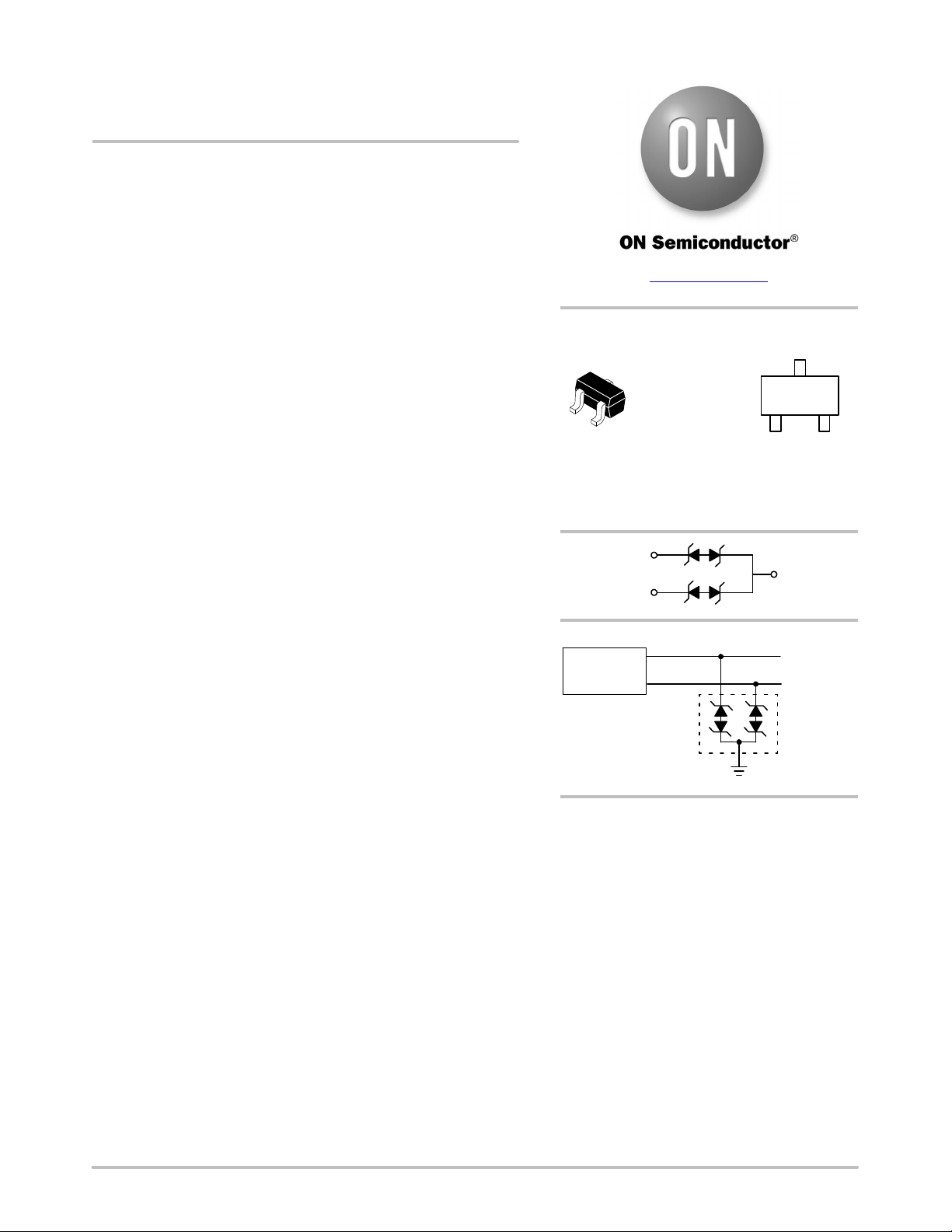
MARKING
DIAGRAM
SC−70
CASE 419
1
25 = Specific Device Code
M = Date Code
G = Pb−Free Package
(Note: Microdot may be in either location)
PIN 1
PIN 2
CAN_H / Single Wire LIN
CAN
Transceiver
CAN_L
CAN Bus
25MG
G
PIN 3
NUP2125
© Semiconductor Components Industries, LLC, 2015
December, 2020 − Rev. 7
ORDERING INFORMATION
See detailed ordering and shipping information on page 2 of
this data sheet.
1 Publication Order Number:
NUP2125/D
Page 2

NUP2125, SZNUP2125
MAXIMUM RATINGS (T
Symbol
PPK
ESD Human Body Model (HBM)
Peak Power Dissipation, 8/20 ms Double Exponential Waveform (Note 1)
T
Operating Junction Temperature Range −55 to 150 °C
J
T
Storage Temperature Range −55 to 150 °C
J
T
Lead Solder Temperature (10 s) 260 °C
L
Machine Model (MM)
IEC 61000−4−2 Contact
IEC 61000−4−2 Air
ISO 10605 150 pF / 2 kW Contact
ISO 10605 330 pF / 2 kW Contact
= 25°C, unless otherwise specified)
J
Rating Value Unit
200 W
±8.0
±1.6
±30
±30
±30
±30
kV
kV
kV
kV
kV
kV
Stresses exceeding those listed in the Maximum Ratings table may damage the device. If any of these limits are exceeded, device functionality
should not be assumed, damage may occur and reliability may be affected.
1. Non−repetitive current pulse per Figure 1.
ELECTRICAL CHARACTERISTICS (T
Symbol
V
RWM
V
BR
I
R
V
C
V
C
I
PP
C
J
Reverse Working Voltage (Note 2) 24 − − V
Breakdown Voltage IT = 1 mA (Note 3) 27 28.5 32 V
Reverse Leakage Current V
Clamping Voltage
Clamping Voltage
Maximum Peak Pulse Current
Capacitance
Parameter Test Conditions Min Typ Max Unit
= 25°C, unless otherwise specified)
J
= 24 V − 15 100 nA
RWM
IPP = 1 A (8/20 ms Waveform)
− 33.4 36.6 V
(Note 4)
IPP = 3 A (8/20 ms Waveform)
− 44 50 V
(Note 4)
8/20 ms Waveform (Note 4)
− − 3.0 A
VR = 0 V, f = 1 MHz (Line to GND) − 7.0 10 pF
VR = 5 V, f = 1 MHz (Line to GND) − 4.5 6.0 pF
DC
VR = 5 V, f = 1 MHz (Line to GND),
T
= +150°C
A
Diode Capacitance Matching VR = 0 V, 5 MHz (Note 5) − 0.26 2 %
− 5.0 − pF
Product parametric performance is indicated in the Electrical Characteristics for the listed test conditions, unless otherwise noted. Product
performance may not be indicated by the Electrical Characteristics if operated under different conditions.
2. Surge protection devices are normally selected according to the working peak reverse voltage (V
than the DC or continuous peak operating voltage level.
is measured at pulse test current IT.
3. V
BR
4. Pulse waveform per Figure 1.
5. DC is the percentage difference between C
table.
of lines 1 and 2 measured according to the test conditions given in the electrical characteristics
J
), which should be equal or greater
RWM
ORDERING INFORMATION
Device Package Shipping
NUP2125WTT1G
SZNUP2125WTT1G*
NUP2125WTT3G
SZNUP2125WTT3G*
SC−70
(Pb−Free)
3000 / Tape & Reel
10000 / Tape & Reel
†For information on tape and reel specifications, including part orientation and tape sizes, please refer to our Tape and Reel Packaging
Specifications Brochure, BRD8011/D.
*SZ Prefix for Automotive and Other Applications Requiring Unique Site and Control Change Requirements; AEC−Q101 Qualified and PPAP
Capable.
†
www.onsemi.com
2
Page 3

NUP2125, SZNUP2125
TYPICAL PERFORMANCE CURVES
(TJ = 25°C unless otherwise noted)
110
100
90
80
70
60
50
40
30
20
% OF PEAK PULSE CURRENT
10
0
0 5 15 25
c−t
td = IPP/2
10 20
t, TIME (ms)
Figure 1. Pulse Waveform, 8 × 20 ms
9
8
125°C
7
6
5
4
C, CAPACITANCE (pF)
3
2
05
25°C
10 15 20 25
V
, REVERSE VOLTAGE (V)
R
Figure 3. Typical Junction Capacitance vs
Reverse Voltage
WAVEFORM
PARAMETERS
= 8 ms
t
r
t
= 20 ms
d
3.5
3.0
2.5
2.0
1.5
1.0
, PEAK PULSE CURRENT (A)
PP
I
0.5
30
0.0
30 35 45 50
Figure 2. Clamping Voltage vs Peak Pulse Current
50
45
40
35
30
25
, (mA)
T
I
20
15
10
5
0
20 22 24 26 28 30 32 34
Figure 4. VBR versus IT Characteristics
40
, CLAMPING VOLTAGE (V)
V
C
25°C
TA = −55°C
V
, VOLTAGE (V)
BR
65°C
125°C
25
−55°C
20
15
10
5
, REVERSE BIAS VOLTAGE (V)
R
V
0
012345
+25°C
TA = +150°C
I
, LEAKAGE CURRENT (nA)
L
Figure 5. IR versus Temperature Characteristics
www.onsemi.com
120
100
80
60
40
20
PERCENT DERATING (%)
0
−60 −30 0 30 60 90 120 150 180
TEMPERATURE (°C)
Figure 6. Temperature Power Dissipation Derating
3
Page 4

NUP2125, SZNUP2125
Surge Protection Diode Circuit
Surge protection diodes provide protection to a
transceiver by clamping a surge voltage to a safe level. Surge
protection diodes have high impedance below and low
impedance above their breakdown voltage. A surge
protection Zener diode has its junction optimized to absorb
the high peak energy of a transient event, while a standard
Zener diode is designed and specified to clamp a
steady state voltage.
Figure 7 provides an example of a dual bidirectional surge
protection diode array that can be used for protection with
the high−speed CAN network. The bidirectional array is
created from four identical Zener TVS diodes. The
clamping voltage of the composite device is equal to the
breakdown voltage of the diode that is reversed biased, plus
the diode drop of the second diode that is forwarded biased.
CAN_H
CAN
Transceiver
Figure 7. High−Speed and Fault Tolerant CAN Surge
CAN_L
Protection Circuit
CAN Bus
NUP2125
www.onsemi.com
4
Page 5

0.05 (0.002)
D
e1
3
H
E
12
e
A1
NUP2125, SZNUP2125
PACKAGE DIMENSIONS
SC−70 (SOT−323)
CASE 419−04
ISSUE N
NOTES:
1. DIMENSIONING AND TOLERANCING PER ANSI Y14.5M, 1982.
2. CONTROLLING DIMENSION: INCH.
DIMAMIN NOM MAX MIN
E
b
A
A2
A1 0.00 0.05 0.10 0.000
A2 0.70 REF
b 0.30 0.35 0.40 0.012
c 0.10 0.18 0.25 0.004
D 1.80 2.10 2.20 0.071
E 1.15 1.24 1.35 0.045
e 1.20 1.30 1.40 0.047
e1
L
H
E
STYLE 11:
c
PIN 1. CATHODE
MILLIMETERS
0.80 0.90 1.00 0.032
0.65 BSC
0.38
0.20 0.56
2.00 2.10 2.40 0.079 0.083 0.095
2. CATHODE
3. CATHODE
L
SOLDERING FOOTPRINT*
0.65
0.65
0.025
0.025
INCHES
NOM MAX
0.035 0.040
0.002 0.004
0.028 REF
0.014 0.016
0.007 0.010
0.083 0.087
0.049 0.053
0.051 0.055
0.026 BSC
0.015
0.008 0.022
1.9
0.075
0.9
0.035
0.7
0.028
SCALE 10:1
mm
ǒ
inches
Ǔ
*For additional information on our Pb−Free strategy and soldering
details, please download the ON Semiconductor Soldering and
Mounting Techniques Reference Manual, SOLDERRM/D.
Honeywell and SDS are registered trademarks of Honeywell International Inc.
DeviceNet is a trademark of Rockwell Automation.
ON Semiconductor and are trademarks of Semiconductor Components Industries, LLC dba ON Semiconductor or its subsidiaries in the United States and/or other countries.
ON Semiconductor owns the rights to a number of patents, trademarks, copyrights, trade secrets, and other intellectual property. A listing of ON Semiconductor’s product/patent
coverage may be accessed at www.onsemi.com/site/pdf/Patent−Marking.pdf
ON Semiconductor makes no warranty, representation or guarantee regarding the suitability of its products for any particular purpose, nor does ON Semiconductor assume any liability
arising out of the application or use of any product or circuit, and specifically disclaims any and all liability, including without limitation special, consequential or incidental damages.
Buyer is responsible for its products and applications using ON Semiconductor products, including compliance with all laws, regulations and safety requirements or standards,
regardless of any support or applications information provided by ON Semiconductor. “Typical” parameters which may be provided in ON Semiconductor data sheets and/or
specifications can and do vary in different applications and actual performance may vary over time. All operating parameters, including “Typicals” must be validated for each customer
application by customer’s technical experts. ON Semiconductor does not convey any license under its patent rights nor the rights of others. ON Semiconductor products are not
designed, intended, or authorized for use as a critical component in life support systems or any FDA Class 3 medical devices or medical devices with a same or similar classification
in a foreign jurisdiction or any devices intended for implantation in the human body. Should Buyer purchase or use ON Semiconductor products for any such unintended or unauthorized
application, Buyer shall indemnify and hold ON Semiconductor and its officers, employees, subsidiaries, affiliates, and distributors harmless against all claims, costs, damages, and
expenses, and reasonable attorney fees arising out of, directly or indirectly, any claim of personal injury or death associated with such unintended or unauthorized use, even if such
claim alleges that ON Semiconductor was negligent regarding the design or manufacture of the part. ON Semiconductor is an Equal Opportunity/Affirmative Action Employer. This
literature is subject to all applicable copyright laws and is not for resale in any manner.
. ON Semiconductor reserves the right to make changes without further notice to any products herein.
PUBLICATION ORDERING INFORMATION
LITERATURE FULFILLMENT:
Literature Distribution Center for ON Semiconductor
P.O. Box 5163, Denver, Colorado 80217 USA
Phone: 303−675−2175 or 800−344−3860 Toll Free USA/Canada
Fax: 303−675−2176 or 800−344−3867 Toll Free USA/Canada
Email: orderlit@onsemi.com
◊
N. American Technical Support: 800−282−9855 Toll Free
USA/Canada
Europe, Middle East and Africa Technical Support:
Phone: 421 33 790 2910
www.onsemi.com
5
ON Semiconductor Website: www.onsemi.com
Order Literature: http://www.onsemi.com/orderlit
For additional information, please contact your local
Sales Representative
NUP2125/D
 Loading...