

Page 1
NUF4220MN
l
Audio EMI Filter, 4 Line,
with ESD Protection
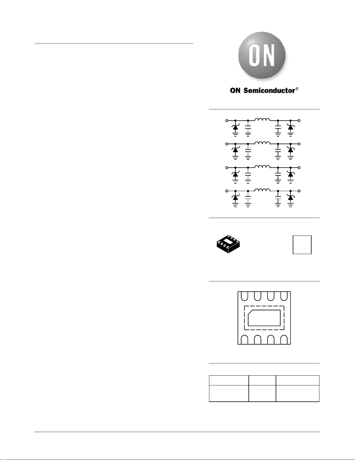
NUF4220MN is a 4 line LC EMI filter array designed for audio
applications. It offers greater than −30 dB attenuation at frequencies
rom 800 MHz to 5.0 GHz, with no line loss. This part is a single chip
f
solution for audio interface applications, 2 speaker lines with a
microphone line. This device also offers ESD protection−clamping
transients from static discharges and ESD protection is provided
across all capacitors.
http://onsemi.com
1
L
C1 C1
8
Features
• Provides EMI Filtering and ESD Protection
• Integration of 20 Discretes
• Compliance with IEC61000−4−2 (Level 4)
18 kV (Contact)
• DFN8, 2x2 mm Package
• Moisture Sensitivity Level 1
• ESD Ratings: Machine Model = C
Human Body Model = 3B
• Excellent Line Efficiency with Low Line Resistance < 1.1 max
• This is a Pb−Free Device*
Applications
• Headset
• MP3s
• PDAs
• Digital Cameras
• Portable DVDs
• Handfree Interface
2
C2 C2
3
C3 C3
4
C4 C4
(Top View)
CASE 506AA
1
R2 = Specific Device Code
M = Date Code
G = Pb−Free Package
PLASTIC
L
L
L
DFN8
MARKING
DIAGRAM
1
4
4321
7
6
5
R2 MG
G
*For additional information on our Pb−Free strategy and soldering details, please
download the ON Semiconductor Soldering and Mounting Techniques
Reference Manual, SOLDERRM/D.
© Semiconductor Components Industries, LLC, 2006
October, 2006 − Rev. 0
1 Publication Order Number:
GND
5678
(Bottom View)
ORDERING INFORMATION
Device Package Shipping
NUF4220MNT1G DFN8
(Pb−Free)
†For information on tape and reel specifications,
including part orientation and tape sizes, please
refer to our Tape and Reel Packaging Specification
Brochure, BRD8011/D.
3000 / Tape & Ree
NUF4220MN/D
†
Page 2
NUF4220MN
MAXIMUM RATINGS
Parameter Symbol Value Unit
ESD Discharge IEC61000−4−2 Contact Discharge V
Steady−State Power per Inductor P
Steady−State Power per Package P
Operating Temperature Range T
Storage Temperature Range T
Maximum Lead Temperature for Soldering Purposes (1.8 in from case for 10 s) T
PP
L
T
OP
stg
L
Stresses exceeding Maximum Ratings may damage the device. Maximum Ratings are stress ratings only. Functional operation above the
Recommended Opera t i n g Conditions is not implied. Extended exposure to stresses above the Recommended Operating Conditions may affect
device reliability.
18 kV
90 mW
360 mW
−40 to 85 °C
−55 to 150 °C
260 °C
ELECTRICAL CHARACTERISTICS (T
Parameter
= 25°C unless otherwise noted)
J
Test Conditions Symbol Min Typ Max Unit
Maximum Reverse Working Voltage V
Breakdown Voltage IR = 1.0 mA V
Leakage Current V
= 3.3 V I
RWM
Inductance
Series Resistance R
Capacitance (Note 1, 3) C
Cut−Off Frequency (Note 2) Above this frequency,
appreciable attenuation occurs
1. Measured at 25°C, VR = 0 V, f = 1.0 MHz.
2. 50 source and 50 load termination.
3. Total line capacitance is 2 times the diode capacitance (C
).
d
RWM
BR
R
L
f
3dB
5.0 V
6.0 7.0 8.0 V
0.1
A
4.9 nH
S
d
0.6 0.85 1.1
205 pF
16 MHz
http://onsemi.com
2
Page 3

NUF4220MN
TYPICAL PERFORMANCE CURVES
(TA = 25°C unless otherwise specified)
0
−5.0
−10
−15
−20
−25
S21 (dB)
−30
−35
−40
−45
1.0E+6 10E+6 100E+6 1.0E+9 10E+9
FREQUENCY (Hz)
Figure 1. Typical Insertion Loss
Characteristics
1.2
1.0
0.8
0
−10
−20
−30
−40
S41 (dB)
−50
−60
−70
−80
10E+6
1.2
1.0
0.8
100E+6 1.0E+9 10E+9
FREQUENCY (MHz)
Figure 2. Typical Analog Crosstalk
0.6
0.4
0.2
NORMALIZED CAPACITANCE
0
0 1.0 2.0 3.0 4.0 5.0
REVERSE BIAS VOLTAGE (V)
Figure 3. Typical Line Capacitance vs.
Reverse Bias Voltage (Normalized to
Capacitance @ 0 V)
0.6
0.4
RESISTANCE ()
0.2
0
−40 −15 10 35 60 85
TEMPERATURE (°C)
Figure 4. Typical Resistance Over Temperature
http://onsemi.com
3
Page 4

MECHANICAL CASE OUTLINE
PACKAGE DIMENSIONS
1
SCALE 4:1
2X
NOTE 4
PIN ONE
REFERENCE
2X
C0.10
C0.10
TOP VIEW
DETAIL B
C0.10
C0.08
SIDE VIEW
DETAIL A
1
8
K
e/2
e
BOTTOM VIEW
D
(A3)
D2
A
B
E
A
A1
4
SEATING
C
PLANE
8X
L
E2
5
8X
b
0.10 C
0.05 C
DFN8 2x2, 0.5P
CASE 506AA−01
ISSUE E
L1
CONSTRUCTIONS
CONSTRUCTION
A
BB
NOTE 3
L
DETAIL A
OPTIONAL
MOLD CMPDEXPOSED Cu
DETAIL B
OPTIONAL
DATE 22 JAN 2010
NOTES:
L
1. DIMENSIONING AND TOLERANCING PER
ASME Y14.5M, 1994 .
2. CONTROLLING DIMENSION: MILLIMETERS.
3. DIMENSION b APPLIES TO PLATED
TERMINAL AND IS MEASURED BETWEEN
0.15 AND 0.20 MM FROM TERMINAL TIP.
4. COPLANARITY APPLIES TO THE EXPOSED
PAD AS WELL AS THE TERMINALS.
MILLIMETERS
DIM MIN MAX
A 0.80 1.00
A1 0.00 0.05
A3 0.20 REF
b 0.20 0.30
D 2.00 BSC
D2 1.10 1.30
E 2.00 BSC
E2 0.70 0.90
e 0.50 BSC
0.30 REF
K
L 0.25 0.35
L1 −−− 0.10
GENERIC
MARKING DIAGRAM*
1
XXMG
G
XX = Specific Device Code
M = Date Code
G = Pb−Free Device
*This information is generic. Please refer to
device data sheet for actual part marking.
Pb−Free indicator, “G” or microdot “ G”,
may or may not be present.
RECOMMENDED
SOLDERING FOOTPRINT*
8X
0.50
PACKAGE
OUTLINE
1.30
0.90
2.30
1
8X
0.30
DIMENSIONS: MILLIMETERS
0.50
PITCH
*For additional information on our Pb−Free strategy and soldering
details, please download the ON Semiconductor Soldering and
Mounting Techniques Reference Manual, SOLDERRM/D.
DOCUMENT NUMBER:
DESCRIPTION:
ON Semiconductor and are trademarks of Semiconductor Components Industries, LLC dba ON Semiconductor or its subsidiaries in the United States and/or other countries.
ON Semiconductor reserves the right to make changes without further notice to any products herein. ON Semiconductor makes no warranty, representation or guarantee regarding
the suitability of its products for any particular purpose, nor does ON Semiconductor assume any liability arising out of the application or use of any product or circuit, and specifically
disclaims any and all liability, including without limitation special, consequential or incidental damages. ON Semiconductor does not convey any license under its patent rights nor the
rights of others.
© Semiconductor Components Industries, LLC, 2019
98AON18658D
DFN8, 2.0X2.0, 0.5MM PITCH
Electronic versions are uncontrolled except when accessed directly from the Document Repository.
Printed versions are uncontrolled except when stamped “CONTROLLED COPY” in red.
PAGE 1 OF 1
www.onsemi.com
Page 5

ON Semiconductor and are trademarks of Semiconductor Components Industries, LLC dba ON Semiconductor or its subsidiaries in the United States and/or other countries.
ON Semiconductor owns the rights to a number of patents, trademarks, copyrights, trade secrets, and other intellectual property. A listing of ON Semiconductor’s product/patent
coverage may be accessed at www.onsemi.com/site/pdf/Patent−Marking.pdf
ON Semiconductor makes no warranty, representation or guarantee regarding the suitability of its products for any particular purpose, nor does ON Semiconductor assume any liability
arising out of the application or use of any product or circuit, and specifically disclaims any and all liability, including without limitation special, consequential or incidental damages.
Buyer is responsible for its products and applications using ON Semiconductor products, including compliance with all laws, regulations and safety requirements or standards,
regardless of any support or applications information provided by ON Semiconductor. “Typical” parameters which may be provided in ON Semiconductor data sheets and/or
specifications can and do vary in different applications and actual performance may vary over time. All operating parameters, including “Typicals” must be validated for each customer
application by customer’s technical experts. ON Semiconductor does not convey any license under its patent rights nor the rights of others. ON Semiconductor products are not
designed, intended, or authorized for use as a critical component in life support systems or any FDA Class 3 medical devices or medical devices with a same or similar classification
in a foreign jurisdiction or any devices intended for implantation in the human body. Should Buyer purchase or use ON Semiconductor products for any such unintended or unauthorized
application, Buyer shall indemnify and hold ON Semiconductor and its officers, employees, subsidiaries, affiliates, and distributors harmless against all claims, costs, damages, and
expenses, and reasonable attorney fees arising out of, directly or indirectly, any claim of personal injury or death associated with such unintended or unauthorized use, even if such
claim alleges that ON Semiconductor was negligent regarding the design or manufacture of the part. ON Semiconductor is an Equal Opportunity/Affirmative Action Employer. This
literature is subject to all applicable copyright laws and is not for resale in any manner.
. ON Semiconductor reserves the right to make changes without further notice to any products herein.
PUBLICATION ORDERING INFORMATION
LITERATURE FULFILLMENT:
Email Requests to: orderlit@onsemi.com
ON Semiconductor Website: www.onsemi.com
TECHNICAL SUPPORT
North American Technical Support:
Voice Mail: 1 800−282−9855 Toll Free USA/Canada
Phone: 011 421 33 790 2910
Europe, Middle East and Africa Technical Support:
Phone: 00421 33 790 2910
For additional information, please contact your local Sales Representative
◊
www.onsemi.com
1
 Loading...