

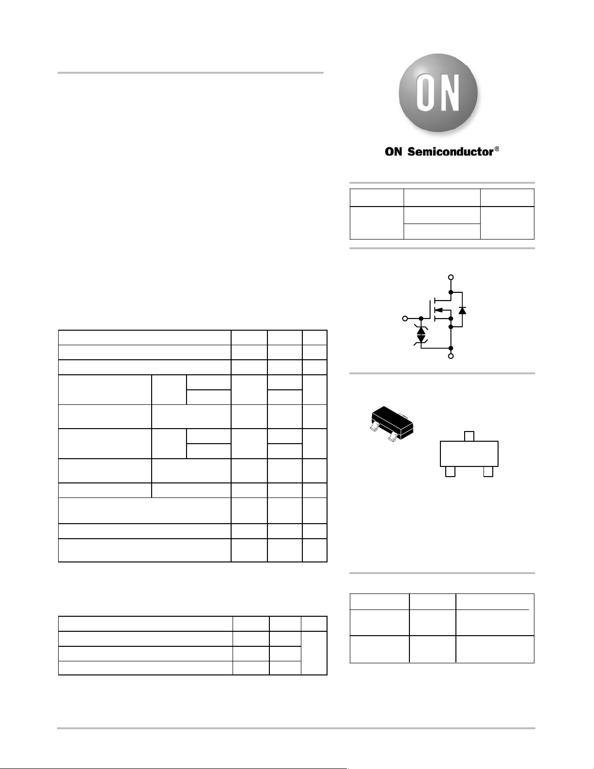
NTR4003N
Small Signal MOSFET
30 V, 0.56 A, Single N−Channel, SOT−23
Features
• Low Gate Voltage Threshold (V
Design
• Low Gate Charge for Fast Switching
• ESD Protected Gate
• SOT−23 Package Provides Excellent Thermal Performance
• Minimum Breakdown Voltage Rating of 30 V
• These are Pb−Free Devices
Applications
• Notebooks:
♦ Level Shifters
♦ Logic Switches
♦ Low Side Load Switches
• Portable Applications
MAXIMUM RATINGS (T
Parameter
Drain−to−Source Voltage V
Gate−to−Source Voltage V
Continuous Drain
Current (Note 1)
Power Dissipation
(Note 1)
Continuous Drain
Current (Note 1)
Power Dissipation
(Note 1)
Pulsed Drain Current
Operating Junction and Storage Temperature TJ,
Source Current (Body Diode) I
Lead Temperature for Soldering Purposes
(1/8” from case for 10 s)
Stresses exceeding Maximum Ratings may damage the device. Maximum
Ratings are stress ratings only. Functional operation above the Recommended
Operating Conditions is not implied. Extended exposure to stresses above the
Recommended Operating Conditions may affect device reliability.
THERMAL RESISTANCE RATINGS
Parameter Symbol Max Unit
Junction−to−Ambient − Steady State (Note 1)
Junction−to−Ambient − t < 10 s (Note 1)
Junction−to−Ambient − Steady State (Note 2)
1. Surface−mounted on FR4 board using 1 in sq pad size
(Cu area = 1.127 in sq [1 oz] including traces).
2. Surface−mounted on FR4 board using the minimum recommended pad size.
= 25°C unless otherwise noted)
J
Steady
State
Steady State P
t < 10 s
t < 5 s P
tp = 10 ms
) to Facilitate Drive Circuit
GS(TH)
Symbol Value Unit
JA
JA
JA
30 V
±20 V
0.5
0.69 W
0.56
0.83 W
1.7 A
−55 to
150
1.0 A
260 °C
180
150
300
DSS
GS
TA = 25°C
TA = 85°C 0.37
TA = 25°C
TA = 85°C 0.40
I
D
I
D
I
DM
Tstg
S
T
R
q
R
q
R
q
D
D
L
A
A
°C
°C/W
http://onsemi.com
(BR)DSS
30 V
TYP
R
DS(on)
1.0 W @ 4.0 V
1.5 W @ 2.5 V
ID MAXV
0.56 A
N−Channel
3
1
2
MARKING DIAGRAM/
PIN ASSIGNMENT
3
1
2
SOT−23
CASE 318
STYLE 21
TR8 = Specific Device Code
M = Date Code
G = Pb−Free Package
(Note: Microdot may be in either location)
*Date Code orientation and overbar may vary
depending upon manufacturing location.
3
Drain
TR8 M G
G
1
Gate2Source
ORDERING INFORMATION
Device Package Shipping
NTR4003NT1G SOT−23
(Pb−Free)
NTR4003NT3G SOT−23
(Pb−Free)
†For information on tape and reel specifications,
including part orientation and tape sizes, please
refer to our Tape and Reel Packaging Specification
Brochure, BRD8011/D.
3000/Tape & Reel
10,000/Tape & Reel
†
© Semiconductor Components Industries, LLC, 2006
May, 2006 − Rev. 0
1 Publication Order Number:
NTR4003N/D
NTR4003N
ELECTRICAL CHARACTERISTICS (T
Parameter
= 25°C unless otherwise specified)
J
Symbol Test Condition Min Typ Max Units
OFF CHARACTERISTICS
Drain−to−Source Breakdown Voltage
Drain−to−Source Breakdown Voltage
Temperature Coefficient
Zero Gate Voltage Drain Current I
Gate−to−Source Leakage Current I
V
(BR)DSS
V
(BR)DSS/TJ
DSS
GSS
VGS = 0 V, ID = 100 mA
VGS = 0 V,
V
= 30 V
DS
VDS = 0 V, VGS = ±10 V ±1.0
ON CHARACTERISTICS (Note 3)
Gate Threshold Voltage
Negative Threshold
Temperature Coefficient
Drain−to−Source On Resistance
Forward Transconductance g
V
GS(TH)
V
GS(TH)/TJ
R
DS(on)
FS
VGS = VDS, ID = 250 mA
VGS = 4.0 V, ID = 10 mA 1.0 1.5
VGS = 2.5 V, ID = 10 mA 1.5 2.0
VDS = 3.0 V, ID = 10 mA 0.33 S
CHARGES AND CAPACITANCES
Input Capacitance
Output Capacitance C
Reverse Transfer Capacitance C
Total Gate Charge Q
Threshold Gate Charge Q
Gate−to−Source Gate Charge Q
Gate−to−Drain Charge Q
C
iss
oss
rss
G(TOT)
G(TH)
GS
GD
VGS = 0 V, f = 1.0 MHz,
V
= 5.0 V
DS
V
= 5.0 V, V
GS
ID = 0.1 A
SWITCHING CHARACTERISTICS (Note 4)
Turn−On Delay Time
Rise Time t
Turn−Off Delay Time t
Fall Time t
t
d(on)
d(off)
r
f
VGS = 4.5 V, VDD = 5.0 V,
= 0.1 A, RG = 50 W
I
D
SOURCE−DRAIN DIODE CHARACTERISTICS
Forward Diode Voltage
Reverse Recovery Time t
V
SD
RR
VGS = 0 V,
I
= 10 mA
S
VGS = 0 V, dIS/dt = 8A/ms,
IS = 10 mA
3. Pulse Test: pulse width v 300 ms, duty cycle v 2%.
4. Switching characteristics are independent of operating junction temperatures.
30 V
40 mV/°C
TJ = 25°C 1.0
0.8 1.4 V
3.4 mV/°C
21
19.7
8.1
1.15
= 24 V,
DS
0.15
0.32
0.23
16.7
47.9
65.1
64.2
TJ = 25°C 0.65 0.7
TJ = 125°C 0.45
14 ns
mA
mA
W
pF
nC
ns
V
http://onsemi.com
2
 Loading...