

ON Semiconductor NTP52N10 Technical data
查询NTP52N10供应商
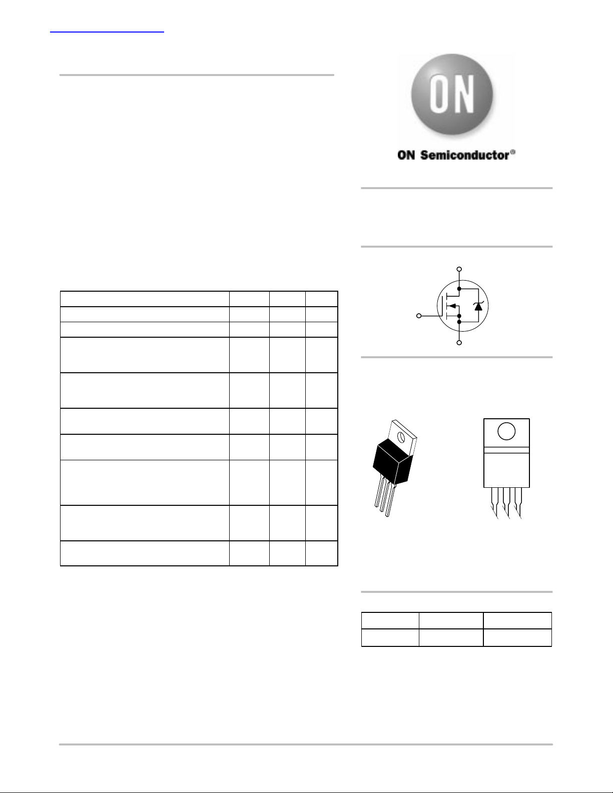
NTP52N10
Power MOSFET
52 Amps, 100 Volts
N−Channel Enhancement Mode TO−220
Features
• Source−to−Drain Diode Recovery Time comparable to a Discrete
Fast Recovery Diode
• Avalanche Energy Specified
• I
and R
DSS
T ypical Applications
• PWM Motor Controls
• Power Supplies
• Converters
MAXIMUM RATINGS (T
Drain−to−Source Voltage V
Drain−to−Source Voltage (RGS = 1.0 MΩ) V
Gate−to−Source Voltage
− Continuous
− Non−Repetitive (t
Drain− Continuous @ TA 25°C
− Continuous @ T
− Pulsed (Note 1.)
Total Power Dissipation @ TA 25°C
Derate above 25°C
Operating and Storage Temperature Range TJ, T
Single Drain−to−Source Avalanche Energy
− Starting T
(V
= 50 V, VGS = 10 Vdc,
DD
I
(pk) = 40 A, L = 1.0 mH, RG = 25 Ω)
L
Thermal Resistance
− Junction−to−Case
− Junction−to−Ambient
Maximum Lead Temperature for Soldering
Purposes, 1/8″ from case for 10 seconds
1. Pulse Test: Pulse Width = 10 µs, Duty Cycle = 2%.
Specified at Elevated Temperature
DS(on)
= 25°C unless otherwise noted)
C
Rating Symbol Value Unit
stg
100 Vdc
100 Vdc
20
40
52
40
156
178
1.43
−55 to
+150
800 mJ
0.7
62.5
260 °C
= 25°C
J
10 ms)
p
100°C
A
V
V
I
E
R
R
DSS
DGR
GS
GSM
I
D
I
D
DM
P
D
AS
θ
JC
θ
JA
T
L
Vdc
Adc
Watts
W/°C
°C
°C/W
1
2
3
http://onsemi.com
52 AMPERES
100 VOLTS
D
= 10 V
GS
S
Gate
1
30 mΩ @ V
N−Channel
G
MARKING DIAGRAM
& PIN ASSIGNMENT
4
TO−220AB
CASE 221A
STYLE 5
NTP52N10 = Device Code
LL = Location Code
Y = Year
WW = Work Week
4
Drain
NTP52N10
LLYWW
3
Source
2
Drain
Semiconductor Components Industries, LLC, 2003
December, 2003 − Rev. 2
ORDERING INFORMATION
Device Package Shipping
NTP52N10 TO−220AB 50 Units/Rail
1 Publication Order Number:
NTP52N10/D
NTP52N10
)
f = 1.0 MHz)
(V
DD
80 Vdc, I
D
Adc
)
V
GS
Vdc)
)
diS/dt = 100 A/µs)
ELECTRICAL CHARACTERISTICS (T
= 25°C unless otherwise noted)
C
Characteristic
OFF CHARACTERISTICS
Drain−to−Source Breakdown Voltage
(V
= 0 Vdc, ID = 250 µAdc)
GS
Temperature Coefficient (Positive)
Zero Gate Voltage Drain Current
= 0 Vdc, VDS = 100 Vdc, TJ =25°C)
(V
GS
= 0 Vdc, VDS = 100 Vdc, TJ =125°C)
(V
GS
Gate−Body Leakage Current (VGS = ±20 Vdc, VDS = 0 Vdc) I
ON CHARACTERISTICS
Gate Threshold Voltage
= VGS, ID = 250 µAdc)
(V
DS
Temperature Coefficient (Negative)
Static Drain−to−Source On−State Resistance
= 10 Vdc, ID = 26 Adc)
(V
GS
(V
= 10 Vdc, ID = 26 Adc, TJ = 125°C)
GS
Drain−to−Source On−Voltage
= 10 Vdc, ID = 52 Adc)
(V
GS
Forward Transconductance (VDS = 26 Vdc, ID = 10 Adc) g
DYNAMIC CHARACTERISTICS
Input Capacitance
Output Capacitance
(VDS = 25 Vdc, VGS = 0 Vdc,
f = 1.0 MHz
Transfer Capacitance
SWITCHING CHARACTERISTICS (Notes 2. & 3.)
Turn−On Delay Time
Rise Time
Turn−Off Delay Time
(V
= 80 Vdc, ID = 52 Adc,
DD
= 10 Vdc, RG = 9.1 Ω)
V
GS
52
,
Fall Time t
Gate Charge
(VDS = 80 Vdc, ID = 52 Adc,
V
= 10 Vdc
= 10
BODY−DRAIN DIODE RATINGS (Note 2.)
Diode Forward On−Voltage
(IS = 52 Adc, VGS = 0 Vdc)
(I
= 52 Adc, VGS = 0 Vdc, TJ = 125°C)
S
Reverse Recovery Time
(IS = 52 Adc, VGS = 0 Vdc,
di
/dt = 100 A/µs
Reverse Recovery Stored Charge Q
2. Indicates Pulse Test: P.W. = 300 µs Max, Duty Cycle = 2%.
3. Switching characteristics are independent of operating junction temperature.
Symbol Min Typ Max Unit
V
(BR)DSS
I
DSS
GSS
V
GS(th)
R
DS(on)
V
DS(on)
100
−
−
−
−
160
−
−
−
−
5.0
50
− − ±100 nAdc
2.0
−
−
−
2.92
−8.75
0.023
0.050
4.0
−
0.030
0.060
Vdc
mV/°C
µAdc
Vdc
mV/°C
Vdc
− 1.25 1.45
− 31 − mhos
− 2250 3150 pF
− 620 860
− 135 265
− 15 25 ns
− 95 180
− 74 150
− 100 190
− 72 135 nC
− 13 −
− 37 −
−
−
− 148 −
1.06
0.95
1.5
−
Vdc
ns
− 106 −
− 42 −
− 0.66 − µC
C
C
C
t
d(on)
t
d(off)
Q
Q
Q
V
t
t
t
FS
iss
oss
rss
t
tot
gs
gd
SD
rr
a
b
RR
r
f
Ω
http://onsemi.com
2
NTP52N10
100
VGS = 10 V
8 V
80
7 V
60
40
20
, DRAIN CURRENT (AMPS)
D
I
0
0
231
, DRAIN−TO−SOURCE VOLTAGE (VOLTS)
V
DS
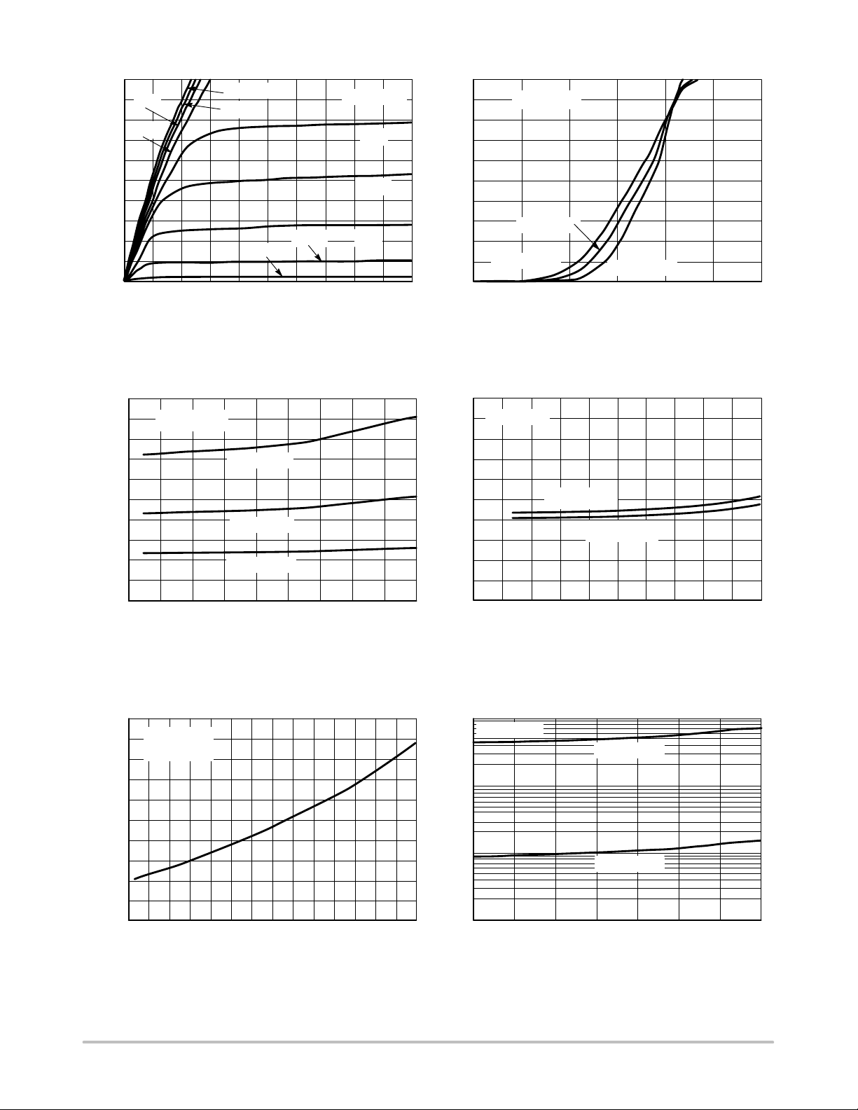
Figure 1. On−Region Characteristics Figure 2. Transfer Characteristics
0.05
VGS = 10 V
0.04
0.03
0.02
9 V
4 V
4675
TJ = 100°C
TJ = 25°C
4.5 V
TJ = 25°C
6 V
5.5 V
5 V
89
100
80
60
40
20
, DRAIN CURRENT (AMPS)
D
I
0
10
23 6
0.05
TJ = 25°C
0.04
0.03
0.02
VDS ≥ 10 V
TJ = 25°C
TJ = 100°C
TJ = −55°C
45
, GATE−TO−SOURCE VOLTAGE (VOLTS)
V
GS
VGS = 10 V
VGS = 15 V
87
0.01
TJ = −55°C
, DRAIN−TO−SOURCE RESISTANCE (Ω)
0
DS(on)
R
10
30
20 40 50 100
60 70 90
80
ID, DRAIN CURRENT (AMPS)
Figure 3. On−Resistance versus
Drain Current and Temperature
2.5
ID = 26 A
V
= 10 V
GS
2
1.5
1
(NORMALIZED)
0.5
, DRAIN−TO−SOURCE RESISTANCE
DS(on)
−60 90600−30 150
R
TJ, JUNCTION TEMPERATURE (°C)
30
120
0.01
, DRAIN−TO−SOURCE RESISTANCE (Ω)
0
DS(on)
R
0
20 40 60 10080
ID, DRAIN CURRENT (AMPS)
Figure 4. On−Resistance versus Drain Current
and Gate Voltage
10000
, LEAKAGE (nA)
I
VGS = 0 V
TJ = 150°C
1000
100
DSS
TJ = 100°C
10
30 70605040 100
80
VDS, DRAIN−TO−SOURCE VOLTAGE (VOLTS)
90
Figure 5. On−Resistance Variation with
Temperature
http://onsemi.com
Figure 6. Drain−To−Source Leakage
Current versus Voltage
3
 Loading...