

Page 1
NTP2955
&
MOSFET – Power, Single,
P-Channel, TO-220
-60 V, -12 A
Features
• Low R
DS(on)
• Rugged Performance
• Fast Switching
• These are Pb−Free Devices*
Applications
• Industrial
• Automotive
• Power Supplies
MAXIMUM RATINGS (T
Parameter
Drain−to−Source Voltage V
Gate−to−Source Voltage V
Continuous Drain
Current (Note 1)
Power Dissipation
(Note 1)
Continuous Drain
Current (Note 1)
Power Dissipation
(Note 1)
Pulsed Drain Current
Operating Junction and Storage Temperature TJ,
Source Current (Body Diode) I
Single Pulse Drain−to−Source Avalanche
Energy (VDD = −30 V, VG = −10 V,
= −12 A, L = 3.0 mH, RG = 3.0 W)
I
PK
Lead Temperature for Soldering Purposes
(1/8” from case for 10 s)
= 25°C unless otherwise noted)
J
Symbol Value Unit
Steady
State
Steady
State
TC = 25°C
TC = 85°C −9.0
TC = 25°C P
TA = 25°C
TA = 85°C −1.8
TA = 25°C P
tp =10 ms
D
D
L
−60 V
±20 V
−12
62.5 W
−2.4
2.4 W
−42 A
−55 to
175
−12 A
260 °C
DSS
GS
I
D
I
D
I
DM
T
STG
S
EAS 216 mJ
T
°C
www.onsemi.com
(BR)DSS
−60 V
DS(on)
156 mW @ −10 V
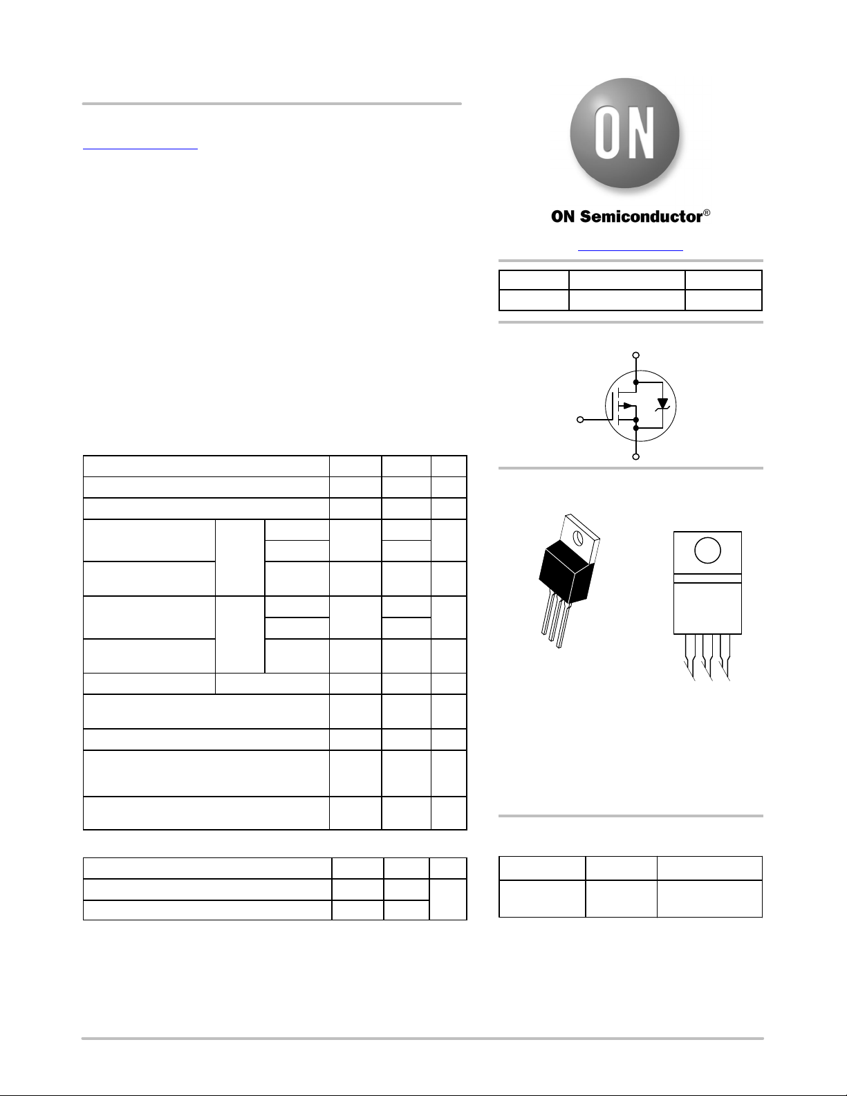
P−Channel
D
G
Typ
S
ID MAXV
−12 A
R
MARKING DIAGRAM
PIN ASSIGNMENT
A
A
1
2
3
TO−220
CASE 221A
STYLE 5
A = Assembly Location
Y = Year
WW = Work Week
G = Pb−Free Package
D
NT2955G
AYWW
1
DS
G
THERMAL RESISTANCE RATINGS
Parameter Symbol Max Unit
Junction−to−Case
Junction−to−Ambient − Steady State (Note 1)
Stresses exceeding those listed in the Maximum Ratings table may damage the
device. If any of these limits are exceeded, device functionality should not be
assumed, damage may occur and reliability may be affected.
© Semiconductor Components Industries, LLC, 2015
June, 2019 − Rev. 3
R
q
JC
R
q
JA
°C/W
2.4
62.5
1 Publication Order Number:
ORDERING INFORMATION
Device Package Shipping
NTP2955G TO−220
(Pb−Free)
50 Units / Rail
NTP2955/D
Page 2

NTP2955
1. When surface mounted to an FR4 board using 1 in pad size
(Cu. area = 1.127 in sq [1 oz] including traces).
*For additional information on our Pb−Free strategy and soldering details, please
download the ON Semiconductor Soldering and Mounting Techniques
Reference Manual, SOLDERRM/D.
www.onsemi.com
2
Page 3
NTP2955
ELECTRICAL CHARACTERISTICS (T
Parameter
=25°C unless otherwise stated)
J
Symbol Test Condition Min Typ Max Unit
OFF CHARACTERISTICS
Drain−to−Source Breakdown Voltage V
Drain−to−Source Breakdown Voltage
Temperature Coefficient
V
(BR)DSS/TJ
Zero Gate Voltage Drain Current I
Gate−to−Source Leakage Current I
(BR)DSS
DSS
GSS
V
V
V
GS
DS
V
= 0 V, I
GS
= 0 V,
= −48 V
= 0 V, V
DS
= −250 mA
D
T
T
J
= ±20 V ±100 nA
GS
ON CHARACTERISTICS (Note 2)
Gate Threshold Voltage
Negative Threshold Temperature
Coefficient
Drain−to−Source On Resistance R
Forward Transconductance g
V
GS(TH)
V
GS(TH)/TJ
DS(on)
FS
V
= VDS, ID = −250 mA
GS
V
= −10 V, I
GS
V
= −60 V, I
DS
= −12 A
D
= −12 A 6.0 S
D
CHARGES AND CAPACITANCES
Input Capacitance
Output Capacitance C
Reverse Transfer Capacitance C
Total Gate Charge Q
Threshold Gate Charge Q
Gate−to−Source Charge Q
Gate−to−Drain Charge Q
C
ISS
OSS
RSS
G(TOT)
G(TH)
GS
GD
V
= 0 V, f = 1.0 MHz,
GS
V
DS
V
= −10 V, V
GS
I
D
= −25 V
DS
= −12 A
= −48 V,
SWITCHING CHARACTERISTICS (Note 3)
Turn−On Delay Time
Rise Time t
Turn−Off Delay Time t
Fall Time t
t
d(on)
d(off)
r
f
V
GS
I
D
= −10 V, V
= −12 A, R
DD
= 9.1 W
G
= −30 V,
DRAIN−SOURCE DIODE CHARACTERISTICS
Forward Diode Voltage
Reverse Recovery Time t
Charge Time t
Discharge Time t
Reverse Recovery Charge Q
V
SD
RR
a
b
RR
V
= 0 V,
GS
I
= −12 A
S
V
= 0 V, dIS/dt = 100 A/ms,
GS
I
S
= −12 A
T
T
J
2. Pulse Test: pulse width ≤ 300 ms, duty cycle ≤ 2%.
3. Switching characteristics are independent of operating junction temperatures.
−60 V
67 mV/°C
= 25°C −1.0 mA
J
= 125°C −10
−2.0 −4.0 V
56 mV/°C
156 196
507 700
150 250
48 98
14
1.6 2.5
3.4
6.2
10 20
41 80
27 47
45 85
= 25°C −1.6 −2.0
J
= 125°C −1.36
53
42
12
126 nC
mW
pF
nC
ns
V
ns
www.onsemi.com
3
Page 4
NTP2955
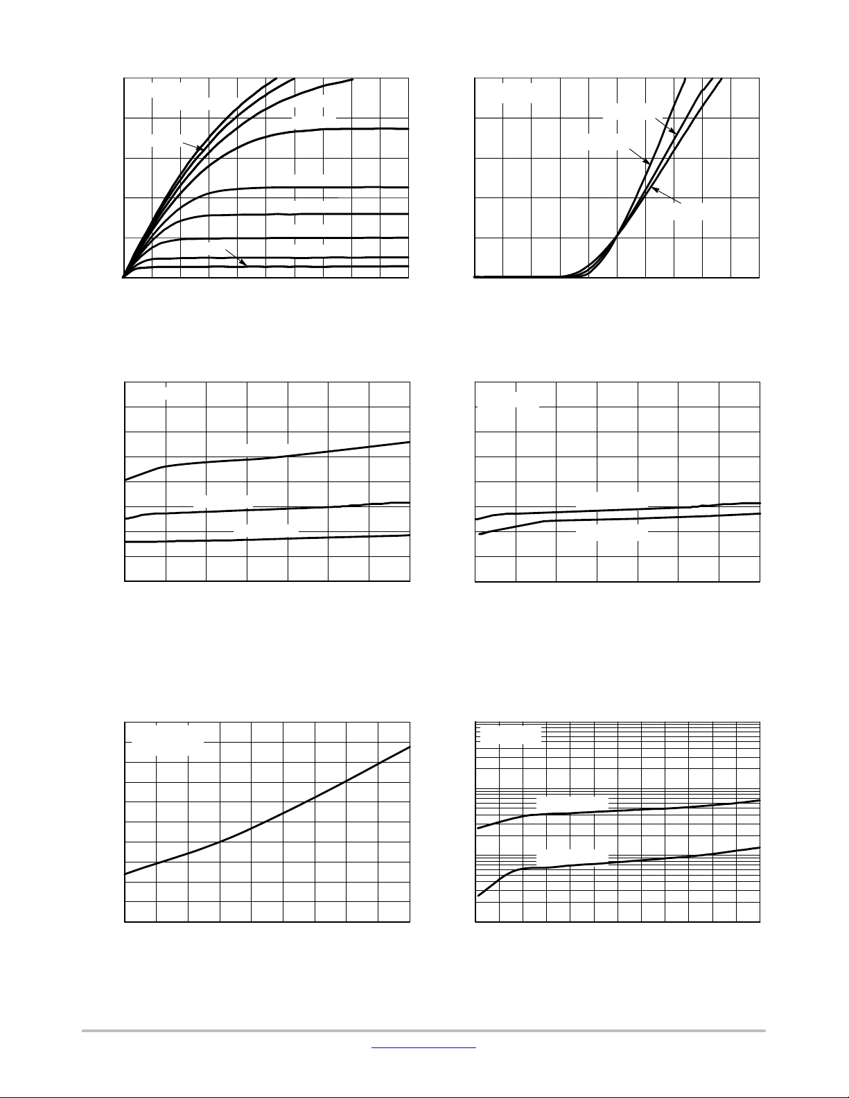
4
0
25
TJ = 25°C
VGS = −10 V
20
−9.5 V
−8.0 V
−7.0 V
15
−6.0 V
10
−5.5 V
−5.0 V
−4.5 V
, DRAIN CURRENT (A)
D
5
−I
−4.0 V
.
0
0246810
−VDS, DRAIN−TO−SOURCE VOLTAGE (V)
Figure 1. On−Region Characteristics
0.4
VGS = −10 V
0.3
T = 125°C
0.2
T = 25°C
25
VGS = −10 V
20
15
10
, DRAIN CURRENT (A)
D
5
−I
0
0246810
−VGS, GATE−TO−SOURCE VOLTAGE (V)
TJ = 25°C
TJ = 125°C
TJ = −55°C
Figure 2. Transfer Characteristics
0.4
TJ = 25°C
0.3
0.2
VGS = −10 V
0.1
, DRAIN−TO−SOURCE RESISTANCE (W)
0
DS(on)
02468101214
R
T = −55°C
−ID, DRAIN CURRENT (A)
Figure 3. On−Resistance versus Drain Current
and Temperature
2.5
ID = −12 A
= −10 V
V
GS
2.0
1.5
1.0
0.5
0
−50 −25 0 25 50 75 100 125 150 175
, DRAIN−TO−SOURCE RESISTANCE (NORMALIZED)
DS(on)
R
TJ, JUNCTION TEMPERATURE (°C)
Figure 5. On−Resistance Variation
with Temperature
0.1
, DRAIN−TO−SOURCE RESISTANCE (W)
0
DS(on)
0246810121
R
VGS = −15 V
−ID, DRAIN CURRENT (A)
Figure 4. On−Resistance versus Drain Current
and Gate Voltage
1000
VGS = 0 V
100
TJ = 125°C
, LEAKAGE (nA)
10
DSS
−I
1
0 10203040506
TJ = 100°C
−VDS, DRAIN−TO−SOURCE VOLTAGE (V)
Figure 6. Drain−to−Source Leakage
versus Voltage
www.onsemi.com
4
Page 5
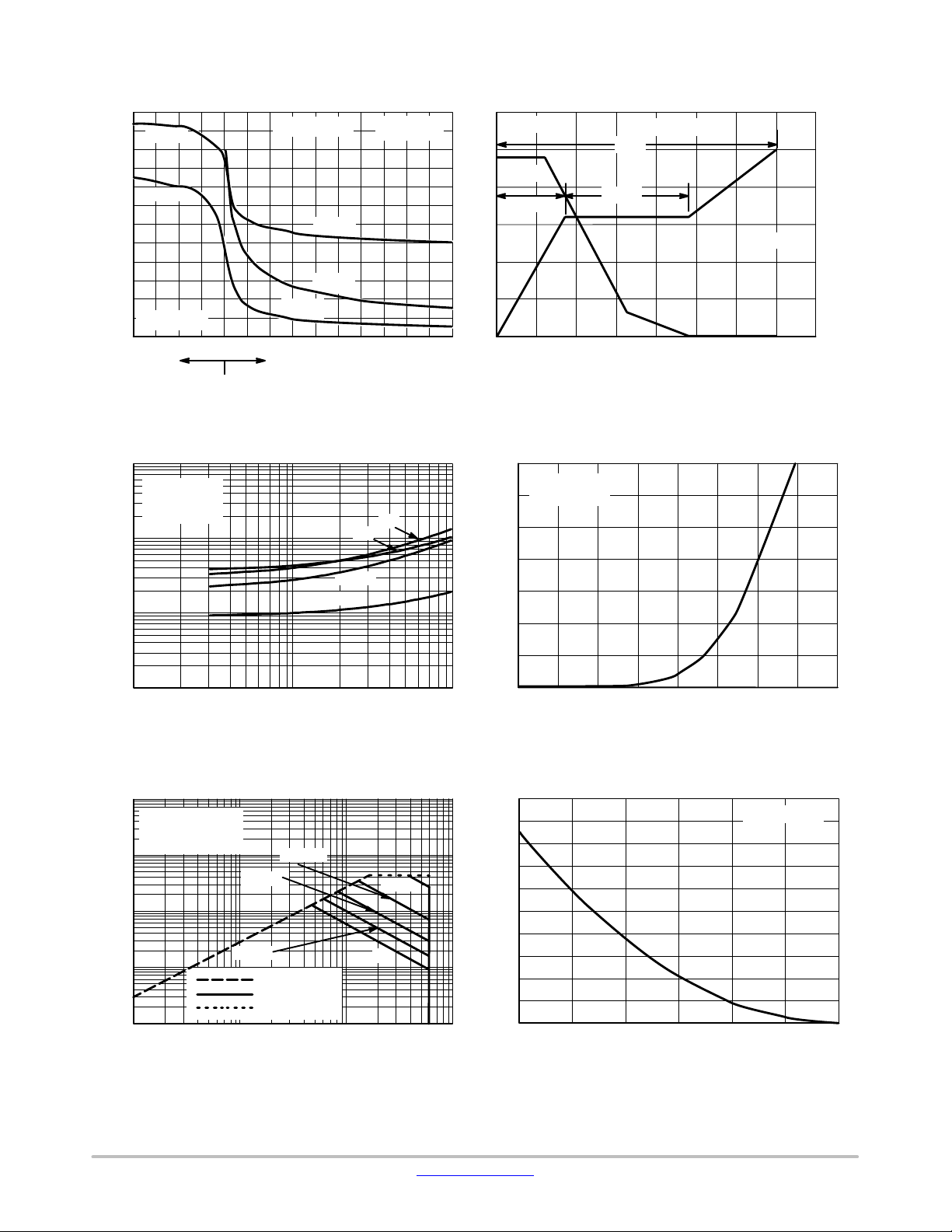
NTP2955
1200
1100
C
ISS
VGS = −0 V
TJ = 25°C
1000
900
800
C
700
600
RSS
C
ISS
500
400
300
C, CAPACITANCE (pF)
200
100
VDS = −0 V
0
−10 −5 0 5 10152025
−V
−V
GS
DS
C
OSS
C
RSS
GATE−TO−SOURCE OR DRAIN−TO−SOURCE VOLTAGE (V)
Figure 7. Capacitance Variation
1000
VDD = −30 V
= −12 A
I
D
V
= −10 V
100
t, TIME (ns)
10
GS
t
d(on)
t
d(off)
t
r
t
f
12
10
8
TJ = 25°C
V
DS
Q
GS
Q
GD
Q
ID = −12 A
T
6
V
GS
4
2
, GATE−TO−SOURCE VOLTAGE (V)
GS
0
−V
0481216
60
50
40
30
20
10
0
QG, TOTAL GATE CHARGE, (nC)
Figure 8. Gate−to−Source and
Drain−to−Source Voltage versus Total Charge
14
VGS = −0 V
12
10
8
6
4
, SOURCE CURRENT (A)
S
2
−I
= 25°C
T
J
, DRAIN−TO−SOURCE VOLTAGE (V)
DS
V
1
1 10 100
RG, GATE RESISTANCE (W)
Figure 9. Resistive Switching Time Variation
versus Gate Resistance
1000
VGS = −10 V
SINGLE PULSE
100
TJ = 25°C
1 ms
100 ms
10 ms
10
, DRAIN CURRENT (A)
1
D
−I
10 ms
R
DS(on)
LIMIT
dc
THERMAL LIMIT
0.1
PACKAGE LIMIT
0.1 1.0 10 100
−VDS, DRAIN−TO−SOURCE VOLTAGE (V)
Figure 11. Maximum Rated Forward Biased
Safe Operating Area
0
0 0.25 0.5 0.75 1.0 1.25 1.5 1.75 2.0
−VSD, SOURCE−TO−DRAIN VOLTAGE (V)
Figure 10. Diode Forward Voltage versus
Current
250
200
150
100
50
AVALANCHE ENERGY (mJ)
, SINGLE PULSE DRAIN−TO−SOURCE
AS
0
E
25 50 75 100 125 150 175
TJ, STARTING JUNCTION TEMPERATURE (°C)
Figure 12. Maximum Avalanche Energy
versus Starting Junction Temperature
ID = −12 A
www.onsemi.com
5
Page 6

MECHANICAL CASE OUTLINE
PACKAGE DIMENSIONS
SCALE 1:1
TO−220
CASE 221A−09
ISSUE AJ
DATE 05 NOV 2019
STYLE 1:
PIN 1. BASE
STYLE 5:
PIN 1. GATE
STYLE 9:
PIN 1. GATE
DOCUMENT NUMBER:
DESCRIPTION:
2. COLLECTOR
3. EMITTER
4. COLLECTOR
2. DRAIN
3. SOURCE
4. DRAIN
2. COLLECTOR
3. EMITTER
4. COLLECTOR
98ASB42148B
TO−220
STYLE 2:
PIN 1. BASE
2. EMITTER
3. COLLECTOR
4. EMITTER
STYLE 6:
PIN 1. ANODE
2. CATHODE
3. ANODE
4. CATHODE
STYLE 10:
PIN 1. GATE
2. SOURCE
3. DRAIN
4. SOURCE
STYLE 3:
PIN 1. CATHODE
2. ANODE
3. GATE
4. ANODE
STYLE 7:
PIN 1. CATHODE
2. ANODE
3. CATHODE
4. ANODE
STYLE 11:
PIN 1. DRAIN
2. SOURCE
3. GATE
4. SOURCE
Electronic versions are uncontrolled except when accessed directly from the Document Repository.
Printed versions are uncontrolled except when stamped “CONTROLLED COPY” in red.
STYLE 4:
PIN 1. MAIN TERMINAL 1
2. MAIN TERMINAL 2
3. GATE
4. MAIN TERMINAL 2
STYLE 8:
PIN 1. CATHODE
2. ANODE
3. EXTERNAL TRIP/DELAY
4. ANODE
STYLE 12:
PIN 1. MAIN TERMINAL 1
2. MAIN TERMINAL 2
3. GATE
4. NOT CONNECTED
PAGE 1 OF 1
ON Semiconductor and are trademarks of Semiconductor Components Industries, LLC dba ON Semiconductor or its subsidiaries in the United States and/or other countries.
ON Semiconductor reserves the right to make changes without further notice to any products herein. ON Semiconductor makes no warranty, representation or guarantee regarding
the suitability of its products for any particular purpose, nor does ON Semiconductor assume any liability arising out of the application or use of any product or circuit, and specifically
disclaims any and all liability, including without limitation special, consequential or incidental damages. ON Semiconductor does not convey any license under its patent rights nor the
rights of others.
© Semiconductor Components Industries, LLC, 2019
www.onsemi.com
Page 7

ON Semiconductor and are trademarks of Semiconductor Components Industries, LLC dba ON Semiconductor or its subsidiaries in the United States and/or other countries.
ON Semiconductor owns the rights to a number of patents, trademarks, copyrights, trade secrets, and other intellectual property. A listing of ON Semiconductor’s product/patent
coverage may be accessed at www.onsemi.com/site/pdf/Patent−Marking.pdf
ON Semiconductor makes no warranty, representation or guarantee regarding the suitability of its products for any particular purpose, nor does ON Semiconductor assume any liability
arising out of the application or use of any product or circuit, and specifically disclaims any and all liability, including without limitation special, consequential or incidental damages.
Buyer is responsible for its products and applications using ON Semiconductor products, including compliance with all laws, regulations and safety requirements or standards,
regardless of any support or applications information provided by ON Semiconductor. “Typical” parameters which may be provided in ON Semiconductor data sheets and/or
specifications can and do vary in different applications and actual performance may vary over time. All operating parameters, including “Typicals” must be validated for each customer
application by customer’s technical experts. ON Semiconductor does not convey any license under its patent rights nor the rights of others. ON Semiconductor products are not
designed, intended, or authorized for use as a critical component in life support systems or any FDA Class 3 medical devices or medical devices with a same or similar classification
in a foreign jurisdiction or any devices intended for implantation in the human body. Should Buyer purchase or use ON Semiconductor products for any such unintended or unauthorized
application, Buyer shall indemnify and hold ON Semiconductor and its officers, employees, subsidiaries, affiliates, and distributors harmless against all claims, costs, damages, and
expenses, and reasonable attorney fees arising out of, directly or indirectly, any claim of personal injury or death associated with such unintended or unauthorized use, even if such
claim alleges that ON Semiconductor was negligent regarding the design or manufacture of the part. ON Semiconductor is an Equal Opportunity/Affirmative Action Employer. This
literature is subject to all applicable copyright laws and is not for resale in any manner.
. ON Semiconductor reserves the right to make changes without further notice to any products herein.
PUBLICATION ORDERING INFORMATION
LITERATURE FULFILLMENT:
Email Requests to: orderlit@onsemi.com
ON Semiconductor Website: www.onsemi.com
TECHNICAL SUPPORT
North American Technical Support:
Voice Mail: 1 800−282−9855 Toll Free USA/Canada
Phone: 011 421 33 790 2910
Europe, Middle East and Africa Technical Support:
Phone: 00421 33 790 2910
For additional information, please contact your local Sales Representative
◊
www.onsemi.com
1
 Loading...