

Page 1
NTNS3193NZ
MOSFET – Single
N-Channel, Small Signal,
XLLGA3, 0.62 x 0.62 x 0.4
20 V, 224 mA
Features
• Single N−Channel MOSFET
• Ultra Small and Thin Package (0.62 x 0.62 x 0.4 mm)
• Low R
• 1.5 V Gate Voltage Rating
• These Devices are Pb−Free, Halogen Free/BFR Free and are RoHS
Compliant
Solution in 0.62 x 0.62 mm Package
DS(on)
(BR)DSS
20 V
http://onsemi.com
MOSFET
MAX ID MAXV
R
DS(on)
1.4 W @ 4.5 V
1.9 W @ 2.5 V
2.2 W @ 1.8 V
4.3 W @ 1.5 V
224 mA
Applications
• Small Signal Load Switch
• Analog Switch
• High Speed Interfacing
• Optimized for Power Management in Ultra Portable Products
MAXIMUM RATINGS (T
Parameter Symbol Value Units
Drain-to-Source Voltage V
Gate-to-Source Voltage V
Continuous Drain
Current (Note 1)
Power Dissipation (Note 1)
Pulsed Drain Current
Operating Junction and Storage
Temperature
Source Current (Body Diode) I
Lead Temperature for Soldering Purposes
(1/8″ from case for 10 s)
Stresses exceeding Maximum Ratings may damage the device. Maximum
Ratings are stress ratings only. Functional operation above the Recommended
Operating Conditions is not implied. Extended exposure to stresses above the
Recommended Operating Conditions may affect device reliability.
THERMAL RESISTANCE RATINGS
Parameter
Junction-to-Ambient – Steady State (Note 1)
Junction-to-Ambient – t ≤ 5 s (Note 1)
1. Surface Mounted on FR4 Board using the minimum recommended pad size,
(or 2 mm
2. Pulse Test: pulse width ≤ 300 ms, duty cycle ≤ 2%.
2
), 1 oz Cu.
= 25°C unless otherwise stated)
J
DSS
GS
Steady
State
t ≤ 5 s TA = 25°C 241
Steady
State
t ≤ 5 s TA = 25°C 139
TA = 25°C
TA = 85°C 162
TA = 25°C
tp = 10 ms
I
D
P
D
I
DM
TJ,
T
STG
S
T
L
Symbol Max Units
R
θJA
R
θJA
±8.0 V
224
120
673 mA
-55 to
150
120 mA
260 °C
1040
900
20 V
mA
mW
°C
°C/W
N−Channel MOSFET
D (3)
G (1)
S (2)
MARKING
DIAGRAM
3
2
1
XLLGA3
CASE 713AB
A = Specific Device Code
M = Date Code
1
A M
ORDERING INFORMATION
Device Package Shipping
NTNS3193NZT5G XLLGA3
(Pb−Free)
†For information on tape and reel specifications,
including part orientation and tape sizes, please
refer to our Tape and Reel Packaging Specifications
Brochure, BRD8011/D.
8000 /
Tape & Reel
†
© Semiconductor Components Industries, LLC, 2012
June, 2019 − Rev. 1
1 Publication Order Number:
NTNS3193NZ/D
Page 2
NTNS3193NZ
ELECTRICAL CHARACTERISTICS (T
Parameter
= 25°C unless otherwise specified)
J
Symbol Test Condition Min Typ Max Units
OFF CHARACTERISTICS
Drain-to-Source Breakdown Voltage
Drain-to-Source Breakdown Voltage
Temperature Coefficient
Zero Gate Voltage Drain Current I
Gate-to-Source Leakage Current I
V
(BR)DSS
V
(BR)DSS/TJ
DSS
GSS
VGS = 0 V, ID = 250 mA
ID = −250 mA, ref to 25°C
VGS = 0 V,
V
= 20 V
DS
VDS = 0 V, VGS = ±8.0 V ±2.0
ON CHARACTERISTICS (Note 3)
Gate Threshold Voltage
Negative Gate Threshold
Temperature Coefficient
Drain-to-Source On Resistance R
V
GS(TH)
V
GS(TH)/TJ
DS(on)
VGS = VDS, ID = 250 mA
VGS = 4.5 V, ID = 100 mA 0.65 1.4
VGS = 2.5 V, ID = 50 mA 0.9 1.9
VGS = 1.8 V, ID = 20 mA 1.1 2.2
VGS = 1.5 V, ID = 10 mA 1.4 4.3
Forward Transconductance g
Source−Drain Diode Voltage V
FS
SD
VDS = 5 V, ID = 100 mA 0.56 S
VGS = 0 V, IS = 10 mA 0.55 1.0 V
CHARGES & CAPACITANCES
Input Capacitance
Output Capacitance C
Reverse Transfer Capacitance C
Total Gate Charge Q
Threshold Gate Charge Q
Gate−to−Source Charge Q
Gate−to−Drain Charge Q
C
ISS
OSS
RSS
G(TOT)
G(TH)
GS
GD
VGS = 0 V, f = 1 MHz,
V
= 15 V
DS
VGS = 4.5 V, VDS = 15 V,
I
= 200 mA
D
SWITCHING CHARACTERISTICS, VGS = 4.5 V (Note 3)
Turn-On Delay Time
Rise Time t
Turn-Off Delay Time t
Fall Time t
t
d(ON)
r
d(OFF)
f
VGS = 4.5 V, VDD = 15 V,
= 200 mA, RG = 2 W
I
D
3. Switching characteristics are independent of operating junction temperatures.
20 V
19 mV/°C
TJ = 25°C 1.0
0.4 1.0 V
1.9 mV/°C
15.8
3.5
2.4
0.70
0.05
0.14
0.10
18
35
201
110
mA
mA
W
pF
nC
ns
http://onsemi.com
2
Page 3
NTNS3193NZ
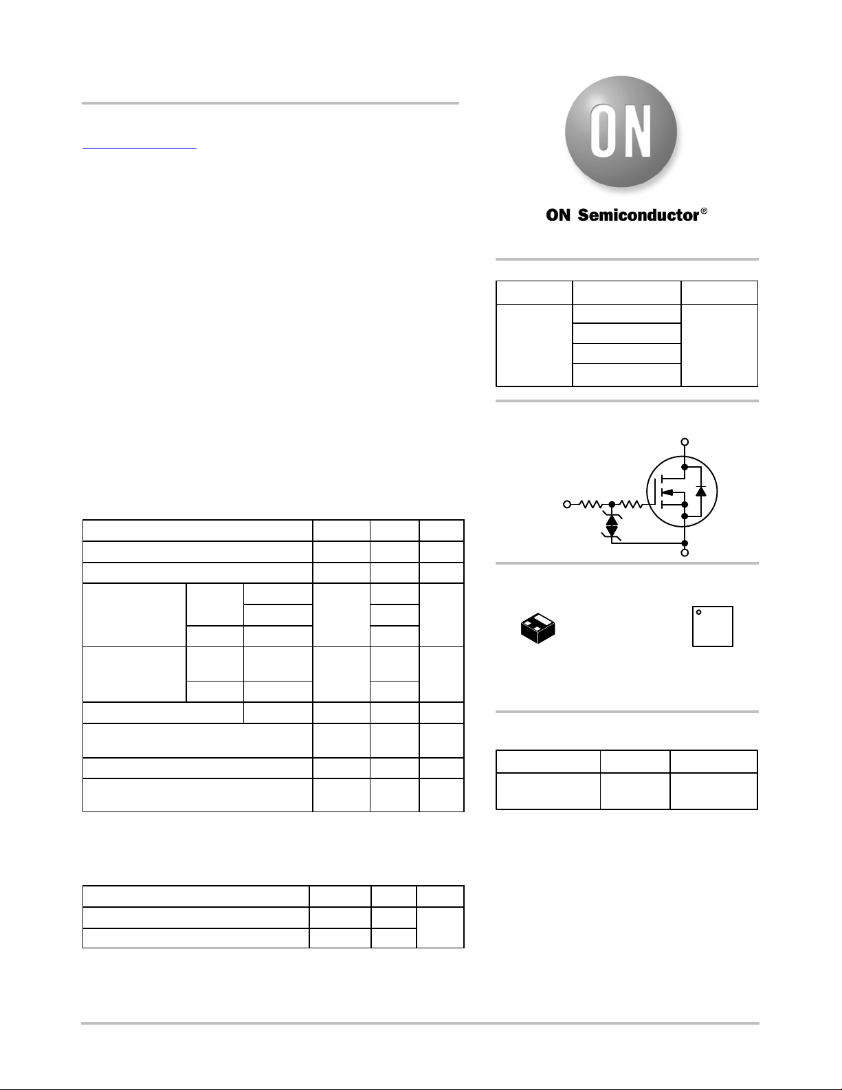
TYPICAL CHARACTERISTICS
1.0
0.9
3.5 V
0.8
4.0 V
0.7
4.5 V
0.6
0.5
0.4
0.3
, DRAIN CURRENT (A)
D
I
0.2
0.1
0
VDS, DRAIN−TO−SOURCE VOLTAGE (V) VGS, GATE−TO−SOURCE VOLTAGE (V)
VGS = 2.5 V3.0 V
Figure 1. On−Region Characteristics Figure 2. Transfer Characteristics
5.0
4.5
4.0
3.5
3.0
2.5
2.0
1.5
1.0
0.5
, DRAIN−TO−SOURCE RESISTANCE (W)
DS(on)
R
0
VGS, GATE VOLTAGE (V) ID, DRAIN CURRENT (A)
TJ = 25°C
= 0.1 A
I
D
Figure 3. On−Resistance vs. Gate−to−Source
Voltage
1.8
1.7
1.6
1.5
1.4
1.3
1.2
1.1
RESISTANCE
1.0
0.9
0.8
, NORMALIZED DRAIN−TO−SOURCE
0.7
−50 −25 0 25 50 75 100 125 150
DS(on)
R
, JUNCTION TEMPERATURE (°C)
T
J
VGS = 4.5 V
= 100 mA
I
D
VGS = 1.8 V
I
D
Figure 5. On−Resistance Variation with
Temperature
2.0 V
1.8 V
1.5 V
1.2 V
4.03.5 4.53.02.52.01.51.0
= 20 mA
1.0
0.9
0.8
0.7
0.6
0.5
0.4
0.3
, DRAIN CURRENT (A)
D
I
0.2
0.1
3.02.52.01.51.00.50
0
5.0
4.5
4.0
3.5
3.0
2.5
2.0
1.5
1.0
0.5
, DRAIN−TO−SOURCE RESISTANCE (W)
0
DS(on)
R
1000
100
, LEAKAGE (nA)
10
DSS
I
1
VDS = 5 V
TJ = −55°C
TJ = 25°C
TJ = 125°C
TJ = 25°C
VGS = 1.5 V
VGS = 1.8 V
VGS = 2.5 V
VGS = 4.5 V
0.4 0.8 0.9
Figure 4. On−Resistance vs. Drain Current and
Gate Voltage
TJ = 125°C
TJ = 85°C
820
VDS, DRAIN−TO−SOURCE VOLTAGE (V)
1816141210642
Figure 6. Drain−to−Source Leakage Current
vs. Voltage
3.02.52.01.51.00.50
1.00.70.60.50.30.20.10
http://onsemi.com
3
Page 4

30
25
20
15
10
C, CAPACITANCE (pF)
5
C
0
NTNS3193NZ
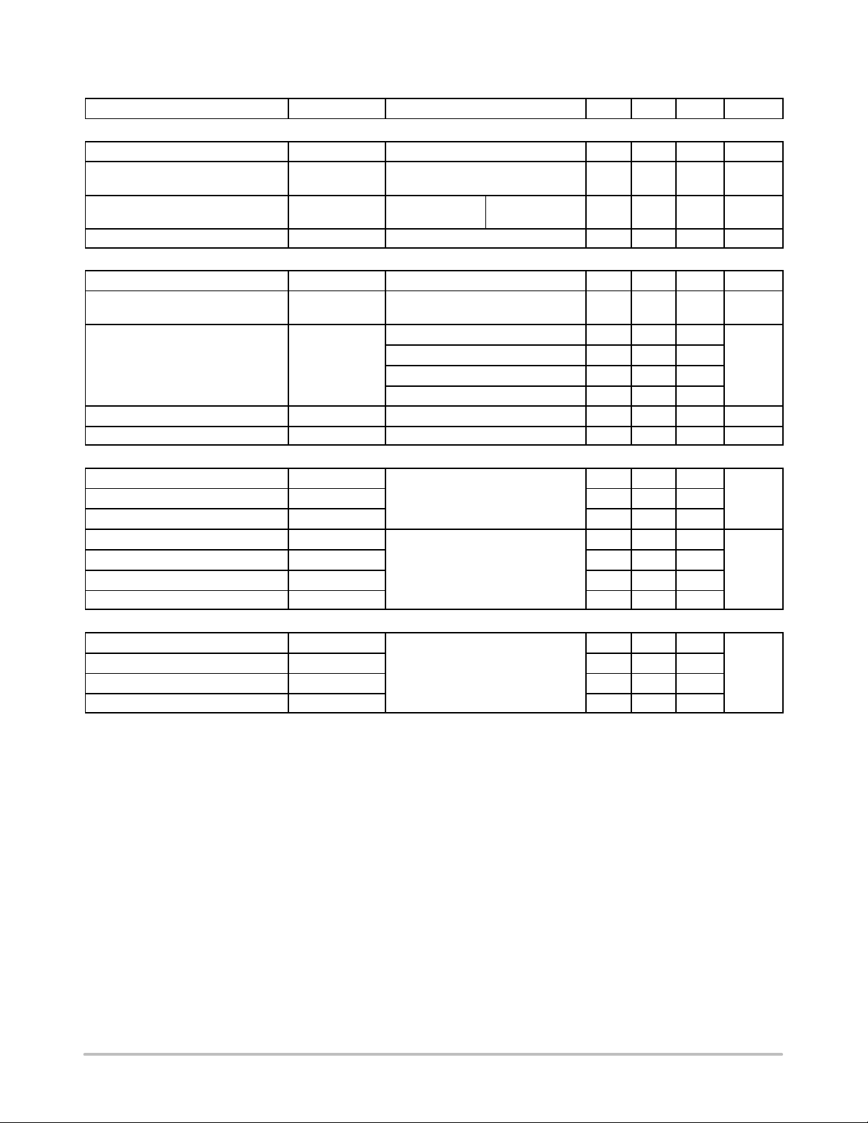
TYPICAL CHARACTERISTICS
5
VGS = 0 V
= 25°C
T
J
f = 1 MHz
C
iss
C
oss
rss
81420
181612106420
4
3
2
1
, GATE−TO−SOURCE VOLTAGE (V)
GS
0
V
V
DS
Q
GS
Q
GD
VDS, DRAIN−TO−SOURCE VOLTAGE (V) QG, TOTAL GATE CHARGE (nC)
Figure 7. Capacitance Variation Figure 8. Gate−to−Source and
Drain−to−Source Voltage vs. Total Charge
Q
T
V
GS
0.4 0.5 0.8
VDS = 15 V
= 25°C
T
J
I
= 0.2 A
D
0.70.60.30.20.10
18
15
12
9
6
3
0
DS
V
, DRAIN−TO−SOURCE VOLTAGE (V)
1000
VGS = 4.5 V
V
DD
t
d(off)
t
f
100
t, TIME (ns)
t
d(on)
t
r
10
RG, GATE RESISTANCE (W)
Figure 9. Resistive Switching Time Variation
vs. Gate Resistance
0.85
0.75
ID = 250 mA
0.65
0.55
VOLTAGE (V)
0.45
, GATE−TO−SOURCE THRESHOLD
0.35
GS(th)
−50 −25 0 25 50 75 100 125 150
V
TJ, TEMPERATURE (°C)
Figure 11. Threshold Voltage Figure 12. Maximum Rated Forward Biased
= 15 V
10
1
0.1
, SOURCE CURRENT (A)I
S
I
0.01
100101
1
0.1
0.01
, DRAIN CURRENT (A)
D
0.001
TJ = 25°C
TJ = 125°C
TJ = −55°C
0.9 1.3
V
, SOURCE−TO−DRAIN VOLTAGE (V)
SD
1.21.11.00.80.70.60.50.4
Figure 10. Diode Forward Voltage vs. Current
10 ms
100 ms
VGS ≤ 8 V
Single Pulse
T
= 25°C
C
R
DS(on)
Limit
1 ms
10 ms
dc
Thermal Limit
Package Limit
VDS, DRAIN−TO−SOURCE VOLTAGE (V)
Safe Operating Area
1001010.1
http://onsemi.com
4
Page 5

NTNS3193NZ
TYPICAL CHARACTERISTICS
1200
1100
1000
900
800
700
600
Duty Cycle = 0.5
500
(°C/W)
400
300
0.20
200
0.10
100
0
R(t), EFFECTIVE TRANSIENT THERMAL RESPONSE
0.05 0.02 0.01
1E−05 1E−04 1E−03 1E+00 1E+01 1E+02 1E+03
Figure 13. FET Thermal Response
MINIMUM RECOMMENDED
SOLDER FOOTPRINT*
2X
0.20
0.35
PITCH
*Dependent upon end user capabilities, this footprint could be used as a minimum.
Single Pulse
1E−02 1E−011E−06
t, TIME (s)
2X
0.20
1
2
DIMENSIONS: MILLIMETERS
R
q
JA Steady State
0.60
3
0.28
0.62
= 1040°C/W
http://onsemi.com
5
Page 6

MECHANICAL CASE OUTLINE
PACKAGE DIMENSIONS
SCALE 8:1
A
D3
B
E
A
SEATING
C
PLANE
D2
E2
3
L2
K
0.10 BC
0.05 C
L
PIN ONE
REFERENCE
3X
M
0.10 BC
M
0.05 C
0.10 C
C
0.10
0.10 C
0.10 C
e/2
e
b
2X
A
BOTTOM VIEW
D
TOP VIEW
A1
SIDE VIEW
2
1
2X
XLLGA3, 0.62x0.62, 0.35P
CASE 713AB
ISSUE O
M
A
M
*This information is generic. Please refer
DATE 25 SEP 2012
NOTES:
1. DIMENSIONING AND TOLERANCING PER
ASME Y14.5M, 1994.
2. CONTROLLING DIMENSION: MILLIMETERS.
MILLIMETERS
DIM MIN MAX
A 0.340 0.440
A1 0.000 0.030
b 0.100 0.200
D 0.620 BSC
D2 0.175 BSC
D3 0.205 BSC
E 0.620 BSC
E2 0.400 0.600
e 0.350 BSC
K 0.200 REF
L 0.090 0.210
L2 0.110 0.310
GENERIC
MARKING DIAGRAM*
X M
X = Specific Device Code
M = Date Code
to device data sheet for actual part
marking. Pb−Free indicator, “G”, may
or not be present.
RECOMMENDED
SOLDER FOOTPRINT*
2X
0.280
1
2X
0.200
2
0.350
PITCH
*For additional information on our Pb−Free strategy and soldering
details, please download the ON Semiconductor Soldering and
Mounting Techniques Reference Manual, SOLDERRM/D.
DOCUMENT NUMBER:
DESCRIPTION:
ON Semiconductor and are trademarks of Semiconductor Components Industries, LLC dba ON Semiconductor or its subsidiaries in the United States and/or other countries.
ON Semiconductor reserves the right to make changes without further notice to any products herein. ON Semiconductor makes no warranty, representation or guarantee regarding
the suitability of its products for any particular purpose, nor does ON Semiconductor assume any liability arising out of the application or use of any product or circuit, and specifically
disclaims any and all liability, including without limitation special, consequential or incidental damages. ON Semiconductor does not convey any license under its patent rights nor the
rights of others.
98AON84074E
XLLGA3, 0.62X0.62, 0.35P
PACKAGE
OUTLINE
0.600
3
0.350
0.760
DIMENSIONS: MILLIMETERS
Electronic versions are uncontrolled except when accessed directly from the Document Repository.
Printed versions are uncontrolled except when stamped “CONTROLLED COPY” in red.
PAGE 1 OF 1
© Semiconductor Components Industries, LLC, 2019
www.onsemi.com
Page 7

ON Semiconductor and are trademarks of Semiconductor Components Industries, LLC dba ON Semiconductor or its subsidiaries in the United States and/or other countries.
ON Semiconductor owns the rights to a number of patents, trademarks, copyrights, trade secrets, and other intellectual property. A listing of ON Semiconductor’s product/patent
coverage may be accessed at www.onsemi.com/site/pdf/Patent−Marking.pdf
ON Semiconductor makes no warranty, representation or guarantee regarding the suitability of its products for any particular purpose, nor does ON Semiconductor assume any liability
arising out of the application or use of any product or circuit, and specifically disclaims any and all liability, including without limitation special, consequential or incidental damages.
Buyer is responsible for its products and applications using ON Semiconductor products, including compliance with all laws, regulations and safety requirements or standards,
regardless of any support or applications information provided by ON Semiconductor. “Typical” parameters which may be provided in ON Semiconductor data sheets and/or
specifications can and do vary in different applications and actual performance may vary over time. All operating parameters, including “Typicals” must be validated for each customer
application by customer’s technical experts. ON Semiconductor does not convey any license under its patent rights nor the rights of others. ON Semiconductor products are not
designed, intended, or authorized for use as a critical component in life support systems or any FDA Class 3 medical devices or medical devices with a same or similar classification
in a foreign jurisdiction or any devices intended for implantation in the human body. Should Buyer purchase or use ON Semiconductor products for any such unintended or unauthorized
application, Buyer shall indemnify and hold ON Semiconductor and its officers, employees, subsidiaries, affiliates, and distributors harmless against all claims, costs, damages, and
expenses, and reasonable attorney fees arising out of, directly or indirectly, any claim of personal injury or death associated with such unintended or unauthorized use, even if such
claim alleges that ON Semiconductor was negligent regarding the design or manufacture of the part. ON Semiconductor is an Equal Opportunity/Affirmative Action Employer. This
literature is subject to all applicable copyright laws and is not for resale in any manner.
. ON Semiconductor reserves the right to make changes without further notice to any products herein.
PUBLICATION ORDERING INFORMATION
LITERATURE FULFILLMENT:
Email Requests to: orderlit@onsemi.com
ON Semiconductor Website: www.onsemi.com
TECHNICAL SUPPORT
North American Technical Support:
Voice Mail: 1 800−282−9855 Toll Free USA/Canada
Phone: 011 421 33 790 2910
Europe, Middle East and Africa Technical Support:
Phone: 00421 33 790 2910
For additional information, please contact your local Sales Representative
◊
www.onsemi.com
1
 Loading...