

ON Semiconductor NTMS7N03R2 Technical data

查询NTMS7N03R2供应商
NTMS7N03R2
Power MOSFET
7 Amps, 30 Volts
N-Channel SO-8
Features
• Ultra Low R
• Higher Efficiency Extending Battery Life
• Logic Level Gate Drive
• Miniature SO-8 Surface Mount Package
• Avalanche Energy Specified
• I
Specified at Elevated Temperature
DSS
T ypical Applications
• DC-DC Converters
• Power Management
• Motor Controls
• Inductive Loads
• Replaces MMSF7N03HD, MMSF7N03Z, and MMSF5N03HD in
Many Applications
DS(on)
http://onsemi.com
7 AMPERES
30 VOLTS
= 23 m
N-Channel
D
G
R
DS(on)
MAXIMUM RATINGS (T
Rating Symbol Value Unit
Drain-to-Source Voltage V
Drain-to-Gate Voltage (RGS = 1.0 MΩ) V
Gate-to-Source Voltage - Continuous V
Thermal Resistance - Junction to Ambient
(Note 1)
Total Power Dissipation @ TA = 25°C P
Drain Current - Continuous @ TA = 25°C
Drain Current - Continuous @ T
Drain Current - Pulsed (Note 4)
Thermal Resistance - Junction to Ambient
(Note 2)
Total Power Dissipation @ TA = 25°C P
Drain Current - Continuous @ TA = 25°C
Drain Current - Continuous @ T
Drain Current - Pulsed (Note 4)
Thermal Resistance - Junction to Ambient
(Note 3)
Total Power Dissipation @ TA = 25°C P
Drain Current - Continuous @ TA = 25°C
Drain Current - Continuous @ T
Drain Current - Pulsed (Note 4)
Operating and Storage Temperature Range TJ, T
Single Pulse Drain-to-Source Avalanche
Energy - Starting T
(V
= 30 Vdc, VGS = 10 Vdc, Peak
DD
I
= 12 Apk, L = 4.0 mH, RG = 25 Ω)
L
1. 2″ SQ. FR-4 PCB mounting, (2 oz. Cu 0.06″ thick single sided), 10 Sec. Max.
2. 2″ SQ. FR-4 PCB mounting, (2 oz. Cu 0.06″ thick single sided),
t = steady state.
3. Minimum FR4 or G10 PCB, t = steady state.
4. Pulse test: Pulse Width = 300 µs, Duty Cycle = 2%.
= 25°C unless otherwise noted)
C
= 70°C
A
= 70°C
A
= 70°C
A
= 25°C
J
R
R
R
E
DSS
DGR
GS
θ
I
I
I
DM
θ
I
I
I
DM
θ
I
I
I
DM
AS
30 Vdc
30 Vdc
± 20 Vdc
JA
D
D
D
JA
D
D
D
JA
D
D
D
stg
50 °C/W
2.5 Watts
8.5
6.8
25
85 °C/W
1.47 Watts
6.5
5.2
18
156 °C/W
0.8 Watts
4.8
3.8
14
- 55 to
+150
288 mJ
Adc
Apk
Adc
Apk
Adc
Apk
°C
S
MARKING
DIAGRAM
SO-8
8
1
CASE 751
STYLE 13
E7N03 = Device Code
A = Assembly Location
Y = Year
WW = Work Week
E7N03
AYWW
PIN ASSIGNMENT
N-C
Source
Source
Gate
1
2
3
4
Top View
Drain
8
Drain
7
Drain
6
5
Drain
ORDERING INFORMATION
Device Package Shipping
NTMS7N03R2 SO-8 2500/Tape & Reel
Semiconductor Components Industries, LLC, 2002
November, 2002 - Rev. 3
1
Publication Order Number:
NTMS7N03R2/D
NTMS7N03R2
)
f = 1.0 MHz)
R
G
9.1 Ω) (Note 5)
R
G
9.1 Ω) (Note 5)
(V
DS
Vdc, I
D
Adc
(I
S
Adc, V
GS
Vdc
ELECTRICAL CHARACTERISTICS (T
= 25°C unless otherwise noted)
C
Characteristic Symbol Min Typ Max Unit
OFF CHARACTERISTICS
Drain-to-Source Breakdown Voltage (Notes 5 and 7)
= 0 Vdc, ID = 0.25 mAdc)
(V
GS
Temperature Coefficient (Positive)
Zero Gate Voltage Drain Current
(V
= 30 Vdc, VGS = 0 Vdc)
DS
= 30 Vdc, VGS = 0 Vdc, TJ = 125°C)
(V
DS
Gate-Body Leakage Current (VGS = ± 20 Vdc, VDS = 0) I
ON CHARACTERISTICS
Gate Threshold Voltage (Note 5)
= VGS, ID = 0.25 mAdc)
(V
DS
Threshold Temperature Coefficient (Negative)
Static Drain-to-Source On-Resistance (Notes 5 and 7)
(V
= 10 Vdc, ID = 7.0 Adc)
GS
(V
= 4.5 Vdc, ID = 3.5 Adc)
GS
Drain-to-Source On-Voltage (VGS = 10 Vdc, ID = 5.0 Adc) (Notes 5 and 7) V
Forward Transconductance (VDS = 15 Vdc, ID = 2.0 Adc) (Note 5) g
DYNAMIC CHARACTERISTICS
Input Capacitance
Output Capacitance
(VDS = 25 Vdc, VGS = 0 Vdc,
f = 1.0 MHz
Transfer Capacitance
SWITCHING CHARACTERISTICS (Note 6)
Turn-On Delay Time
(V
= 10 Vdc, ID = 5.0 Adc,
Rise Time
Turn-Off Delay Time
DD
VGS = 4.5 Vdc,
= 9.1 Ω) (Note 5)
R
G
Fall Time
Turn-On Delay Time t
(V
= 10 Vdc, ID = 5.0 Adc,
Rise Time
Turn-Off Delay Time
DD
VGS = 10 Vdc,
= 9.1 Ω) (Note 5)
R
G
Fall Time
Gate Charge
(VDS = 16 Vdc, ID = 5.0 Adc,
16
V
= 10 Vdc) (Note 5)
GS
5.0
,
SOURCE-DRAIN DIODE CHARACTERISTICS
Forward On-Voltage (Note 5)
(IS = 7.0 Adc, VGS = 0 Vdc) (Note 5)
= 7.0 Adc, VGS = 0 Vdc,
(I
S
= 125°C)
T
J
Reverse Recovery Time
(IS = 7.0 Adc, VGS = 0 Vdc,
7.0
dI
/dt = 100 A/µs) (Note 5)
S
0
,
Reverse Recovery Stored Charge Q
5. Pulse Test: Pulse Width ≤300 µs, Duty Cycle ≤ 2%.
6. Switching characteristics are independent of operating junction temperature.
7. Reflects Typical Values.
Max limit Typ
Cpk
3
V
(BR)DSS
I
DSS
GSS
V
GS(th)
R
DS(on)
DS(on)
C
C
C
t
d(on)
t
d(off)
d(on)
t
d(off)
Q
Q
Q
Q
V
t
t
t
FS
iss
oss
rss
t
r
t
f
t
r
t
f
SD
rr
a
b
RR
30
-
41
-
-
-
mV/°C
µAdc
Vdc
-
-
0.02
-
1.0
10
- - 100 nAdc
Vdc
1.0
-
1.6
4.0
3.0
-
mV/°C
m
-
-
18.6
23.5
23
28
- 93 115 mV
3.0 13 - Mhos
- 1064 1190 pF
- 300 490
- 94 120
- 15 30
ns
- 71 185
- 27 70
- 38 80
- 8.0 -
- 38 -
- 33 -
- 49
T
1
2
3
- 26 43
- 3.1 -
- 6.0 -
- 5.5 -
-
-
0.82
0.67
1.1
-
- 27 -
nC
Vdc
ns
- 15 -
- 11.5 -
- 0.02 - µC
http://onsemi.com
2
NTMS7N03R2
ATTRIBUTES
Characteristics Value
ESD Protection Human Body Model
Machine Model
Charged Device Model
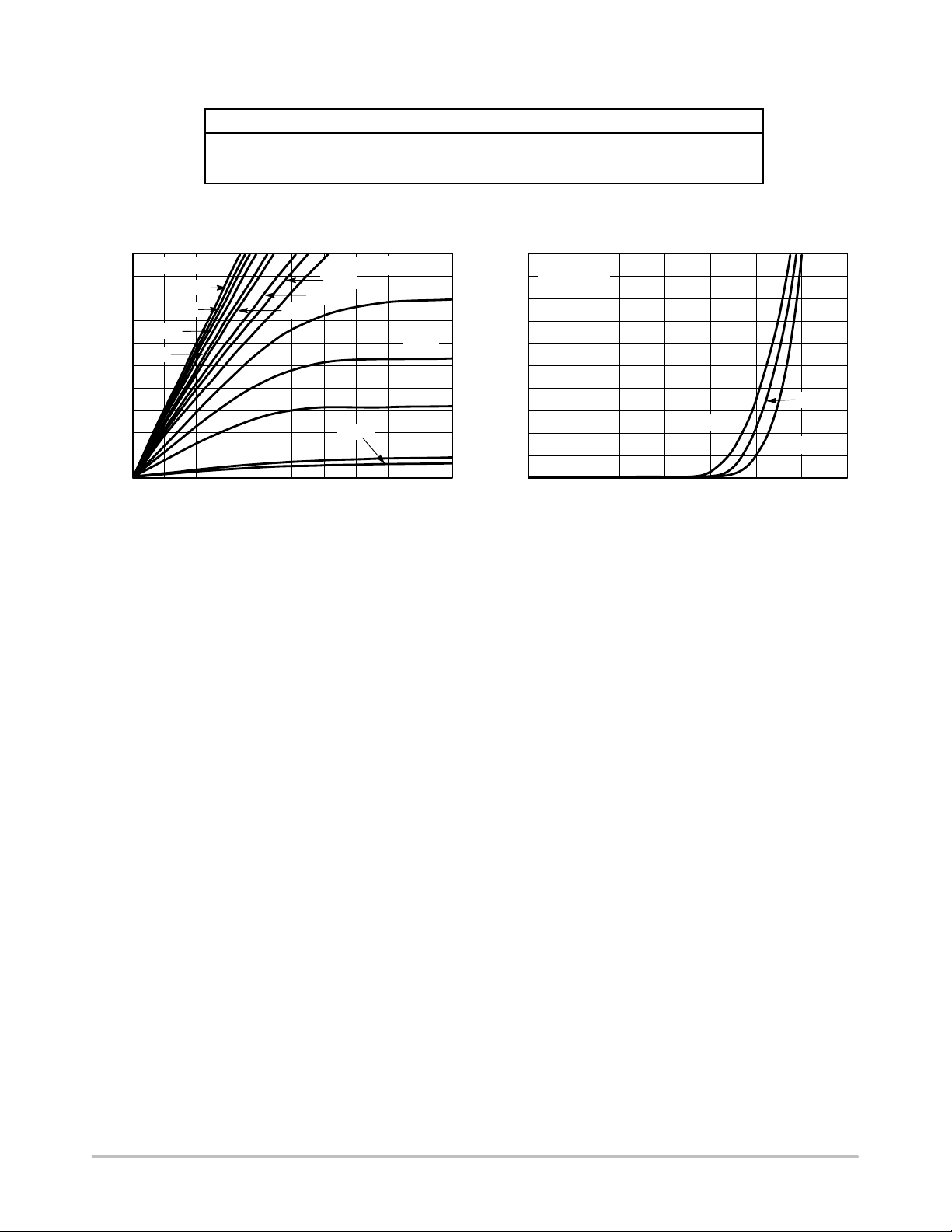
TYPICAL ELECTRICAL CHARACTERISTICS
Class 1E
Class A
Class 0
20
18
16
14
12
10
, DRAIN CURRENT (AMPS)
D
I
VGS = 10 V
8 V
7 V
6 V
5 V
8
6
4
2
0
0 0.1 0.2 0.3 1
V
, DRAIN-TO-SOURCE VOLTAGE (VOLTS)
DS
0.4 0.5
3.6 V
3.8 V
4 V
4.6 V
TJ = 25°C
2.4 V
0.8 0.9
Figure 1. On-Region Characteristics
3.4 V
3.2 V
3 V
2.8 V
10
9
VDS = 10 V
8
7
6
5
4
3
, DRAIN CURRENT (AMPS)
2
D
I
1
0
0 0.5 1 3.5
VGS, GATE-TO-SOURCE VOLTAGE (VOLTS)
TJ = 100°C
1.50.6 0.7 2
-55°C
2.5 3
Figure 2. Transfer Characteristics
25°C
http://onsemi.com
3
NTMS7N03R2
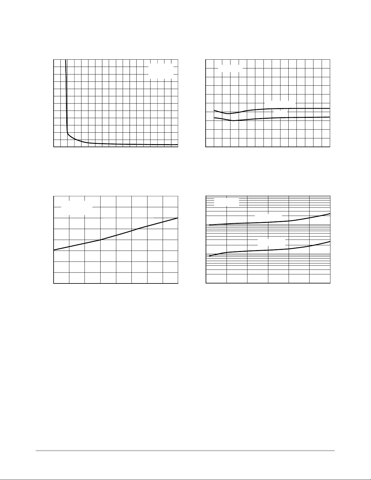
TYPICAL ELECTRICAL CHARACTERISTICS
0.6
0.5
0.4
0.3
0.2
0.1
0
, DRAIN-TO-SOURCE RESISTANCE (OHMS)
13 957
DS(on)
R
24 10
, GATE-TO-SOURCE VOLTAGE (VOLTS)
V
GS
Figure 3. On-Resistance versus
68
Gate-T o-Source Voltage
2
VGS = 10 V
= 3.5 A
I
D
1.5
ID = 3.5 A
T
= 25°C
J
0.05
TJ = 25°C
0.04
0.03
VGS = 4.5 V
0.02
0.01
0
, DRAIN-TO-SOURCE RESISTANCE (OHMS)
0 5 10 15
DS(on)
R
Figure 4. On-Resistance versus Drain Current
ID, DRAIN CURRENT (AMPS)
10 V
and Gate Voltage
1000
VGS = 0 V
TJ = 125°C
100
1
(NORMALIZED)
0.5
, DRAIN-TO-SOURCE RESISTANCE
DS(on)
0
R
-50-250 25 50 75 100 125 150
, JUNCTION TEMPERATURE (°C)
T
J
Figure 5. On-Resistance Variation with
Temperature
TJ = 100°C
, LEAKAGE (nA)
10
DSS
I
1
0102030
VDS, DRAIN-TO-SOURCE VOLTAGE (VOLTS)
Figure 6. Drain-To-Source Leakage
Current versus Voltage
http://onsemi.com
4
 Loading...