

ON Semiconductor NTMS4404N Technical data
查询NTMS4404供应商
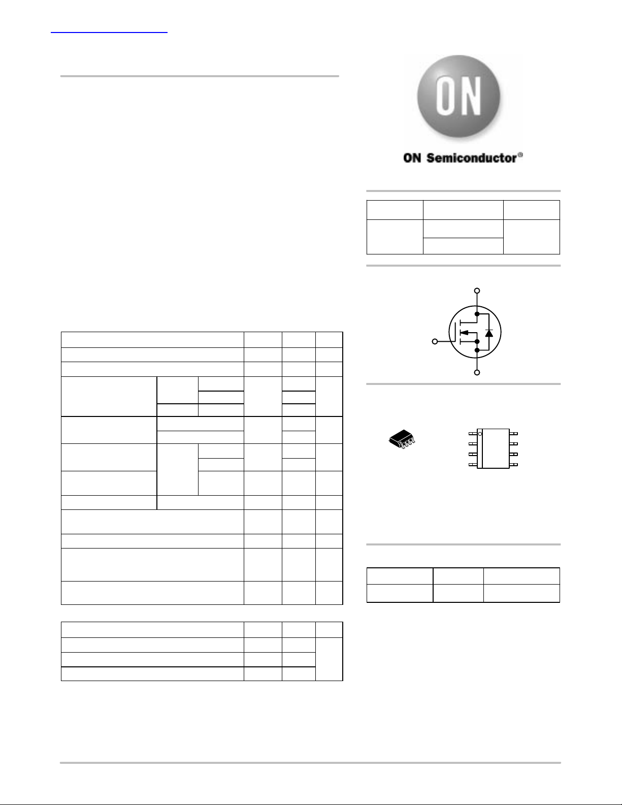
NTMS4404N
Power MOSFET
30 V, 12 A, Single N−Channel, SO−8
Features
• High Density Power MOSFET with Ultra Low R
Efficiency
• Miniature SO−8 Surface Mount Package Saving Board Space
• I
Specified at Elevated Temperature
DSS
• Diode Exhibits High Speed, Soft Recovery
Applications
• Power Management for Battery Power Products
• Portable Products
• Computers, Printers, PCMCIA Cards
• Cell Phones, Cordless Telephones
DS(on)
for Higher
(BR)DSS
30 V
http://onsemi.com
TYP
R
DS(on)
9.7 m @ 10 V
15.5 m @ 4.5 V
N−Channel
D
ID MAXV
12 A
MAXIMUM RATINGS (T
Parameter
Drain−to−Source Voltage V
Gate−to−Source Voltage V
Continuous Drain
Current (Note 1) State
Power Dissipation
(Note 1)
Continuous Drain
Current (Note 2) State
Power Dissipation
(Note 2)
Pulsed Drain Current tp = 10 s, DC = 2 % I
Operating Junction and Storage Temperature TJ,
Source Current (Body Diode) I
Single Pulse Drain−to−Source Avalanche
Energy (VDD = 20 V, VGS = 5 V, IPK = 7.25 A,
L = 19 mH, R
Lead Temperature for Soldering Purposes
(1/8” from case for 10 s)
= 25 )
G
= 25°C unless otherwise stated)
J
Symbol Value Unit
DSS
GS
Steady
tp 10 s TA = 25°C 12
Steady
TA = 25°C
TA = 70°C 7.6
Steady State
tp 10 s 2.5
TA = 25°C
TA = 70°C 5.6
TA = 25°C P
T
P
E
I
D
D
I
D
D
DM
STG
S
AS
T
L
30 V
20 V
9.6
1.56
7.0
0.83 W
50 A
−55 to
150
6.0 A
500 mJ
260 °C
A
W
A
°C
THERMAL RESISTANCE RATINGS
Parameter Symbol Max Unit
Junction−to−Ambient – Steady State (Note 1) R
Junction−to−Ambient – t = 1 0 s (Note 1) R
Junction−to−Ambient – Steady State (Note 2) R
1. Surface−mounted on FR4 board using 1 in sq. pad size
(Cu area = 1.127 in sq. [1 oz] including traces)
2. Surface−mounted on FR4 board using the minimum recommended pad
size (Cu area = 0.412 in sq.)
JA
JA
JA
80
50
150
°C/W
G
S
MARKING DIAGRAM/
PIN ASSIGNMENT
18
E4404N
1
SO−8
CASE 751
STYLE 12
Source
Source
Source
Gate
E4404N= Device Code
L = Assembly Location
Y = Year
WW = Work Week
LYWW
Top View
Drain
Drain
Drain
Drain
ORDERING INFORMATION
Device Package Shipping
NTMS4404NR2 SO−8 2500/Tape & Reel
†For information on tape and reel specifications,
including part orientation and tape sizes, please
refer to our Tape and Reel Packaging Specification
Brochure, BRD8011/D.
†
Semiconductor Components Industries, LLC, 2003
November, 2003 − Rev. 1
1 Publication Order Number:
NTMS4404N/D
NTMS4404N
()
GS
,,
DS
V
GS
V
DS
I
D
V
GS
V
DS
I
D
V
GS
d
ISD/dt
100 A/s
ELECTRICAL CHARACTERISTICS (T
Parameter
= 25°C unless otherwise specified)
J
Symbol Test Condition Min Typ Max Units
OFF CHARACTERISTICS
Drain−to−Source Breakdown Voltage V
Drain−to−Source Breakdown Voltage
V
Temperature Coefficient
Zero Gate Voltage Drain Current I
Gate−to−Source Leakage Current I
(BR)DSS
(BR)DSS
T
J
DSS
GSS
/
VGS = 0 V, ID = 250 A 30 V
VGS = 0 V, VDS = 30 V
VDS = 0 V, VGS = 20 V 100 nA
ON CHARACTERISTICS (Note 3)
Gate Threshold Voltage
Gate Threshold Temperature Coefficient V
Drain−to−Source On Resistance R
V
GS(TH)
GS(TH)/TJ
DS(on)
VGS = VDS, ID = 250 A 1.0 2.2 3.0 V
VGS = 10 V, ID = 12 A 9.7 11.5
VGS = 4.5 V, ID = 6.0 A 15.5 17.5
Forward Transconductance g
FS
VDS = 15 V, ID = 12 A 17.5 S
CHARGES AND CAPACITANCES
Input Capacitance
Output Capacitance C
Reverse Transfer Capacitance C
Total Gate Charge Q
Threshold Gate Charge Q
Gate−to−Source Charge Q
Gate−to−Drain Charge Q
C
ISS
OSS
RSS
G(TOT)
G(TH)
GS
GD
V
= 0 V, f = 1 MHz, V
GS
VGS = 10 V, VDS = 24 V, ID = 12 A
SWITCHING CHARACTERISTICS, VGS = 10 V (Note 4)
Turn−On Delay Time
Rise Time tr
Turn−Off Delay Time t
Fall Time t
t
d(ON)
d(OFF)
f
V
= 10 V, VD = 24 V, ID = 12 A,
= 10 V,
RG = 2.5
SWITCHING CHARACTERISTICS, VGS = 4.5 V (Note 4)
Turn−On Delay Time
Rise Time tr
Turn−Off Delay Time t
Fall Time t
t
d(ON)
d(OFF)
f
V
= 4.5 V, VD = 24 V, ID = 6.0 A,
= 4.5 V,
RG = 2.5
DRAIN−SOURCE DIODE CHARACTERISTICS (Note 4)
Forward Diode Voltage
Reverse Recovery Time t
Charge Time t
Discharge Time tb
Reverse Recovery Charge Q
V
SD
RR
a
RR
VGS = 0 V, IS = 6.0 A
VGS = 0 V, d
0 V,
ISD/dt
I
= 6.0 A
S
NOTES:
3. Pulse Test: pulse width 300 s, duty cycle 2%.
4. Switching characteristics are independent of operating junction temperatures.
TJ = 25°C 1.0
TJ = 100°C 5.0
= 24 V
DS
= 24 V,
= 24 V,
= 12 A,
= 6.0 A,
TJ = 25°C 0.80 1.1
TJ = 125°C 0.65
= 100 A/s,
,
25 mV/°C
A
−5.0 mV/°C
m
1975 2500
pF
575 750
180 300
50 70
nC
2.4
7.5
16
15 25
ns
25 50
35 55
15 30
20
ns
80
25
15
V
40 55
ns
23
17
0.05 C
http://onsemi.com
2
 Loading...