

Page 1
NTMS4176P
Power MOSFET
-30 V, -9.6 A, P-Channel, SOIC-8
Features
•Low R
•Low Capacitance to Minimize Driver Losses
•Optimized Gate Charge to Minimize Switching Losses
•SOIC-8 Surface Mount Package Saves Board Space
•This is a Pb-Free Device
Applications
•Load Switches
•Notebook PC's
•Desktop PC's
MAXIMUM RATINGS (T
Drain-to-Source Voltage V
Gate-to-Source Voltage V
Continuous Drain
Current R
Power Dissipation
(Note 1)
R
q
JA
Continuous Drain
Current R
Power Dissipation
(Note 2)
R
q
JA
Continuous Drain
Current R
(Note 1)
Power Dissipation
t < 10 s (Note 1)
R
q
JA
Pulsed Drain Current T
Operating Junction and Storage Temperature TJ, T
Source Current (Body Diode) I
Single Pulse Drain-to-Source Avalanche
Energy T
= 15 Apk, L = 1.0 mH, RG = 25 W
I
L
Lead Temperature for Soldering Purposes
(1/8″ from case for 10 s)
Stresses exceeding Maximum Ratings may damage the device. Maximum
Ratings are stress ratings only. Functional operation above the Recommended
Operating Conditions is not implied. Extended exposure to stresses above the
Recommended Operating Conditions may affect device reliability.
1. Surface-mounted on FR4 board using 1 inch sq pad size, 1 oz Cu.
2. Surface-mounted on FR4 board using the minimum recommended pad size.
) to Minimize Conduction Losses
DS(on
= 25°C unless otherwise stated)
J
Rating Symbol Value Unit
T
= 25°C
(Note 1)
q
JA
(Note 2)
q
JA
Steady
State
t < 10 s
q
JA
= 25°C, VDD = 30 V, VGS = 10 V,
J
A
T
= 70°C -5.8
A
T
= 25°C P
A
T
= 25°C
A
T
= 70°C -4.4
A
T
= 25°C P
A
T
= 25°C
A
T
= 70°C -7.7
A
T
= 25°C P
A
= 25°C,
A
= 10 ms
t
p
STG
-30 V
±25 V
-7.3
1.44 W
-5.5
0.81 W
-9.6
2.5 W
-39 A
-55 to
+150
-2.1 A
A
A
A
°C
DSS
I
I
I
I
DM
GS
D
D
D
D
D
D
S
EAS 112.5 mJ
T
L
260 °C
http://onsemi.com
R
V
(BR)DSS
-30 V
18 mW @ -10 V
DS(on)
Max
I
Max
D
-9.6 A
30 mW @ -4.5 V
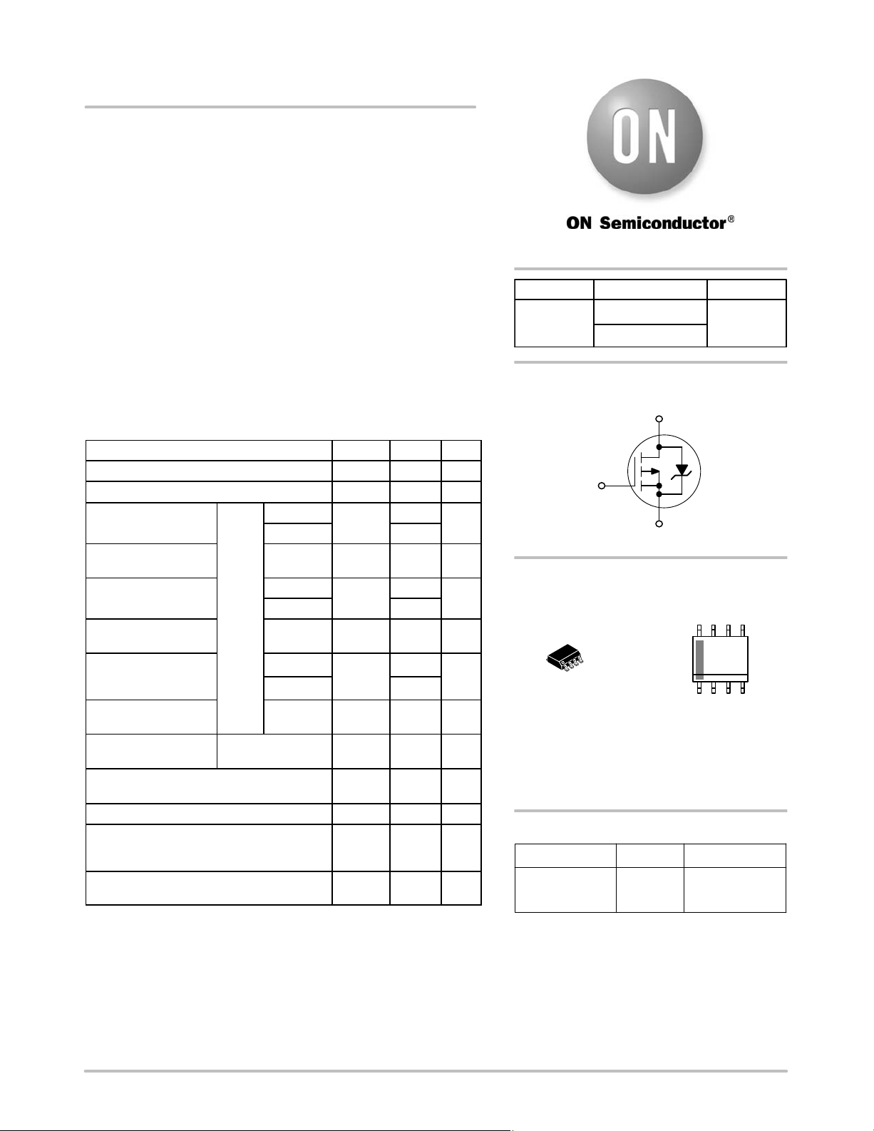
P-Channel
D
G
S
MARKING DIAGRAM
& PIN ASSIGNMENT
DDDD
8
8
1
SOIC-8
CASE 751
STYLE 12
4176P
AYWW
G
1
SSSG
4176P = Device Code
A = Assembly Location
Y = Year
WW = Work Week
G = Pb-Free Package
ORDERING INFORMATION
Device Package Shipping
NTMS4176PR2G SOIC-8
2500/Tape & Reel
(Pb-Free)
†For information on tape and reel specifications,
including part orientation and tape sizes, please
refer to our Tape and Reel Packaging Specification
Brochure, BRD8011/D.
†
© Semiconductor Components Industries, LLC, 2008
March, 2008 - Rev. 0
1 Publication Order Number:
NTMS4176P/D
Page 2
NTMS4176P
THERMAL RESISTANCE RATINGS
Rating Symbol Max Unit
Junction-to-Ambient – Steady State (Note 3)
Junction-to-Ambient – t≤10 s (Note 3)
Junction-to-FOOT (Drain)
Junction-to-Ambient – Steady State (Note 4)
3. Surface-mounted on FR4 board using 1 inch sq pad size, 1 oz Cu.
4. Surface-mounted on FR4 board using the minimum recommended pad size.
R
q
JA
R
q
JA
R
q
JF
R
q
JA
87
50
22
154
°C/W
ELECTRICAL CHARACTERISTICS (T
= 25°C unless otherwise noted)jk
J
Characteristic Symbol Test Condition Min Typ Max Unit
OFF CHARACTERISTICS
Drain-to-Source Breakdown Voltage
Drain-to-Source Breakdown Voltage Tem‐
perature Coefficient
Zero Gate Voltage Drain Current I
Gate-to-Source Leakage Current I
V
(BR)DSS
V
(BR)DSS/TJ
DSS
GSS
V
V
V
GS
DS
V
= 0 V, I
GS
= 0 V,
= -24 V
= 0 V, V
DS
ON CHARACTERISTICS (Note 5)
Gate Threshold Voltage
Negative Threshold Temperature Coeffi‐
cient
Drain-to-Source On Resistance R
Forward Transconductance g
V
GS(TH)
V
GS(TH)/TJ
DS(on)
FS
V
= VDS, I
GS
V
= -10 V I
GS
V
= -4.5 V I
GS
V
= -1.5 V, I
DS
CHARGES, CAPACITANCES AND GATE RESISTANCE
Input Capacitance
Output Capacitance C
Reverse Transfer Capacitance C
Total Gate Charge Q
Threshold Gate Charge Q
Gate-to-Source Charge Q
Gate-to-Drain Charge Q
Total Gate Charge Q
Gate Resistance R
C
ISS
OSS
RSS
G(TOT)
G(TH)
GS
GD
G(TOT)
G
V
= 0 V, f = 1.0 MHz,
GS
V
= -24 V
DS
VGS = -4.5 V, VDS = -15 V,
I
= -9.6 A
D
V
= -10 V, VDS = -15 V,
GS
I
= -9.6 A,
D
SWITCHING CHARACTERISTICS (Note 6)
Turn-On Delay Time
Rise Time t
Turn-Off Delay Time t
Fall Time t
t
d(ON)
r
d(OFF)
f
V
= -10 V, V
GS
= -1.0 A, R
I
D
DRAIN-TO-SOURCE CHARACTERISTICS
Forward Diode Voltage
Reverse Recovery Time t
Charge Time T
Discharge Time T
Reverse Recovery Time Q
V
SD
RR
a
b
RR
VGS = 0 V
I
= -2.1 A
D
VGS = 0 V, dIS/dt = 100 A/ms,
I
= -2.1 A
S
5. Pulse Test: pulse width v 300 ms, duty cycle v 2%.
6. Switching characteristics are independent of operating junction temperatures.
= -250 mA
D
-30 V
29
TJ = 25°C
TJ = 85°C
= ±25 V ±100 nA
GS
= -250 mA
D
-1.5 -2.5 V
-1.0
-5.0
6.0
= -9.6 A
D
= -7.5 A
D
= -9.6 A 21.5 S
D
14 18
23 30
1720
370
256
17
2.0
6.0
8.4
32.6
3.0 4.5
15
= -15 V,
DD
= 6.0 W
G
9.0
19.5
42.5
TJ = 25°C
TJ = 125°C
-0.75 -1.0
0.59
32.4
14
18.4
23
mV/°C
mA
mV/°C
mW
pF
nC
nC
W
ns
V
ns
nC
http://onsemi.com
2
Page 3
NTMS4176P
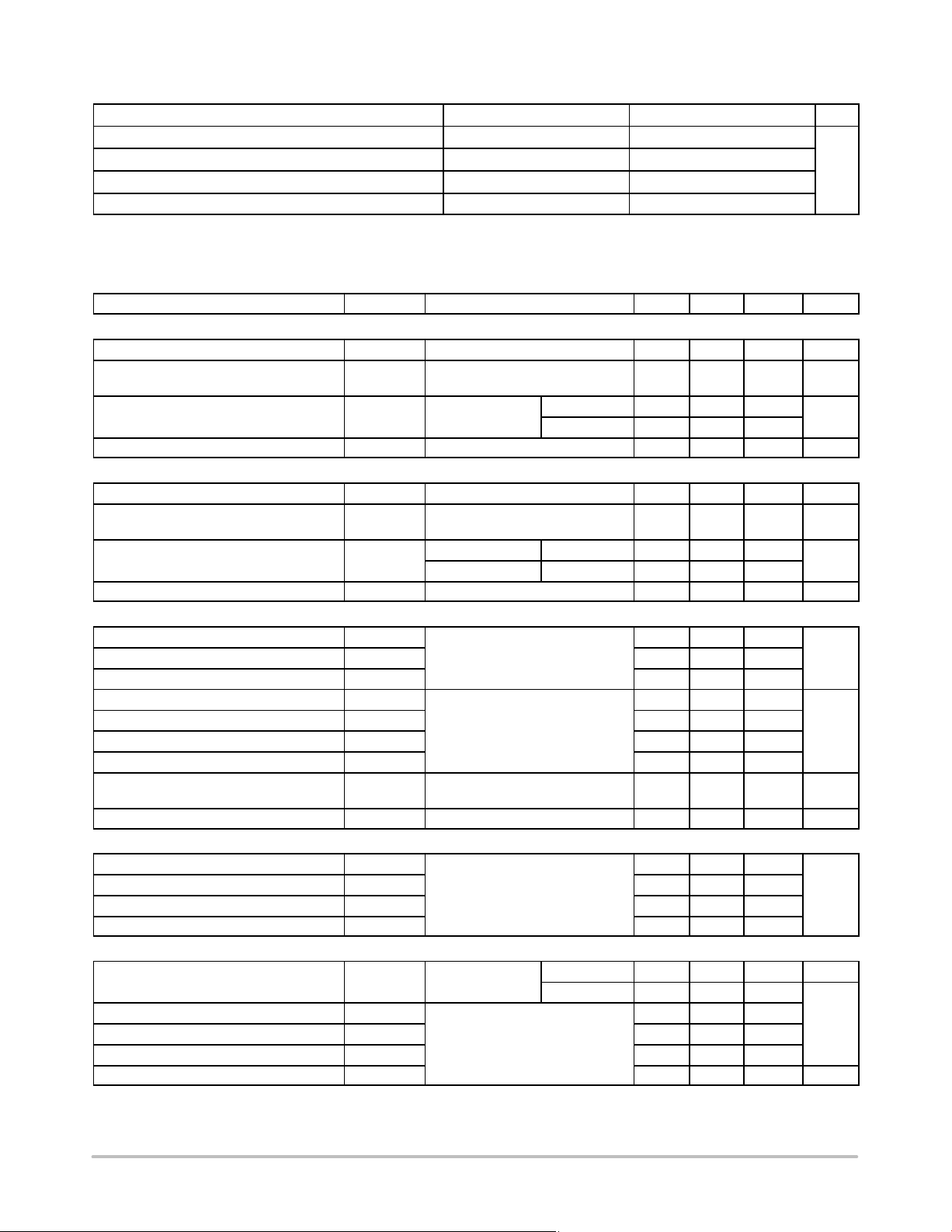
TYPICAL PERFORMANCE CURVES
20
18
16
14
12
10
-4.2 V
-4 V
-3.8 V
-10V
-5 V
-4.5 V
8
6
DRAIN CURRENT (AMPS)
4
D,
-I
2
0
0 0.5 1.0 1.5 2.0 2.5 3.0
-V
, DRAIN-TO-SOURCE VOLTAGE (VOLTS)
DS
Figure 1. On-Region Characteristics Figure 2. Transfer Characteristics
0.13
0.11
0.09
0.07
TJ = 25°C
-3.6 V
-3.4 V
-3.2 V
-3.0 V
-2.8 V
3.5 4.0 4.5 5.0
TJ = 25°C
I
= -9.6 A
D
20
VDS ≥ 10 V
18
16
14
12
10
8
6
DRAIN CURRENT (AMPS)
4
D,
-I
2
0
1.5 2.5 3.5 4.5
TJ = 125°C
TJ = 25°C
TJ = -55°C
-VGS, GATE-TO-SOURCE VOLTAGE (VOLTS)
0.030
TJ = 25°C
0.025
VGS = -4.5 V
0.020
0.05
0.03
DRAIN-TO-SOURCE RESISTANCE (W)
0.01
246 810
DS(on),
R
-VGS, GATE-TO-SOURCE VOLTAGE (VOLTS)
Figure 3. On-Resistance vs. Gate-to-Source
Voltage
1.6
ID = -9.6 A
V
= -10 V
GS
1.4
1.2
1.0
DRAIN-TO-SOURCE
0.8
DS(on),
R
RESISTANCE (NORMALIZED)
0.6
-50 -25 0 25 50 75 100 125 150
TJ, JUNCTION TEMPERATURE (°C)
0.015
DRAIN-TO-SOURCE RESISTANCE (W)
0.010
2101218
DS(on),
R
-I
VGS = -10 V
DRAIN CURRENT (AMPS)
D,
14 16468
Figure 4. On-Resistance vs. Drain Current and
Gate Voltage
10000
VGS = 0 V
TJ = 150°C
1000
, LEAKAGE (nA)
DSS
-I
100
51015202530
-VDS, DRAIN-TO-SOURCE VOLTAGE (VOLTS)
TJ = 125°C
Figure 5. On-Resistance Variation with
Temperature
http://onsemi.com
Figure 6. Drain-to-Source Leakage Current
vs. Voltage
3
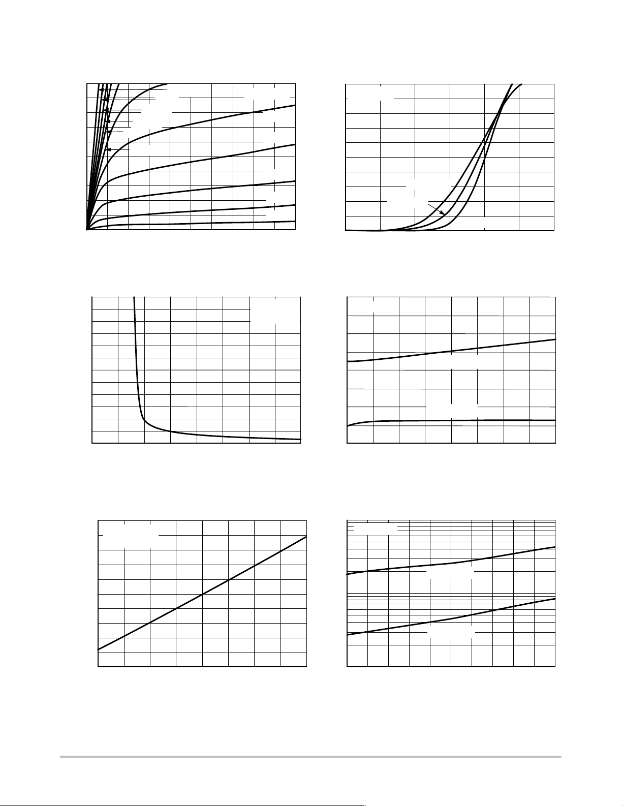
Page 4
2600
2200
C
iss
1800
1400
1000
C
C, CAPACITANCE (pF)
oss
600
C
rss
200
0510
DRAIN-TO-SOURCE VOLTAGE (VOLTS)
Figure 7. Capacitance Variation Figure 8. Gate-To-Source and
TYPICAL PERFORMANCE CURVES
TJ = 25°C
VGS = 0 V
15 25
20
NTMS4176P
10
9
8
7
6
5
Q
4
3
2
, GATE-TO-SOURCE VOLTAGE (VOLTS)
1
GS
0
-V
30
05
Drain-To-Source Voltage vs. Total Charge
QT
V
DS
Q
10
GD
15
GS
QG, TOTAL GATE CHARGE (nC)
V
GS
ID = -9.6 A
T
= 25°C
J
25 35
20 30
20
18
16
14
12
10
8
6
4
2
0
DS
-V
, DRAIN-TO-SOURCE VOLTAGE (VOLTS)
1000
VDD = -15 V
I
= -1 A
D
= -10 V
V
GS
100
t, TIME (ns)
10
1
1 10 100
RG, GATE RESISTANCE (OHMS)
Figure 9. Resistive Switching Time
Variation vs. Gate Resistance
100
10
1
VGS = -20 V
SINGLE PULSE
TC = 25°C
0.1
, DRAIN CURRENT (AMPS)
D
-I
0.01
0.1 10 100
R
LIMIT
DS(on)
THERMAL LIMIT
PACKAGE LIMIT
1
-VDS, DRAIN-TO-SOURCE VOLTAGE (VOLTS)
Figure 11. Maximum Rated Forward Biased
Safe Operating Area
t
d(off)
t
t
r
t
d(on)
10 ms
100 ms
1 ms
10 ms
dc
4
VGS = 0 V
T
= 25°C
J
f
3
2
1
, SOURCE CURRENT (AMPS)
S
-I
0
0.8
0.90.5 0.6 0.7
-VSD, SOURCE-TO-DRAIN VOLTAGE (VOLTS)
Figure 10. Diode Forward Voltage vs. Current
112.5
100
ID = -15 A
87.5
75
62.5
50
37.5
25
AVALANCHE ENERGY (mJ)
12.5
0
25 50 75 100
EAS, SINGLE PULSE DRAIN-TO-SOURCE
T
, STARTING JUNCTION TEMPERATURE (°C)
J
150125
Figure 12. Maximum Avalanche Energy vs.
Starting Junction Temperature
http://onsemi.com
4
Page 5
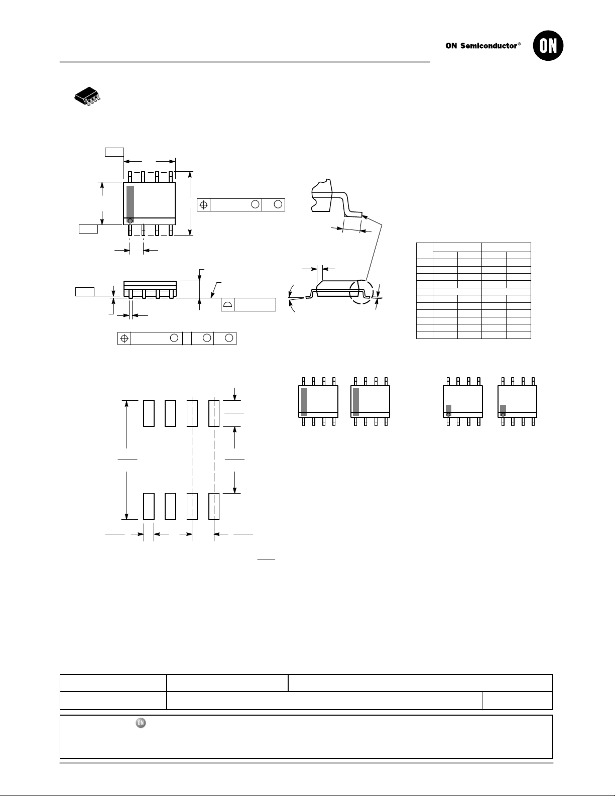
MECHANICAL CASE OUTLINE
PACKAGE DIMENSIONS
8
1
SCALE 1:1
B
−Y−
−Z−
H
−X−
A
58
S
1
4
G
D
0.25 (0.010) Z
M
SOLDERING FOOTPRINT*
7.0
0.275
Y
0.25 (0.010)
C
SEATING
PLANE
SXS
0.10 (0.004)
1.52
0.060
4.0
0.155
CASE 751−07
M
M
Y
N
SOIC−8 NB
ISSUE AK
K
X 45
_
M
J
MARKING DIAGRAM*
8
XXXXX
ALYWX
1
XXXXX = Specific Device Code
A = Assembly Location
L = Wafer Lot
Y = Year
W = Work Week
G = Pb−Free Package
8
XXXXX
ALYWX
G
1
IC
IC
(Pb−Free)
DATE 16 FEB 2011
NOTES:
1. DIMENSIONING AND TOLERANCING PER
ANSI Y14.5M, 1982.
2. CONTROLLING DIMENSION: MILLIMETER.
3. DIMENSION A AND B DO NOT INCLUDE
MOLD PROTRUSION.
4. MAXIMUM MOLD PROTRUSION 0.15 (0.006)
PER SIDE.
5. DIMENSION D DOES NOT INCLUDE DAMBAR
PROTRUSION. ALLOWABLE DAMBAR
PROTRUSION SHALL BE 0.127 (0.005) TOTAL
IN EXCESS OF THE D DIMENSION AT
MAXIMUM MATERIAL CONDITION.
6. 751−01 THRU 751−06 ARE OBSOLETE. NEW
STANDARD IS 751−07.
MILLIMETERS
DIMAMIN MAX MIN MAX
4.80 5.00 0.189 0.197
B 3.80 4.00 0.150 0.157
C 1.35 1.75 0.053 0.069
D 0.33 0.51 0.013 0.020
G 1.27 BSC 0.050 BSC
H 0.10 0.25 0.004 0.010
J 0.19 0.25 0.007 0.010
K 0.40 1.27 0.016 0.050
M 0 8 0 8
____
N 0.25 0.50 0.010 0.020
S 5.80 6.20 0.228 0.244
INCHES
GENERIC
8
XXXXXX
AYWW
1
Discrete
XXXXXX = Specific Device Code
A = Assembly Location
Y = Year
WW = Work Week
G = Pb−Free Package
8
XXXXXX
AYWW
1
Discrete
(Pb−Free)
G
0.6
0.024
1.270
0.050
SCALE 6:1
mm
ǒ
inches
Ǔ
*This information is generic. Please refer to
device data sheet for actual part marking.
Pb−Free indicator, “G” or microdot “G”, may
or may not be present. Some products may
not follow the Generic Marking.
*For additional information on our Pb−Free strategy and soldering
details, please download the ON Semiconductor Soldering and
Mounting Techniques Reference Manual, SOLDERRM/D.
STYLES ON PAGE 2
DOCUMENT NUMBER:
DESCRIPTION:
ON Semiconductor and are trademarks of Semiconductor Components Industries, LLC dba ON Semiconductor or its subsidiaries in the United States and/or other countries.
ON Semiconductor reserves the right to make changes without further notice to any products herein. ON Semiconductor makes no warranty, representation or guarantee regarding
the suitability of its products for any particular purpose, nor does ON Semiconductor assume any liability arising out of the application or use of any product or circuit, and specifically
disclaims any and all liability, including without limitation special, consequential or incidental damages. ON Semiconductor does not convey any license under its patent rights nor the
rights of others.
© Semiconductor Components Industries, LLC, 2019
98ASB42564B
SOIC−8 NB
Electronic versions are uncontrolled except when accessed directly from the Document Repository.
Printed versions are uncontrolled except when stamped “CONTROLLED COPY” in red.
PAGE 1 OF 2
www.onsemi.com
Page 6

STYLE 1:
PIN 1. EMITTER
2. COLLECTOR
3. COLLECTOR
4. EMITTER
5. EMITTER
6. BASE
7. BASE
8. EMITTER
STYLE 5:
PIN 1. DRAIN
2. DRAIN
3. DRAIN
4. DRAIN
5. GATE
6. GATE
7. SOURCE
8. SOURCE
STYLE 9:
PIN 1. EMITTER, COMMON
2. COLLECTOR, DIE #1
3. COLLECTOR, DIE #2
4. EMITTER, COMMON
5. EMITTER, COMMON
6. BASE, DIE #2
7. BASE, DIE #1
8. EMITTER, COMMON
STYLE 13:
PIN 1. N.C.
2. SOURCE
3. SOURCE
4. GATE
5. DRAIN
6. DRAIN
7. DRAIN
8. DRAIN
STYLE 17:
PIN 1. VCC
2. V2OUT
3. V1OUT
4. TXE
5. RXE
6. VEE
7. GND
8. ACC
STYLE 21:
PIN 1. CATHODE 1
2. CATHODE 2
3. CATHODE 3
4. CATHODE 4
5. CATHODE 5
6. COMMON ANODE
7. COMMON ANODE
8. CATHODE 6
STYLE 25:
PIN 1. VIN
2. N/C
3. REXT
4. GND
5. IOUT
6. IOUT
7. IOUT
8. IOUT
STYLE 29:
PIN 1. BASE, DIE #1
2. EMITTER, #1
3. BASE, #2
4. EMITTER, #2
5. COLLECTOR, #2
6. COLLECTOR, #2
7. COLLECTOR, #1
8. COLLECTOR, #1
STYLE 2:
PIN 1. COLLECTOR, DIE, #1
2. COLLECTOR, #1
3. COLLECTOR, #2
4. COLLECTOR, #2
5. BASE, #2
6. EMITTER, #2
7. BASE, #1
8. EMITTER, #1
STYLE 6:
PIN 1. SOURCE
2. DRAIN
3. DRAIN
4. SOURCE
5. SOURCE
6. GATE
7. GATE
8. SOURCE
STYLE 10:
PIN 1. GROUND
2. BIAS 1
3. OUTPUT
4. GROUND
5. GROUND
6. BIAS 2
7. INPUT
8. GROUND
STYLE 14:
PIN 1. N−SOURCE
2. N−GATE
3. P−SOURCE
4. P−GATE
5. P−DRAIN
6. P−DRAIN
7. N−DRAIN
8. N−DRAIN
STYLE 18:
PIN 1. ANODE
2. ANODE
3. SOURCE
4. GATE
5. DRAIN
6. DRAIN
7. CATHODE
8. CATHODE
STYLE 22:
PIN 1. I/O LINE 1
2. COMMON CATHODE/VCC
3. COMMON CATHODE/VCC
4. I/O LINE 3
5. COMMON ANODE/GND
6. I/O LINE 4
7. I/O LINE 5
8. COMMON ANODE/GND
STYLE 26:
PIN 1. GND
2. dv/dt
3. ENABLE
4. ILIMIT
5. SOURCE
6. SOURCE
7. SOURCE
8. VCC
STYLE 30:
PIN 1. DRAIN 1
2. DRAIN 1
3. GATE 2
4. SOURCE 2
5. SOURCE 1/DRAIN 2
6. SOURCE 1/DRAIN 2
7. SOURCE 1/DRAIN 2
8. GATE 1
SOIC−8 NB
CASE 751−07
ISSUE AK
STYLE 3:
STYLE 7:
STYLE 11:
STYLE 15:
PIN 1. DRAIN, DIE #1
2. DRAIN, #1
3. DRAIN, #2
4. DRAIN, #2
5. GATE, #2
6. SOURCE, #2
7. GATE, #1
8. SOURCE, #1
PIN 1. INPUT
2. EXTERNAL BYPASS
3. THIRD STAGE SOURCE
4. GROUND
5. DRAIN
6. GATE 3
7. SECOND STAGE Vd
8. FIRST STAGE Vd
PIN 1. SOURCE 1
2. GATE 1
3. SOURCE 2
4. GATE 2
5. DRAIN 2
6. DRAIN 2
7. DRAIN 1
8. DRAIN 1
PIN 1. ANODE 1
2. ANODE 1
3. ANODE 1
4. ANODE 1
5. CATHODE, COMMON
6. CATHODE, COMMON
7. CATHODE, COMMON
8. CATHODE, COMMON
STYLE 19:
PIN 1. SOURCE 1
2. GATE 1
3. SOURCE 2
4. GATE 2
5. DRAIN 2
6. MIRROR 2
7. DRAIN 1
8. MIRROR 1
STYLE 23:
PIN 1. LINE 1 IN
2. COMMON ANODE/GND
3. COMMON ANODE/GND
4. LINE 2 IN
5. LINE 2 OUT
6. COMMON ANODE/GND
7. COMMON ANODE/GND
8. LINE 1 OUT
STYLE 27:
PIN 1. ILIMIT
2. OVLO
3. UVLO
4. INPUT+
5. SOURCE
6. SOURCE
7. SOURCE
8. DRAIN
DATE 16 FEB 2011
STYLE 4:
PIN 1. ANODE
2. ANODE
3. ANODE
4. ANODE
5. ANODE
6. ANODE
7. ANODE
8. COMMON CATHODE
STYLE 8:
PIN 1. COLLECTOR, DIE #1
2. BASE, #1
3. BASE, #2
4. COLLECTOR, #2
5. COLLECTOR, #2
6. EMITTER, #2
7. EMITTER, #1
8. COLLECTOR, #1
STYLE 12:
PIN 1. SOURCE
2. SOURCE
3. SOURCE
4. GATE
5. DRAIN
6. DRAIN
7. DRAIN
8. DRAIN
STYLE 16:
PIN 1. EMITTER, DIE #1
2. BASE, DIE #1
3. EMITTER, DIE #2
4. BASE, DIE #2
5. COLLECTOR, DIE #2
6. COLLECTOR, DIE #2
7. COLLECTOR, DIE #1
8. COLLECTOR, DIE #1
STYLE 20:
PIN 1. SOURCE (N)
2. GATE (N)
3. SOURCE (P)
4. GATE (P)
5. DRAIN
6. DRAIN
7. DRAIN
8. DRAIN
STYLE 24:
PIN 1. BASE
2. EMITTER
3. COLLECTOR/ANODE
4. COLLECTOR/ANODE
5. CATHODE
6. CATHODE
7. COLLECTOR/ANODE
8. COLLECTOR/ANODE
STYLE 28:
PIN 1. SW_TO_GND
2. DASIC_OFF
3. DASIC_SW_DET
4. GND
5. V_MON
6. VBULK
7. VBULK
8. VIN
DOCUMENT NUMBER:
DESCRIPTION:
ON Semiconductor and are trademarks of Semiconductor Components Industries, LLC dba ON Semiconductor or its subsidiaries in the United States and/or other countries.
ON Semiconductor reserves the right to make changes without further notice to any products herein. ON Semiconductor makes no warranty, representation or guarantee regarding
the suitability of its products for any particular purpose, nor does ON Semiconductor assume any liability arising out of the application or use of any product or circuit, and specifically
disclaims any and all liability, including without limitation special, consequential or incidental damages. ON Semiconductor does not convey any license under its patent rights nor the
rights of others.
© Semiconductor Components Industries, LLC, 2019
98ASB42564B
SOIC−8 NB
Electronic versions are uncontrolled except when accessed directly from the Document Repository.
Printed versions are uncontrolled except when stamped “CONTROLLED COPY” in red.
PAGE 2 OF 2
www.onsemi.com
Page 7
ON Semiconductor and are trademarks of Semiconductor Components Industries, LLC dba ON Semiconductor or its subsidiaries in the United States and/or other countries.
ON Semiconductor owns the rights to a number of patents, trademarks, copyrights, trade secrets, and other intellectual property. A listing of ON Semiconductor ’s product/patent
coverage may be accessed at www.onsemi.com/site/pdf/Patent−Marking.pdf
ON Semiconductor makes no warranty, representation or guarantee regarding the suitability of its products for any particular purpose, nor does ON Semiconductor assume any liability
arising out of the application or use of any product or circuit, and specifically disclaims any and all liability, including without limitation special, consequential or incidental damages.
Buyer is responsible for its products and applications using ON Semiconductor products, including compliance with all laws, regulations and safety requirements or standards,
regardless of any support or applications information provided by ON Semiconductor. “Typical” parameters which may be provided in ON Semiconductor data sheets and/or
specifications can and do vary in different applications and actual performance may vary over time. All operating parameters, including “Typicals” must be validated for each customer
application by customer’s technical experts. ON Semiconductor does not convey any license under its patent rights nor the rights of others. ON Semiconductor products are not
designed, intended, or authorized for use as a critical component in life support systems or any FDA Class 3 medical devices or medical devices with a same or similar classification
in a foreign jurisdiction or any devices intended for implantation in the human body. Should Buyer purchase or use ON Semiconductor products for any such unintended or unauthorized
application, Buyer shall indemnify and hold ON Semiconductor and its officers, employees, subsidiaries, affiliates, and distributors harmless against all claims, costs, damages, and
expenses, and reasonable attorney fees arising out of, directly or indirectly, any claim of personal injury or death associated with such unintended or unauthorized use, even if such
claim alleges that ON Semiconductor was negligent regarding the design or manufacture of the part. ON Semiconductor is an Equal Opportunity/Affirmative Action Employer. This
literature is subject to all applicable copyright laws and is not for resale in any manner.
. ON Semiconductor reserves the right to make changes without further notice to any products herein.
PUBLICATION ORDERING INFORMATION
LITERATURE FULFILLMENT:
Email Requests to: orderlit@onsemi.com
ON Semiconductor Website: www.onsemi.com
TECHNICAL SUPPORT
North American Technical Support:
Voice Mail: 1 800−282−9855 Toll Free USA/Canada
Phone: 011 421 33 790 2910
Europe, Middle East and Africa Technical Support:
Phone: 00421 33 790 2910
For additional information, please contact your local Sales Representative
◊
www.onsemi.com
1
 Loading...