

Page 1
NTK3043N
MOSFET – Power,
N-Channel with ESD
Protection, SOT-723
20 V, 285 mA
Features
• Enables High Density PCB Manufacturing
• 44% Smaller Footprint than SC−89 and 38% Thinner than SC−89
• Low Voltage Drive Makes this Device Ideal for Portable Equipment
• Low Threshold Levels, V
• Low Profile (< 0.5 mm) Allows It to Fit Easily into Extremely Thin
Environments such as Portable Electronics
• Operated at Standard Logic Level Gate Drive, Facilitating Future
Migration to Lower Levels Using the Same Basic Topology
• These are Pb−Free and Halogen−Free Devices
Applications
• Interfacing, Switching
• High Speed Switching
• Cellular Phones, PDAs
GS(TH)
< 1.3 V
V
(BR)DSS
20 V
www.onsemi.com
R
TYP ID Max
DS(on)
1.5 W @ 4.5 V
2.4 W @ 2.5 V
5.1 W @ 1.8 V
6.8 W @ 1.65 V
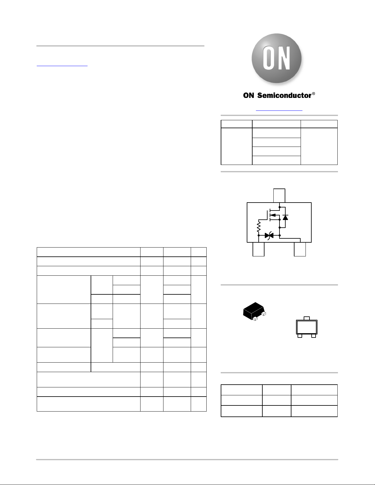
Top View
3
285 mA
MAXIMUM RATINGS (T
Parameter
Drain−to−Source Voltage V
Gate−to−Source Voltage V
Continuous Drain
Current (Note 1)
Power Dissipation
(Note 1)
Continuous Drain
Current (Note 2)
Power Dissipation
(Note 2)
Pulsed Drain Current
Operating Junction and Storage Temperature TJ, T
Source Current (Body Diode) (Note 2) I
Lead Temperature for Soldering Purposes
(1/8” from case for 10 seconds)
Stresses exceeding those listed in the Maximum Ratings table may damage the
device. If any of these limits are exceeded, device functionality should not be
assumed, damage may occur and reliability may be affected.
1. Surface−mounted on FR4 board using 1 in sq pad size
(Cu area = 1.127 in sq [1 oz] including traces)
2. Surface−mounted on FR4 board using the minimum recommended pad size.
= 25°C unless otherwise stated)
J
Symbol Value Unit
DSS
GS
Steady
State
t v 5 s TA = 25°C 285
Steady
State
t v 5 s 545
Steady
State
TA = 25°C
TA = 85°C 185
TA = 25°C P
TA = 25°C
TA = 85°C 155
TA = 25°C P
tp = 10 ms
I
D
D
I
D
D
I
DM
STG
S
T
L
20 V
±10 V
255
440
210
310
400 mA
−55 to
150
286 mA
260 °C
mA
mW
mA
mW
°C
12
1 − Gate
2 − Source
3 − Drain
MARKING
DIAGRAM
KA
SOT−723
CASE 631AA
STYLE 5
KA = Device Code
M = Date Code
1
M
ORDERING INFORMATION
Device Package Shipping
NTK3043NT1G SOT−723* 4000 / Tape & Reel
NTK3043NT5G SOT−723* 8000 / Tape & Reel
†For information on tape and reel specifications,
including part orientation and tape sizes, please
refer to our Tape and Reel Packaging Specification
Brochure, BRD8011/D.
*These packages are inherently Pb−Free.
†
© Semiconductor Components Industries, LLC, 2013
July, 2019 − Rev. 5
1 Publication Order Number:
NTK3043N/D
Page 2
NTK3043N
THERMAL RESISTANCE RATINGS
Parameter Symbol Max Unit
Junction−to−Ambient – Steady State (Note 3)
Junction−to−Ambient – t = 5 s (Note 3)
Junction−to−Ambient – Steady State Minimum Pad (Note 4)
3. Surface−mounted on FR4 board using 1 in sq pad size (Cu area = 1.127 in sq [1 oz] including traces)
4. Surface−mounted on FR4 board using the minimum recommended pad size.
R
q
JA
R
q
JA
R
q
JA
280
228
400
°C/W
ELECTRICAL CHARACTERISTICS (T
Parameter
= 25°C unless otherwise specified)
J
Test Condition Symbol Min Typ Max Unit
OFF CHARACTERISTICS
Drain−to−Source Breakdown Voltage
Drain−to−Source Breakdown Voltage
VGS = 0 V, ID = 100 mA
ID = 100 mA, Reference to 25°C
V
Temperature Coefficient
Zero Gate Voltage Drain Current VGS = 0 V,
V
= 16 V
DS
TJ = 25°C
TJ = 125°C 10
Gate−to−Source Leakage Current VDS = 0 V, VGS = ±5 V I
ON CHARACTERISTICS (Note 3)
Gate Threshold Voltage
Gate Threshold Temperature Coefficient V
Drain−to−Source On Resistance
VGS = VDS, ID = 250 mA
VGS = 4.5V, ID = 10 mA
VGS = 4.5V, ID = 255 mA 1.6 3.8
VGS = 2.5 V, ID = 1 mA 2.4 4.5
VGS = 1.8 V, ID = 1 mA 5.1 10
VGS = 1.65 V, ID = 1 mA 6.8 15
Forward Transconductance VDS = 5 V, ID = 100 mA g
Gate Resistance TA = 25°C R
CHARGES, CAPACITANCES AND GATE RESISTANCE
Input Capacitance
Output Capacitance C
VGS = 0 V, f = 1 MHz, VDS = 10 V
Reverse Transfer Capacitance C
SWITCHING CHARACTERISTICS, VGS= 4.5 V (Note 4)
Turn−On Delay Time
Rise Time t
Turn−Off Delay Time t
VGS = 4.5 V, VDD = 5 V, ID = 10 mA,
= 6 W
R
G
Fall Time t
DRAIN−SOURCE DIODE CHARACTERISTICS
Forward Diode Voltage
VGS = 0 V, IS= 286 mA
TJ = 25°C
TJ = 125°C 0.69
Reverse Recovery Time
Charge Time t
Discharge Time t
VGS = 0 V, VDD = 20 V, dISD/dt = 100 A/ms,
I
= 286 mA
S
Reverse Recovery Charge Q
5. Pulse Test: pulse width v 300 ms, duty cycle v 2%
6. Switching characteristics are independent of operating junction temperatures
V
(BR)DSS
(BR)DSS/TJ
I
DSS
GSS
V
GS(TH)
GS(TH)/TJ
R
DS(ON)
FS
G
C
ISS
OSS
RSS
t
d(ON)
r
d(OFF)
f
V
SD
t
RR
a
b
RR
20 V
27
mV/°C
1
1
0.4 1.3 V
−2.4 mV/°C
1.5 3.4
0.275 S
2.2
11
8.3
2.7
13
15
94
55
0.83 1.2
9.1
7.1
2.0
3.7 nC
mA
mA
W
kW
pF
ns
V
ns
www.onsemi.com
2
Page 3

NTK3043N
TYPICAL PERFORMANCE CURVES
0.3
VGS = 3 V to 10 V
0.2
0.1
DRAIN CURRENT (AMPS)
D,
I
0
0
1
V
, DRAIN−TO−SOURCE VOLTAGE (VOLTS)
DS
Figure 1. On−Region Characteristics
5
4
3
2
0.3
2.5 V
VDS ≥ 5 V
TJ = 25°C
2.2 V
0.2
2.0 V
0.1
1.8 V
1.6 V
1.4 V
2
35
4
DRAIN CURRENT (AMPS)
D,
I
TJ = 25°C
0
12
TJ = 125°C
1.5
TJ = −55°C
2.5
VGS, GATE−TO−SOURCE VOLTAGE (VOLTS)
Figure 2. Transfer Characteristics
ID = 0.255 A
= 25°C
T
J
6
TJ = 25°C
5
4
VGS = 2.5 V
3
1
DRAIN−TO−SOURCE RESISTANCE (W)
2
DRAIN−TO−SOURCE RESISTANCE (W)
VGS = 4.5 V
01
16
DS(on),
R
27593
V
, GATE−TO−SOURCE VOLTAGE (VOLTS)
GS
4
8 0.2
Figure 3. On−Resistance vs. Gate−to−Source
Voltage
9.0
8.0
7.0
6.0
VGS = 1.8 V, ID = 10 mA
VGS = 1.65 V, ID = 1 mA
10
0 0.30.1
DS(on),
R
ID, DRAIN CURRENT (AMPS)
Figure 4. On−Resistance vs. Drain Current and
Gate Voltage
1000
100
VGS = 0 V
TJ = 150°C
5.0
4.0
DRAIN−TO−SOURCE
RESISTANCE
3.0
2.0
DS(on),
R
1.0
0
−50 0−25 25
Figure 5. On−Resistance Variation with
VGS = 2.5 V, ID = 10 mA
VGS = 4.5 V, ID = 10 mA
75
50 150
TJ, JUNCTION TEMPERATURE (°C)
Temperature
10
, LEAKAGE (nA)
DSS
I
1
125100
5
VDS, DRAIN−TO−SOURCE VOLTAGE (VOLTS)
Figure 6. Drain−to−Source Leakage Current
TJ = 125°C
10
vs. Voltage
15
20
www.onsemi.com
3
Page 4

NTK3043N
TYPICAL PERFORMANCE CURVES
25
TJ = 25°C
20
C
iss
C
rss
15
10
C, CAPACITANCE (pF)
5
0
VGS = 0 VVDS = 0 V
10 5 0 5 10 15 20
GS
V
DS
V
GATE−TO−SOURCE OR DRAIN−TO−SOURCE VOLTAGE (V)
Figure 7. Capacitance Variation
1000
VDD = 5 V
= 10 mA
I
D
V
= 4.5 V
GS
100
t
d(off)
t
f
C
iss
C
oss
C
rss
t
t, TIME (ns)
10
1
r
t
d(on)
1 10 100
, GATE RESISTANCE (OHMS)
R
G
Figure 8. Resistive Switching Time
Variation vs. Gate Resistance
0.4
VGS = 0 V
TJ = 25°C
0.3
0.2
0.1
, SOURCE CURRENT (AMPS)
S
I
TJ = 150°C
TJ = 125°C
0
0.4 0.70.5
, SOURCE−TO−DRAIN VOLTAGE (VOLTS)
V
SD
Figure 9. Diode Forward Voltage vs. Current
TJ = −55°C
0.90.8
1.00.6
www.onsemi.com
4
Page 5

MECHANICAL CASE OUTLINE
PACKAGE DIMENSIONS
SCALE 4:1
−X−
D
2X
b1
3
1
e
TOP VIEW
1
−Y−
E
2
b
2X
X0.08 Y
3X
L
SOT−723
CASE 631AA−01
ISSUE D
A
H
E
C
SIDE VIEW
DATE 10 AUG 2009
NOTES:
1. DIMENSIONING AND TOLERANCING PER ASME
Y14.5M, 1994.
2. CONTROLLING DIMENSION: MILLIMETERS.
3. MAXIMUM LEAD THICKNESS INCLUDES LEAD
FINISH. MINIMUM LEAD THICKNESS IS THE MINIMUM
THICKNESS OF BASE MATERIAL.
4. DIMENSIONS D AND E DO NOT INCLUDE MOLD
FLASH, PROTRUSIONS OR GATE BURRS.
MILLIMETERS
DIM MIN NOM MAX
A 0.45 0.50 0.55
b 0.15 0.21 0.27
b1 0.25 0.31 0.37
C 0.07 0.12 0.17
D 1.15 1.20 1.25
E 0.75 0.80 0.85
e
H 1.15 1.20 1.25
L
L2 0.15 0.20 0.25
0.40 BSC
E
0.29 REF
3X
L2
BOTTOM VIEW
STYLE 1:
PIN 1. BASE
2. EMITTER
3. COLLECTOR
STYLE 2:
PIN 1. ANODE
2. N/C
3. CATHODE
STYLE 3:
PIN 1. ANODE
2. ANODE
3. CATHODE
STYLE 4:
RECOMMENDED
SOLDERING FOOTPRINT*
2X
0.40
2X
0.27
PACKAGE
OUTLINE
1.50
3X
0.52
*For additional information on our Pb−Free strategy and soldering
details, please download the ON Semiconductor Soldering and
Mounting Techniques Reference Manual, SOLDERRM/D.
0.36
DIMENSIONS: MILLIMETERS
PIN 1. CATHODE
2. CATHODE
3. ANODE
STYLE 5:
PIN 1. GATE
2. SOURCE
3. DRAIN
GENERIC
MARKING DIAGRAM*
XX M
1
XX = Specific Device Code
M = Date Code
*This information is generic. Please refer
to device data sheet for actual part
marking. Pb−Free indicator, “G”, may
or not be present.
DOCUMENT NUMBER:
DESCRIPTION:
ON Semiconductor and are trademarks of Semiconductor Components Industries, LLC dba ON Semiconductor or its subsidiaries in the United States and/or other countries.
ON Semiconductor reserves the right to make changes without further notice to any products herein. ON Semiconductor makes no warranty, representation or guarantee regarding
the suitability of its products for any particular purpose, nor does ON Semiconductor assume any liability arising out of the application or use of any product or circuit, and specifically
disclaims any and all liability, including without limitation special, consequential or incidental damages. ON Semiconductor does not convey any license under its patent rights nor the
rights of others.
© Semiconductor Components Industries, LLC, 2019
98AON12989D
SOT−723
Electronic versions are uncontrolled except when accessed directly from the Document Repository.
Printed versions are uncontrolled except when stamped “CONTROLLED COPY” in red.
PAGE 1 OF 1
www.onsemi.com
Page 6

ON Semiconductor and are trademarks of Semiconductor Components Industries, LLC dba ON Semiconductor or its subsidiaries in the United States and/or other countries.
ON Semiconductor owns the rights to a number of patents, trademarks, copyrights, trade secrets, and other intellectual property. A listing of ON Semiconductor’s product/patent
coverage may be accessed at www.onsemi.com/site/pdf/Patent−Marking.pdf
ON Semiconductor makes no warranty, representation or guarantee regarding the suitability of its products for any particular purpose, nor does ON Semiconductor assume any liability
arising out of the application or use of any product or circuit, and specifically disclaims any and all liability, including without limitation special, consequential or incidental damages.
Buyer is responsible for its products and applications using ON Semiconductor products, including compliance with all laws, regulations and safety requirements or standards,
regardless of any support or applications information provided by ON Semiconductor. “Typical” parameters which may be provided in ON Semiconductor data sheets and/or
specifications can and do vary in different applications and actual performance may vary over time. All operating parameters, including “Typicals” must be validated for each customer
application by customer’s technical experts. ON Semiconductor does not convey any license under its patent rights nor the rights of others. ON Semiconductor products are not
designed, intended, or authorized for use as a critical component in life support systems or any FDA Class 3 medical devices or medical devices with a same or similar classification
in a foreign jurisdiction or any devices intended for implantation in the human body. Should Buyer purchase or use ON Semiconductor products for any such unintended or unauthorized
application, Buyer shall indemnify and hold ON Semiconductor and its officers, employees, subsidiaries, affiliates, and distributors harmless against all claims, costs, damages, and
expenses, and reasonable attorney fees arising out of, directly or indirectly, any claim of personal injury or death associated with such unintended or unauthorized use, even if such
claim alleges that ON Semiconductor was negligent regarding the design or manufacture of the part. ON Semiconductor is an Equal Opportunity/Affirmative Action Employer. This
literature is subject to all applicable copyright laws and is not for resale in any manner.
. ON Semiconductor reserves the right to make changes without further notice to any products herein.
PUBLICATION ORDERING INFORMATION
LITERATURE FULFILLMENT:
Email Requests to: orderlit@onsemi.com
ON Semiconductor Website: www.onsemi.com
TECHNICAL SUPPORT
North American Technical Support:
Voice Mail: 1 800−282−9855 Toll Free USA/Canada
Phone: 011 421 33 790 2910
Europe, Middle East and Africa Technical Support:
Phone: 00421 33 790 2910
For additional information, please contact your local Sales Representative
◊
www.onsemi.com
1
 Loading...