

Page 1
NTJD1155L
MOSFET – Power,
P-Channel, High Side Load
Switch with Level-Shift,
SC-88
8 V, +1.3 A
www.onsemi.com
The NTJD1155L integrates a P and N−Channel MOSFET in a single
package. This device is particularly suited for portable electronic
equipment where low control signals, low battery voltages and high
load currents are needed. The P−Channel device is specifically
designed as a load switch using ON Semiconductor state−of−the−art
trench technology. The N−Channel, with an external resistor (R1),
functions as a level−shift to drive the P−Channel. The N−Channel
MOSFET has internal ESD protection and can be driven by logic
signals as low as 1.5 V. The NTJD1155L operates on supply lines from
1.8 to 8.0 V and can drive loads up to 1.3 A with 8.0 V applied to both
V
and V
IN
ON/OFF.
Features
• Extremely Low R
P−Channel Load Switch MOSFET
DS(on)
• Level Shift MOSFET is ESD Protected
• Low Profile, Small Footprint Package
• V
Range 1.8 to 8.0 V
IN
• ON/OFF Range 1.5 to 8.0 V
• These Devices are Pb−Free and are RoHS Compliant
MAXIMUM RATINGS (T
Input Voltage (V
ON/OFF Voltage (VGS, N−Ch) V
Continuous Load Current
(Note 1)
Power Dissipation
(Note 1)
Pulsed Load Current
Operating Junction and Storage Temperature TJ,
Source Current (Body Diode) I
Lead Temperature for Soldering Purposes
(1/8″ from case for 10 s)
DSS
THERMAL CHARACTERISTICS
Characteristic Symbol Max Unit
Junction−to−Ambient – Steady State (Note 1)
Junction−to−Foot – Steady State (Note 1)
Stresses exceeding those listed in the Maximum Ratings table may damage the
device. If any of these limits are exceeded, device functionality should not be
assumed, damage may occur and reliability may be affected.
= 25°C unless otherwise noted)
J
Rating
, P−Ch) V
Steady
State
Steady
State
T
= 25°C
A
T
= 85°C ±0.9
A
T
= 25°C
A
T
= 85°C 0.20
A
t
= 10 ms
p
Symbol Value Unit
ON/OFF
T
R
R
IN
I
L
P
I
LM
STG
S
T
q
q
D
L
JA
JF
8.0 V
8.0 V
±1.3
0.40
±3.9 A
−55 to
150
−0.4 A
260 °C
320
220
A
W
°C
°C/W
(BR)DSS
8.0 V
TYP
DS(on)
130 mW @ −4.5 V
170 mW @ −2.5 V
260 mW @ −1.8 V
ID MAXV
±1.3 A
R
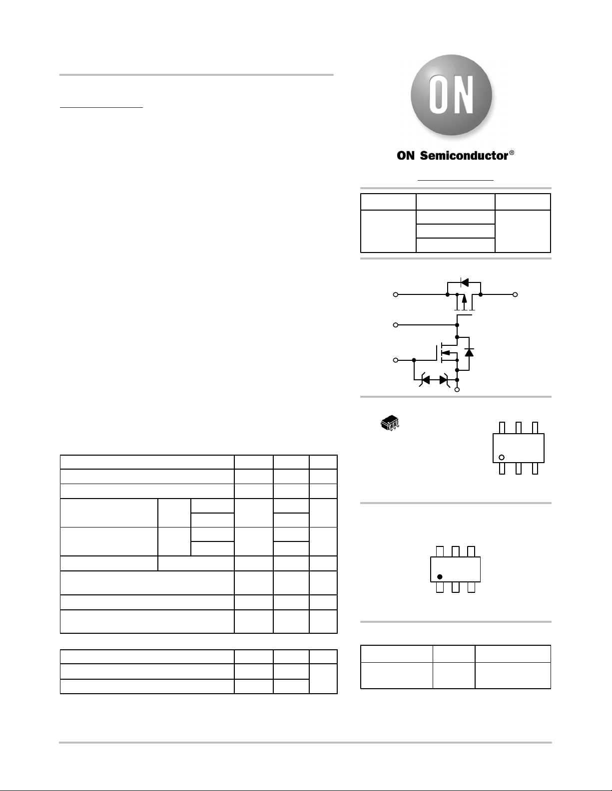
SIMPLIFIED SCHEMATIC
4
6
5
2,3
Q2
Q1
1
MARKING
SC−88
(SOT−363)
1
CASE 419B
STYLE 30
TB = Device Code
M = Date Code
G = Pb−Free Package
(Note: Microdot may be in either location)
DIAGRAM
TB M G
G
1
PIN ASSIGNMENT
S1
G1
S2
5
6
1
D2
4
2
3
D2
D1/G2
ORDERING INFORMATION
Device Package Shipping
NTJD1155LT1G,
NTJD1155LT2G
†For information on tape and reel specifications,
including part orientation and tape sizes, please
refer to our Tape and Reel Packaging Specification
Brochure, BRD8011/D.
SC−88
(Pb−Free)
3000/Tape & Reel
†
© Semiconductor Components Industries, LLC, 2012
May, 2019 − Rev. 6
1 Publication Order Number:
NTJD1155L/D
Page 2

1. Surface−mounted on FR4 board using 1 inch sq pad size
(Cu area = 1.127 in sq [1 oz] including traces).
NTJD1155L
www.onsemi.com
2
Page 3
NTJD1155L
ELECTRICAL CHARACTERISTICS (T
= 25°C unless otherwise noted)
J
Characteristic Symbol Test Condition Min Ty p Max Unit
OFF CHARACTERISTICS
Q2 Drain−to−Source Breakdown Voltage
Forward Leakage Current I
Q1 Gate−to−Source Leakage Current I
Q1 Diode Forward On−Voltage V
ON CHARACTERISTICS
ON/OFF Voltage
V
Q1 Gate Threshold Voltage V
Input Voltage V
Q2 Drain−to−Source On Resistance R
Load Current I
V
IN
FL
GSS
SD
ON/OFF
GS1(th)
IN
DS(on)
L
V
V
V
DS2
V
V
V
V
ON/OFF
V
V
= 0 V, I
GS2
= 0 V,
GS1
= −8.0 V
= 0 V, V
DS1
I
= −0.4 A, V
S
= V
GS1
= V
GS1
= 1.5 V
≤ 0.2 V, V
DROP
V
ON/OFF
≤ 0.3 V, V
DROP
V
ON/OFF
= 250 mA
D2
−8.0 V
TJ = 25°C 1.0 mA
TJ = 125°C 10
= ±8.0 V ±100 nA
GS1
= 0 V −0.8 −1.1 V
GS1
1.5 8.0 V
DS1
DS1
, I
= 250 mA
D
, I
= 250 mA
D
IN
= 1.5 V
IN
= 1.5 V
V
= 4.5 V
IN
I
= 1.2 A
L
V
= 2.5 V
IN
I
= 1.0 A
L
V
= 1.8 V
IN
I
= 0.7 A
L
= 5.0 V,
= 2.5 V,
0.4 1.0 V
1.8 8.0 V
130 175 mW
170 220
260 320
1.0
1.0
A
V
IN
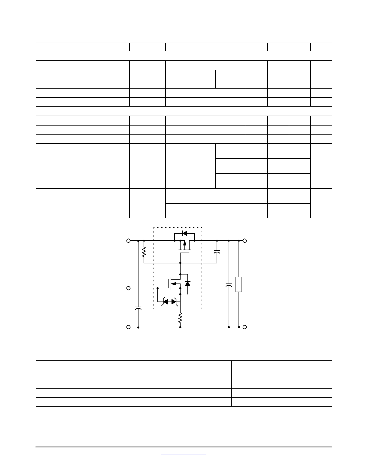
R1
4
Q2
6
ON/OFF
5
Q1
C
I
R2
Figure 1. Load Switch Application
Components Description Values
R1 Pullup Resistor
R2 Optional Slew−Rate Control
CO, C
I
C1 Optional In−Rush Current Control Typical ≤ 1000 pF
*Minimum R1 value should be at least 10 x R2 to ensure Q1 turn−on.
Output Capacitance
1
R2
2,3
V
OUT
C1
6
C
O
LOAD
GND
Typical 10 kW to 1.0 MW*
Typical 0 to 100 kW*
Usually < 1.0 mF
www.onsemi.com
3
Page 4

NTJD1155L
0.70
0.65
0.60
0.55
0.50
0.45
0.40
(V)
0.35
0.30
DROP
V
0.25
0.20
0.15
0.10
0.05
0.8
0.7
0.6
0.5
TYPICAL PERFORMANCE CURVES (T
= 25°C unless otherwise noted)
J
0.50
0.45
0.40
(V)
0.35
0.30
TJ = 125°C
TJ = 125°C
0.25
DROP
0.20
TJ = 25°C
V
TJ = 25°C
0.15
0.10
0.05
0
0
1.0
1.50.5
2.0
3.02.5
IL (AMPS)
Figure 2. V
vs. IL @ Vin = 2.5 V Figure 3. V
drop
0
0
1.0 3.02.5
1.50.5
2.0
IL (AMPS)
vs. IL @ Vin = 4.5 V
drop
0.31
IL = 1 A
V
ON/OFF
= 1.5 to 8 V
0.26
IL = 1 A
V
ON/OFF
= 1.5 to 8 V
Vin = 1.8 V
0.21
0.4
0.3
0.2
0.1
DRAIN−TO−SOURCE RESISTANCE (W)
0.0
2.0 4.0 6.0
1.0
DS(on),
R
Figure 4. On−Resistance vs. Input Voltage
1.7
IL = 1 A
V
ON/OFF
1.5
1.3
1.1
DRAIN−TO−SOURCE
0.9
DS(on),
R
RESISTANCE (NORMALIZED)
0.7
−50 0−25 25
Figure 6. Normalized On−Resistance Variation
TJ = 125°C
TJ = 25°C
3.0 5.0 7.0
VIN (VOLTS)
= 1.5 to 8 V
Vin = 5 V
Vin = 1.8 V
75 150
50 125100
TJ, JUNCTION TEMPERATURE (°C)
with Temperature
8.0
0.16
0.11
Vin = 5 V
0.06
DRAIN−TO−SOURCE RESISTANCE (W)
0.01
−50 0−25 25 50 12510075 150
DS(on),
R
T
, JUNCTION TEMPERATURE (°C)
J
Figure 5. On−Resistance Variation with
Temperature
44
IL = 1 A
40
36
32
V
ON/OFF
Ci = 10 mF
Co = 1 mF
= 1.5 V
t
r
28
24
20
TIME (ms)
16
t
d(off)
t
f
12
8
4
0
08
37
241
t
d(on)
56
R2 (kW)
Figure 7. Switching Variation
R2 @ V
= 4.5 V, R1 = 20 kW
in
www.onsemi.com
4
Page 5

NTJD1155L
TYPICAL PERFORMANCE CURVES (T
22
20
18
16
14
t
d(off)
t
f
12
10
TIME (ms)
IL = 1 A
= 3 V
V
8
on/off
Ci = 10 mF
6
Co = 1 mF
4
2
0
08
241
37
56
t
r
t
d(on)
R2 (kW)
Figure 8. Switching Variation
R2 @ V
= 4.5 V, R1 = 20 kW
in
= 25°C unless otherwise noted)
J
40
IL = 1 A
36
32
28
V
ON/OFF
Ci = 10 mF
Co = 1 mF
= 1.5 V
24
20
TIME (ms)
16
12
t
f
8
4
0
08
241
37
R2 (kW)
Figure 9. Switching Variation
R2 @ V
= 2.5 V, R1 = 20 kW
in
12
t
10
f
56
t
d(off)
t
d(on)
t
r
10
1
0.2
0.1
0.1
SINGLE PULSE
0.01
r(t), EFFECTIVE TRANSIENT THERMAL RESPONSE
D = 0.5
Normalized to R
0.02
0.01
8
IL = 1 A
= 3 V
V
on/off
6
TIME (ms)
Ci = 10 mF
Co = 1 mF
t
d(off)
t
r
4
2
t
d(on)
0
08
37
241
56
R2 (kW)
Figure 10. Switching Variation
R2 @ V
at Steady State ( 1 inch pad)
q
JA
0.05
SQUARE WAVE PULSE DURATION TIME t, (s)
= 2.5 V, R1 = 20 kW
in
P
(pk)
t
1
t
DUTY CYCLE, D = t1/t
R
(t) = r(t) R
q
JC
q
JC
D CURVES APPLY FOR POWER
PULSE TRAIN SHOWN
2
2
T
J(pk)
− TC = P
READ TIME AT t
(pk)
1
R
(t)
q
JC
100 10001010.10.010.001
Figure 11. FET Thermal Response
www.onsemi.com
5
Page 6

MECHANICAL CASE OUTLINE
PACKAGE DIMENSIONS
SC−88/SC70−6/SOT−363
1
SCALE 2:1
D
A
654
E
123
2X
bbb H
D
e
B
TOP VIEW
6X
ccc
C
SIDE VIEW END VIEW
RECOMMENDED
SOLDERING FOOTPRINT*
6X
0.30
0.65
PITCH
*For additional information on our Pb−Free strategy and soldering
details, please download the ON Semiconductor Soldering and
Mounting Techniques Reference Manual, SOLDERRM/D.
2X
aaa H D
D
E1
L2
aaa C
2X 3 TIPS
b
6X
M
A2
A
A1
C
6X
0.66
SEATING
PLANE
2.50
DIMENSIONS: MILLIMETERS
Cddd
A-B D
DETAIL A
CASE 419B−02
ISSUE Y
H
L
DETAIL A
GAGE
PLANE
DATE 11 DEC 2012
NOTES:
1. DIMENSIONING AND TOLERANCING PER ASME Y14.5M, 1994.
2. CONTROLLING DIMENSION: MILLIMETERS.
3. DIMENSIONS D AND E1 DO NOT INCLUDE MOLD FLASH,
PROTRUSIONS, OR GATE BURRS. MOLD FLASH, PROTRUSIONS, OR GATE BURRS SHALL NOT EXCEED 0.20 PER END.
4. DIMENSIONS D AND E1 AT THE OUTERMOST EXTREMES OF
THE PLASTIC BODY AND DATUM H.
5. DATUMS A AND B ARE DETERMINED AT DATUM H.
6. DIMENSIONS b AND c APPLY TO THE FLAT SECTION OF THE
LEAD BETWEEN 0.08 AND 0.15 FROM THE TIP.
7. DIMENSION b DOES NOT INCLUDE DAMBAR PROTRUSION.
ALLOWABLE DAMBAR PROTRUSION SHALL BE 0.08 TOTAL IN
EXCESS OF DIMENSION b AT MAXIMUM MATERIAL CONDITION. THE DAMBAR CANNOT BE LOCATED ON THE LOWER
RADIUS OF THE FOOT.
MILLIMETERS
DIM MIN NOM MAX
A −−− −−− 1.10
A1 0.00 −−− 0.10
A2 0.70 0.90 1.00 0.027 0.035 0.039
b 0.15 0.20 0.25
C 0.08 0.15 0.22
D 1.80 2.00 2.20
E
2.00 2.10 2.20
E1 1.15 1.25 1.35
e 0.65 BSC
L 0.26 0.36 0.46
L2 0.15 BSC 0.006 BSC
aaa 0.15 0.006
bbb 0.30 0.012
ccc 0.10 0.004
ddd
c
0.10 0.004
INCHES
MIN NOM MAX
−−− −−− 0.043
0.000 −−− 0.004
0.006 0.008 0.010
0.003 0.006 0.009
0.070 0.078 0.086
0.078 0.082 0.086
0.045 0.049 0.053
0.026 BSC
0.010 0.014 0.018
GENERIC
MARKING DIAGRAM*
6
XXXMG
G
1
XXX = Specific Device Code
M = Date Code*
G = Pb−Free Package
(Note: Microdot may be in either location)
*Date Code orientation and/or position may
vary depending upon manufacturing location.
*This information is generic. Please refer to
device data sheet for actual part marking.
Pb−Free indicator, “G” or microdot “G”, may
or may not be present. Some products may
not follow the Generic Marking.
STYLES ON PAGE 2
DOCUMENT NUMBER:
DESCRIPTION:
ON Semiconductor and are trademarks of Semiconductor Components Industries, LLC dba ON Semiconductor or its subsidiaries in the United States and/or other countries.
ON Semiconductor reserves the right to make changes without further notice to any products herein. ON Semiconductor makes no warranty, representation or guarantee regarding
the suitability of its products for any particular purpose, nor does ON Semiconductor assume any liability arising out of the application or use of any product or circuit, and specifically
disclaims any and all liability, including without limitation special, consequential or incidental damages. ON Semiconductor does not convey any license under its patent rights nor the
rights of others.
© Semiconductor Components Industries, LLC, 2019
98ASB42985B
SC−88/SC70−6/SOT−363
Electronic versions are uncontrolled except when accessed directly from the Document Repository.
Printed versions are uncontrolled except when stamped “CONTROLLED COPY” in red.
PAGE 1 OF 2
www.onsemi.com
Page 7

SC−88/SC70−6/SOT−363
CASE 419B−02
ISSUE Y
DATE 11 DEC 2012
STYLE 1:
PIN 1. EMITTER 2
2. BASE 2
3. COLLECTOR 1
4. EMITTER 1
5. BASE 1
6. COLLECTOR 2
STYLE 7:
PIN 1. SOURCE 2
2. DRAIN 2
3. GATE 1
4. SOURCE 1
5. DRAIN 1
6. GATE 2
STYLE 13:
PIN 1. ANODE
2. N/C
3. COLLECTOR
4. EMITTER
5. BASE
6. CATHODE
STYLE 19:
PIN 1. I OUT
2. GND
3. GND
4. V CC
5. V EN
6. V REF
STYLE 25:
PIN 1. BASE 1
2. CATHODE
3. COLLECTOR 2
4. BASE 2
5. EMITTER
6. COLLECTOR 1
STYLE 2:
CANCELLED
STYLE 8:
CANCELLED
STYLE 14:
PIN 1. VREF
2. GND
3. GND
4. IOUT
5. VEN
6. VCC
STYLE 20:
PIN 1. COLLECTOR
2. COLLECTOR
3. BASE
4. EMITTER
5. COLLECTOR
6. COLLECTOR
STYLE 26:
PIN 1. SOURCE 1
2. GATE 1
3. DRAIN 2
4. SOURCE 2
5. GATE 2
6. DRAIN 1
STYLE 3:
CANCELLED
STYLE 9:
PIN 1. EMITTER 2
2. EMITTER 1
3. COLLECTOR 1
4. BASE 1
5. BASE 2
6. COLLECTOR 2
STYLE 15:
PIN 1. ANODE 1
2. ANODE 2
3. ANODE 3
4. CATHODE 3
5. CATHODE 2
6. CATHODE 1
STYLE 21:
PIN 1. ANODE 1
2. N/C
3. ANODE 2
4. CATHODE 2
5. N/C
6. CATHODE 1
STYLE 27:
PIN 1. BASE 2
2. BASE 1
3. COLLECTOR 1
4. EMITTER 1
5. EMITTER 2
6. COLLECTOR 2
STYLE 4:
PIN 1. CATHODE
2. CATHODE
3. COLLECTOR
4. EMITTER
5. BASE
6. ANODE
STYLE 10:
PIN 1. SOURCE 2
2. SOURCE 1
3. GATE 1
4. DRAIN 1
5. DRAIN 2
6. GATE 2
STYLE 16:
PIN 1. BASE 1
2. EMITTER 2
3. COLLECTOR 2
4. BASE 2
5. EMITTER 1
6. COLLECTOR 1
STYLE 22:
PIN 1. D1 (i)
2. GND
3. D2 (i)
4. D2 (c)
5. VBUS
6. D1 (c)
STYLE 28:
PIN 1. DRAIN
2. DRAIN
3. GATE
4. SOURCE
5. DRAIN
6. DRAIN
Note: Please refer to datasheet for
style callout. If style type is not called
out in the datasheet refer to the device
datasheet pinout or pin assignment.
STYLE 5:
PIN 1. ANODE
2. ANODE
3. COLLECTOR
4. EMITTER
5. BASE
6. CATHODE
STYLE 11:
PIN 1. CATHODE 2
2. CATHODE 2
3. ANODE 1
4. CATHODE 1
5. CATHODE 1
6. ANODE 2
STYLE 17:
PIN 1. BASE 1
2. EMITTER 1
3. COLLECTOR 2
4. BASE 2
5. EMITTER 2
6. COLLECTOR 1
STYLE 23:
PIN 1. Vn
2. CH1
3. Vp
4. N/C
5. CH2
6. N/C
STYLE 29:
PIN 1. ANODE
2. ANODE
3. COLLECTOR
4. EMITTER
5. BASE/ANODE
6. CATHODE
STYLE 6:
PIN 1. ANODE 2
2. N/C
3. CATHODE 1
4. ANODE 1
5. N/C
6. CATHODE 2
STYLE 12:
PIN 1. ANODE 2
2. ANODE 2
3. CATHODE 1
4. ANODE 1
5. ANODE 1
6. CATHODE 2
STYLE 18:
PIN 1. VIN1
2. VCC
3. VOUT2
4. VIN2
5. GND
6. VOUT1
STYLE 24:
PIN 1. CATHODE
2. ANODE
3. CATHODE
4. CATHODE
5. CATHODE
6. CATHODE
STYLE 30:
PIN 1. SOURCE 1
2. DRAIN 2
3. DRAIN 2
4. SOURCE 2
5. GATE 1
6. DRAIN 1
DOCUMENT NUMBER:
DESCRIPTION:
ON Semiconductor and are trademarks of Semiconductor Components Industries, LLC dba ON Semiconductor or its subsidiaries in the United States and/or other countries.
ON Semiconductor reserves the right to make changes without further notice to any products herein. ON Semiconductor makes no warranty, representation or guarantee regarding
the suitability of its products for any particular purpose, nor does ON Semiconductor assume any liability arising out of the application or use of any product or circuit, and specifically
disclaims any and all liability, including without limitation special, consequential or incidental damages. ON Semiconductor does not convey any license under its patent rights nor the
rights of others.
© Semiconductor Components Industries, LLC, 2019
98ASB42985B
SC−88/SC70−6/SOT−363
Electronic versions are uncontrolled except when accessed directly from the Document Repository.
Printed versions are uncontrolled except when stamped “CONTROLLED COPY” in red.
PAGE 2 OF 2
www.onsemi.com
Page 8

ON Semiconductor and are trademarks of Semiconductor Components Industries, LLC dba ON Semiconductor or its subsidiaries in the United States and/or other countries.
ON Semiconductor owns the rights to a number of patents, trademarks, copyrights, trade secrets, and other intellectual property. A listing of ON Semiconductor’s product/patent
coverage may be accessed at www.onsemi.com/site/pdf/Patent−Marking.pdf
ON Semiconductor makes no warranty, representation or guarantee regarding the suitability of its products for any particular purpose, nor does ON Semiconductor assume any liability
arising out of the application or use of any product or circuit, and specifically disclaims any and all liability, including without limitation special, consequential or incidental damages.
Buyer is responsible for its products and applications using ON Semiconductor products, including compliance with all laws, regulations and safety requirements or standards,
regardless of any support or applications information provided by ON Semiconductor. “Typical” parameters which may be provided in ON Semiconductor data sheets and/or
specifications can and do vary in different applications and actual performance may vary over time. All operating parameters, including “Typicals” must be validated for each customer
application by customer’s technical experts. ON Semiconductor does not convey any license under its patent rights nor the rights of others. ON Semiconductor products are not
designed, intended, or authorized for use as a critical component in life support systems or any FDA Class 3 medical devices or medical devices with a same or similar classification
in a foreign jurisdiction or any devices intended for implantation in the human body. Should Buyer purchase or use ON Semiconductor products for any such unintended or unauthorized
application, Buyer shall indemnify and hold ON Semiconductor and its officers, employees, subsidiaries, affiliates, and distributors harmless against all claims, costs, damages, and
expenses, and reasonable attorney fees arising out of, directly or indirectly, any claim of personal injury or death associated with such unintended or unauthorized use, even if such
claim alleges that ON Semiconductor was negligent regarding the design or manufacture of the part. ON Semiconductor is an Equal Opportunity/Affirmative Action Employer. This
literature is subject to all applicable copyright laws and is not for resale in any manner.
. ON Semiconductor reserves the right to make changes without further notice to any products herein.
PUBLICATION ORDERING INFORMATION
LITERATURE FULFILLMENT:
Email Requests to: orderlit@onsemi.com
ON Semiconductor Website: www.onsemi.com
TECHNICAL SUPPORT
North American Technical Support:
Voice Mail: 1 800−282−9855 Toll Free USA/Canada
Phone: 011 421 33 790 2910
Europe, Middle East and Africa Technical Support:
Phone: 00421 33 790 2910
For additional information, please contact your local Sales Representative
◊
www.onsemi.com
1
 Loading...