

Page 1
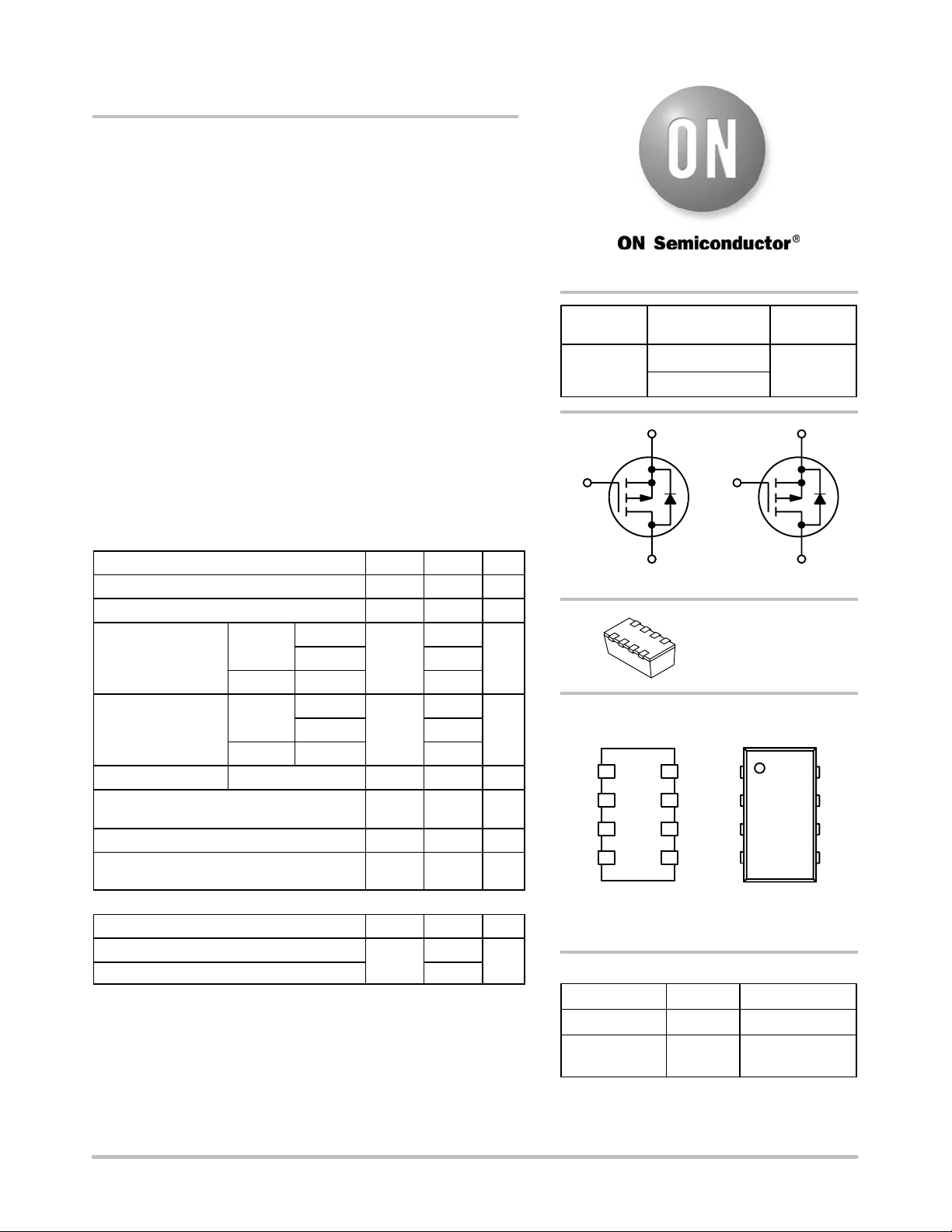
NTHD4401P
l
T
l
s
Power MOSFET
−20 V, −3.0 A, Dual P−Channel, ChipFETt
Features
• Low R
• Leadless ChipFET Package 40% Smaller Footprint than TSOP−6
• ChipFET Package with Excellent Thermal Capabilities where Heat
Transfer is Required
• Pb−Free Package is Available
Applications
• Charge Control in Battery Chargers
• Optimized for Battery and Load Management Applications in
Portable Equipment
• MP3 Players, Cell Phones, Digital Cameras, PDAs
• Buck and Boost DC−DC Converters
and Fast Switching Speed in a ChipFET Package
DS(on)
G
1
(BR)DSS
−20 V
http://onsemi.com
R
TYP
DS(on)
130 mW @ −4.5 V
200 mW @ −2.5 V
S
1
G
ID MAXV
−3.0 A
S
2
2
MAXIMUM RATINGS (T
Drain−to−Source Voltage V
Gate−to−Source Voltage V
Continuous Drain
Current (Note 1)
Power Dissipation
(Note 1)
Pulsed Drain Current
Operating Junction and Storage Temperature TJ, T
Source Current (Body Diode) I
Lead Temperature for Soldering Purposes
(1/8″ from case for 10 s)
= 25°C unless otherwise noted)
J
Rating Symbol Value Unit
stg
−20 V
"12 V
−2.1
1.1
−9.0 A
−55 to
150
−2.5 A
260 °C
A
W
°C
DSS
GS
Steady
State
t v 5 s TA = 25°C −3.0
Steady
State
t v 5 s TA = 25°C 2.1
TA = 25°C
TA = 85°C −1.5
TA = 25°C
TA = 85°C 0.6
tp = 10 ms
I
D
P
D
I
DM
S
T
L
THERMAL RESISTANCE RATINGS
Rating Symbol Value Unit
Junction−to−Ambient − Steady State (Note 1) R
Junction−to−Ambient − t v 5 s 60
Maximum ratings are those values beyond which device damage can occur.
Maximum ratings applied to the device are individual stress limit values (not
normal operating conditions) and are not valid simultaneously. If these limits are
exceeded, device functional operation is not implied, damage may occur and
reliability may be affected.
1. Surface Mounted on FR4 Board using 1 in sq pad size (Cu area = 1.27 in sq
[1 oz] including traces).
© Semiconductor Components Industries, LLC, 2005
November, 2005 − Rev. 4
q
JA
°C/W
110
1 Publication Order Number:
D
1
P−Channel MOSFET
PIN
CONNECTIONS
81
D
1
7
D
1
6
D
2
5
D
2
2
3
4
C4 = Specific Device Code
M = Month Code
G = Pb−Free Package
P−Channel MOSFE
ChipFET
CASE 1206A
STYLE 2
MARKING
DIAGRAM
S
1
1
2
G
1
S
2
G
2
G
3
4
C4 M
D
2
8
7
6
5
ORDERING INFORMATION
Device Package Shipping
NTHD4401PT1 ChipFET 3000/Tape & Ree
NTHD4401PT1G ChipFET
(Pb−Free)
†For information on tape and reel specifications,
including part orientation and tape sizes, please
refer to our Tape and Reel Packaging Specification
Brochure, BRD8011/D.
3000/Tape & Ree
NTHD4401P/D
†
Page 2
NTHD4401P
ELECTRICAL CHARACTERISTICS (T
= 25°C unless otherwise noted)
J
Characteristic Symbol Test Condition Min Typ Max Unit
OFF CHARACTERISTICS
Drain−to−Source Breakdown Voltage V
Drain−to−Source Breakdown Voltage Tem-
perature Coefficient
V
(Br)DSS/TJ
Zero Gate Voltage Drain Current I
(Br)DSS
DSS
VGS = 0 V, ID = −250 mA
VGS = 0 V TJ = 25°C −1.0 mA
VDS = −16 V TJ = 85°C −5.0
Gate−to−Source Leakage Current I
GSS
VDS = 0 V, VGS = "12 V "100 nA
ON CHARACTERISTICS (Note 2)
Gate Threshold Voltage V
Gate Threshold Temperature Coefficient V
Drain−to−Source On Resistance R
GS(th)
GS(th)/TJ
DS(on)
VGS = VDS, ID = −250 mA
VGS = −4.5 V, ID = −2.1 A
VGS = −2.5 V, ID = −1.7 A
VGS = −1.8 V, ID = −1.0 A
Forward Transconductance g
FS
VDS = −10 V, ID = −2.1 A 5.0 S
CHARGES, CAPACITANCES AND GATE RESISTANCE
Input Capacitance C
Output Capacitance C
Reverse Transfer Capacitance C
Total Gate Charge Q
Threshold Gate Charge Q
Gate−to−Source Charge Q
Gate−to−Drain Charge Q
iss
oss
rss
G(TOT)
G(TH)
GS
GD
VGS = 0 V, f = 1.0 MHz,
VDS = −10 V
VGS = −4.5 V, VDS = −10 V,
ID = −2.1 A
SWITCHING CHARACTERISTICS (Note 3)
Turn−On Delay Time t
Rise Time t
Turn−Off Delay Time t
Fall Time t
d(on)
r
d(off)
f
VGS = −4.5 V, VDD = −16 V,
ID = −2.1 A, RG = 2.5 W
DRAIN−SOURCE DIODE CHARACTERISTICS
Forward Diode Voltage V
SD
VGS = 0 V
IS = −2.5 A
Reverse Recovery Time t
Charge Time t
Discharge Time t
Reverse Recovery Charge Q
rr
a
b
RR
VGS = 0 V, dIS/dt = 90 A/ms,
IS = −2.1 A
2. Pulse Test: Pulse Width v 300 ms, Duty Cycle v 2%.
3. Switching characteristics are independent of operating junction temperatures.
−20 −23 V
−8.0 mV/°C
−0.6 −0.75 −1.2 V
2.65 mV/°C
0.130
0.200
0.155
0.240
0.34
185 300
95 150
30 50
3.0 6.0
0.2
0.5
0.9
7.0 12
13 25
33 50
27 40
−0.85 −1.15
32
10
22
15 nC
W
pF
nC
ns
V
ns
http://onsemi.com
2
Page 3
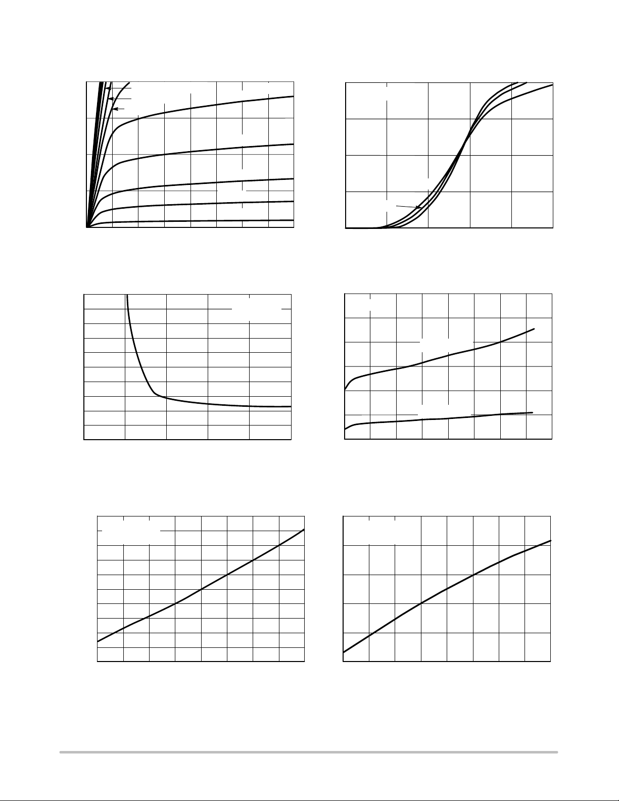
NTHD4401P
4
−2.2 V
3
2
1
DRAIN CURRENT (AMPS)
D,
−I
0
0
1
−VDS, DRAIN−TO−SOURCE VOLTAGE (VOLTS)
Figure 1. On−Region Characteristics
0.5
0.4
0.3
0.2
TYPICAL PERFORMANCE CURVES (T
VGS = −6 V to −3 V
VGS = −2.4 V
4
−2 V
−1.8 V
−1.6 V
−1.4 V
−1.2 V
5
TJ = 25°C
632
78
ID = −2.1 A
TJ = 25°C
= 25°C unless otherwise noted)
J
4
VDS ≥ −10 V
3
2
1
DRAIN CURRENT (AMPS)
D,
−I
TC = −55°C
25°C
0
0.5
1
−VGS, GATE−TO−SOURCE VOLTAGE (VOLTS)
Figure 2. Transfer Characteristics
0.25
TJ = 25°C
0.225
0.2
0.175
0.15
VGS = −2.5 V
100°C
21.5 2.5
3
0.1
DRAIN−TO−SOURCE RESISTANCE (W)
0
16
DS(on),
R
24
−VGS, GATE−TO−SOURCE VOLTAGE (VOLTS)
35
Figure 3. On−Resistance vs. Gate−to−Source
0.125
DRAIN−TO−SOURCE RESISTANCE (W)
0.1
0.5 4.5
DS(on),
R
1.5 2.5 3.5
−ID, DRAIN CURRENT (AMPS)
Figure 4. On−Resistance vs. Drain Current and
Voltage
VGS = −4.5 V
Gate Voltage
1.6
ID = −2.1 A
VGS = −4.5 V
1.4
ID = −1.0 A
VGS = −1.8 V
1.2
1.2
1
DRAIN−TO−SOURCE
0.8
DS(on),
R
RESISTANCE (NORMALIZED)
0.6
−50 0−25 25
Figure 5. On−Resistance Variation with
50 125100
75 150
TJ, JUNCTION TEMPERATURE (°C)
Temperature
1
DRAIN−TO−SOURCE
DS(on),
R
RESISTANCE (NORMALIZED)
0.8
−50 −25 0 25 50 75 100 125 150
TJ, JUNCTION TEMPERATURE (°C)
Figure 6. On−Resistance Variation with
Temperature
http://onsemi.com
3
Page 4

NTHD4401P
S)
−V
GATE−TO−SOURCE VOLTAGE (VOLTS)
0
−I
, LEAKAGE (A)
TYPICAL PERFORMANCE CURVES (T
10000
VGS = 0 V
TJ = 150°C
1000
DSS
100
TJ = 100°C
10
24 8
610 1814
12
−VDS, DRAIN−TO−SOURCE VOLTAGE (VOLTS)
Figure 7. Drain−to−Source Leakage Current
vs. Voltage
6
−V
DS
5
4
3
2
Q2Q1
1
0
GS,
02
1
Qg, TOTAL GATE CHARGE (nC)
QT
−V
GS
ID = −2.1 A
TJ = 25°C
1.50.5 3.5
32.5
= 25°C unless otherwise noted)
J
600
500
VDS = 0 V VGS = 0 V
C
iss
TJ = 25°C
400
C
rss
300
200
C, CAPACITANCE (pF)
100
0
2016
50
−VGS−V
510 10
DS
GATE−TO−SOURCE OR DRAIN−TO−SOURCE VOLTAGE (VOLT
Figure 8. Capacitance Variation
12
10
8
6
4
2
0
t, TIME (ns)
DRAIN−TO−SOURCE VOLTAGE (VOLTS)
DS,
−V
100
10
t
d(off)
t
d(on)
t
f
t
r
VDD = −16 V
ID = −2.1 A
VGS = −4.5 V
1
101
RG, GATE RESISTANCE (OHMS)
C
oss
15
20
10
Figure 9. Gate−to−Source and
Drain−to−Source Voltage vs. Total Charge
2.5
VGS = 0 V
TJ = 25°C
2
1.5
1
0.5
, SOURCE CURRENT (AMPS)
S
−I
0
−VSD, SOURCE−TO−DRAIN VOLTAGE (VOLTS)
Figure 11. Diode Forward Voltage vs. Current
http://onsemi.com
4
Figure 10. Resistive Switching Time Variation
vs. Gate Resistance
0.70.50.3
0.9
Page 5

NTHD4401P
1.0
D = 0.5
0.2
0.1
0.1
0.05
0.0175 Ω 0.0710 Ω 0.2706 Ω 0.5776 Ω 0.7086 Ω
0.02
0.01
r(t), NORMALIZED EFFECTIVE
SINGLE PULSE
TRANSIENT THERMAL RESISTANCE
0.01
1.0E−03 1.0E−02 1.0E−01 1.0E+00 1.0E+01 1.0E+02 1.0E+03
Chip
t, TIME (s)
Figure 12. Thermal Response
SOLDERING FOOTPRINT*
Normalized to θJA at 10s.
107.55 F1.7891 F0.3074 F0.0854 F0.0154 F
Ambient
0.457
0.018
0.66
0.026
2.032
0.08
0.711
0.028
SCALE 20:1
0.635
0.025
mm
ǒ
inches
0.635
0.025
0.457
0.018
Ǔ
0.66
0.026
2.032
0.08
Figure 13. Basic Figure 14. Style 2
*For additional information on our Pb−Free strategy and soldering
details, please download the ON Semiconductor Soldering and
Mounting Techniques Reference Manual, SOLDERRM/D.
0.254
0.010
SCALE 20:1
1.092
0.043
mm
ǒ
inches
0.178
0.007
Ǔ
BASIC PAD PATTERNS
The basic pad layout with dimensions is shown in
Figure 13. This is sufficient for low power dissipation
MOSFET applications, but power semiconductor
performance requires a greater copper pad area, particularly
for the drain leads.
The minimum recommended pad pattern shown in
Figure 14 improves the thermal area of the drain
connections (pins 5, 6, 7, 8) while remaining within the
ChipFET is a trademark of Vishay Siliconix.
http://onsemi.com
confines of the basic footprint. The drain copper area is
0.0019 sq. in. (or 1.22 sq. mm). This will assist the power
dissipation path away from the device (through the copper
leadframe) and into the board and exterior chassis (if
applicable) for the single device. The addition of a further
copper area and/or the addition of vias to other board layers
will enhance the performance still further.
5
Page 6

MECHANICAL CASE OUTLINE
PACKAGE DIMENSIONS
H
E
e1
STYLE 1:
PIN 1. DRAIN
2. DRAIN
3. DRAIN
4. GATE
5. SOURCE
6. DRAIN
7. DRAIN
8. DRAIN
8
1
SCALE 1:1
D
8765
1234
e
STYLE 2:
PIN 1. SOURCE 1
2. GATE 1
3. SOURCE 2
4. GATE 2
5. DRAIN 2
6. DRAIN 2
7. DRAIN 1
8. DRAIN 1
E
b
A
q
c
0.05 (0.002)
STYLE 3:
PIN 1. ANODE
2. ANODE
3. SOURCE
4. GATE
5. DRAIN
6. DRAIN
7. CATHODE
8. CATHODE
ChipFETt
CASE1206A−03
ISSUE K
L
RESET
STYLE 4:
PIN 1. COLLECTOR
2. COLLECTOR
3. COLLECTOR
4. BASE
5. EMITTER
6. COLLECTOR
7. COLLECTOR
8. COLLECTOR
8765
1234
STYLE 5:
PIN 1. ANODE
2. ANODE
3. DRAIN
4. DRAIN
5. SOURCE
6. GATE
7. CATHODE
8. CATHODE
DATE 19 MAY 2009
NOTES:
1. DIMENSIONING AND TOLERANCING PER ANSI Y14.5M, 1982.
2. CONTROLLING DIMENSION: MILLIMETER.
3. MOLD GATE BURRS SHALL NOT EXCEED 0.13 MM PER SIDE.
4. LEADFRAME TO MOLDED BODY OFFSET IN HORIZONTAL
AND VERTICAL SHALL NOT EXCEED 0.08 MM.
5. DIMENSIONS A AND B EXCLUSIVE OF MOLD GATE BURRS.
6. NO MOLD FLASH ALLOWED ON THE TOP AND BOTTOM LEAD
SURFACE.
DIMAMIN NOM MAX MIN
b 0.25 0.30 0.35 0.010
c 0.10 0.15 0.20 0.004
D 2.95 3.05 3.10 0.116
E 1.55 1.65 1.70 0.061
e 0.65 BSC
e1 0.55 BSC
L 0.28 0.35 0.42 0.011
H
E
q
MILLIMETERS
1.00 1.05 1.10 0.039
1.80 1.90 2.00 0.071 0.075 0.079
5° NOM
STYLE 6:
PIN 1. ANODE
2. DRAIN
3. DRAIN
4. GATE
5. SOURCE
6. DRAIN
7. DRAIN
8. CATHODE / DRAIN
INCHES
NOM MAX
0.041 0.043
0.012 0.014
0.006 0.008
0.120 0.122
0.065 0.067
0.025 BSC
0.022 BSC
0.014 0.017
5° NOM
SOLDERING FOOTPRINT
1
2.362
0.093
0.457
8X
0.018
DOCUMENT NUMBER:
DESCRIPTION:
2.032
0.08
0.65
0.025
PITCH
8X
*This information is generic. Please refer to
0.66
0.026
ǒ
inches
mm
Ǔ
Basic Style
OPTIONAL SOLDERING FOOTPRINTS ON PAGE 2
98AON03078D
ChipFET
Electronic versions are uncontrolled except when accessed directly from the Document Repository.
Printed versions are uncontrolled except when stamped “CONTROLLED COPY” in red.
GENERIC
MARKING DIAGRAM*
xxx MG
G
xxx = Specific Device Code
M = Month Code
G = Pb−Free Package
(Note: Microdot may be in either location)
device data sheet for actual part marking.
Pb−Free indicator, “G” or microdot “ G”,
may or may not be present.
PAGE 1 OF 2
ON Semiconductor and are trademarks of Semiconductor Components Industries, LLC dba ON Semiconductor or its subsidiaries in the United States and/or other countries.
ON Semiconductor reserves the right to make changes without further notice to any products herein. ON Semiconductor makes no warranty, representation or guarantee regarding
the suitability of its products for any particular purpose, nor does ON Semiconductor assume any liability arising out of the application or use of any product or circuit, and specifically
disclaims any and all liability, including without limitation special, consequential or incidental damages. ON Semiconductor does not convey any license under its patent rights nor the
rights of others.
© Semiconductor Components Industries, LLC, 2019
www.onsemi.com
Page 7

ChipFETt
CASE 1206A−03
ISSUE K
ADDITIONAL SOLDERING FOOTPRINTS*
DATE 19 MAY 2009
2.362
0.093
2X
0.457
0.018
2.032
1
0.08
2X
0.66
0.026
1.727
0.068
ǒ
inches
mm
1
0.457
4X
0.018
0.65
0.025
PITCH
0.66
0.026
Ǔ
Styles 1 and 4
2.032
0.08
1
2X
0.66
0.026
1
2.032
0.08
Style 2
2.032
0.08
2X4X
1.118
0.044
2X
0.66
0.026
2X
1.092
0.043
ǒ
inches
mm
2.362
0.093
Ǔ
1.092
0.043
2.362
0.093
0.65
0.025
PITCH
2X
0.457
0.018
1.118
0.044
ǒ
inches
mm
Ǔ
Style 3
*For additional information on our Pb−Free strategy and soldering
details, please download the ON Semiconductor Soldering and
Mounting Techniques Reference Manual, SOLDERRM/D.
DOCUMENT NUMBER:
DESCRIPTION:
ON Semiconductor and are trademarks of Semiconductor Components Industries, LLC dba ON Semiconductor or its subsidiaries in the United States and/or other countries.
ON Semiconductor reserves the right to make changes without further notice to any products herein. ON Semiconductor makes no warranty, representation or guarantee regarding
the suitability of its products for any particular purpose, nor does ON Semiconductor assume any liability arising out of the application or use of any product or circuit, and specifically
disclaims any and all liability, including without limitation special, consequential or incidental damages. ON Semiconductor does not convey any license under its patent rights nor the
rights of others.
98AON03078D
ChipFET
Electronic versions are uncontrolled except when accessed directly from the Document Repository.
Printed versions are uncontrolled except when stamped “CONTROLLED COPY” in red.
2.362
0.093
1.092
0.043
1.118
0.044
Style 5
2X
0.457
0.018
0.65
0.025
PITCH
mm
ǒ
Ǔ
inches
PAGE 2 OF 2
© Semiconductor Components Industries, LLC, 2019
www.onsemi.com
Page 8

ON Semiconductor and are trademarks of Semiconductor Components Industries, LLC dba ON Semiconductor or its subsidiaries in the United States and/or other countries.
ON Semiconductor owns the rights to a number of patents, trademarks, copyrights, trade secrets, and other intellectual property. A listing of ON Semiconductor’s product/patent
coverage may be accessed at www.onsemi.com/site/pdf/Patent−Marking.pdf
ON Semiconductor makes no warranty, representation or guarantee regarding the suitability of its products for any particular purpose, nor does ON Semiconductor assume any liability
arising out of the application or use of any product or circuit, and specifically disclaims any and all liability, including without limitation special, consequential or incidental damages.
Buyer is responsible for its products and applications using ON Semiconductor products, including compliance with all laws, regulations and safety requirements or standards,
regardless of any support or applications information provided by ON Semiconductor. “Typical” parameters which may be provided in ON Semiconductor data sheets and/or
specifications can and do vary in different applications and actual performance may vary over time. All operating parameters, including “Typicals” must be validated for each customer
application by customer’s technical experts. ON Semiconductor does not convey any license under its patent rights nor the rights of others. ON Semiconductor products are not
designed, intended, or authorized for use as a critical component in life support systems or any FDA Class 3 medical devices or medical devices with a same or similar classification
in a foreign jurisdiction or any devices intended for implantation in the human body. Should Buyer purchase or use ON Semiconductor products for any such unintended or unauthorized
application, Buyer shall indemnify and hold ON Semiconductor and its officers, employees, subsidiaries, affiliates, and distributors harmless against all claims, costs, damages, and
expenses, and reasonable attorney fees arising out of, directly or indirectly, any claim of personal injury or death associated with such unintended or unauthorized use, even if such
claim alleges that ON Semiconductor was negligent regarding the design or manufacture of the part. ON Semiconductor is an Equal Opportunity/Affirmative Action Employer. This
literature is subject to all applicable copyright laws and is not for resale in any manner.
. ON Semiconductor reserves the right to make changes without further notice to any products herein.
PUBLICATION ORDERING INFORMATION
LITERATURE FULFILLMENT:
Email Requests to: orderlit@onsemi.com
ON Semiconductor Website: www.onsemi.com
TECHNICAL SUPPORT
North American Technical Support:
Voice Mail: 1 800−282−9855 Toll Free USA/Canada
Phone: 011 421 33 790 2910
Europe, Middle East and Africa Technical Support:
Phone: 00421 33 790 2910
For additional information, please contact your local Sales Representative
◊
www.onsemi.com
1
 Loading...