

Page 1
NTA4151P, NTE4151P
MOSFET – Single,
P-Channel, Small Signal,
Gate Zener, SC-75, SC-89
-20 V, -760 mA
Features
• Low R
• Small Outline Package (1.6 x 1.6 mm)
• SC−75 Standard Gullwing Package
• ESD Protected Gate
• These Devices are Pb−Free, Halogen Free/BFR Free and are RoHS
Compliant
Applications
• High Side Load Switch
• DC−DC Conversion
• Small Drive Circuits
• Battery Operated Systems such as Cell Phones, PDAs, Digital
Cameras, etc.
MAXIMUM RATINGS (T
Drain−to−Source Voltage V
Gate−to−Source Voltage V
Continuous Drain Current
(Note 1)
Power Dissipation (Note 1)
Pulsed Drain Current
Operating Junction and Storage Temperature TJ,
Continuous Source Current (Body Diode) I
Lead Temperature for Soldering Purposes
(1/8 in from case for 10 s)
Gate−to−Source ESD Rating −
THERMAL RESISTANCE RATINGS
Junction−to−Ambient − Steady State (Note 1)
Stresses exceeding those listed in the Maximum Ratings table may damage the
device. If any of these limits are exceeded, device functionality should not be
assumed, damage may occur and reliability may be affected.
1. Surface mounted on FR4 board using 1 in sq pad size (Cu area = 1.127 in sq
[1 oz] including traces).
for Higher Efficiency and Longer Battery Life
DS(on)
= 25°C unless otherwise stated)
J
Parameter Symbol Value Units
DSS
GS
Steady State I
SC−75
SC−89
(Human Body Model, Method 3015)
Steady State
tp =10 ms
SC−75
SC−89
D
P
D
I
DM
T
STG
S
T
L
ESD 1800 V
R
q
JA
−20 V
±6.0 V
−760 mA
301
313
±1000 mA
−55 to
150
−250 mA
260 °C
415
400
mW
°C
°C/W
www.onsemi.com
R
TYP ID MAXV
(BR)DSS
−20 V
G
DS(on)
0.26 W @ −4.5 V
0.35 W @ −2.5 V
0.49 W @ −1.8 V
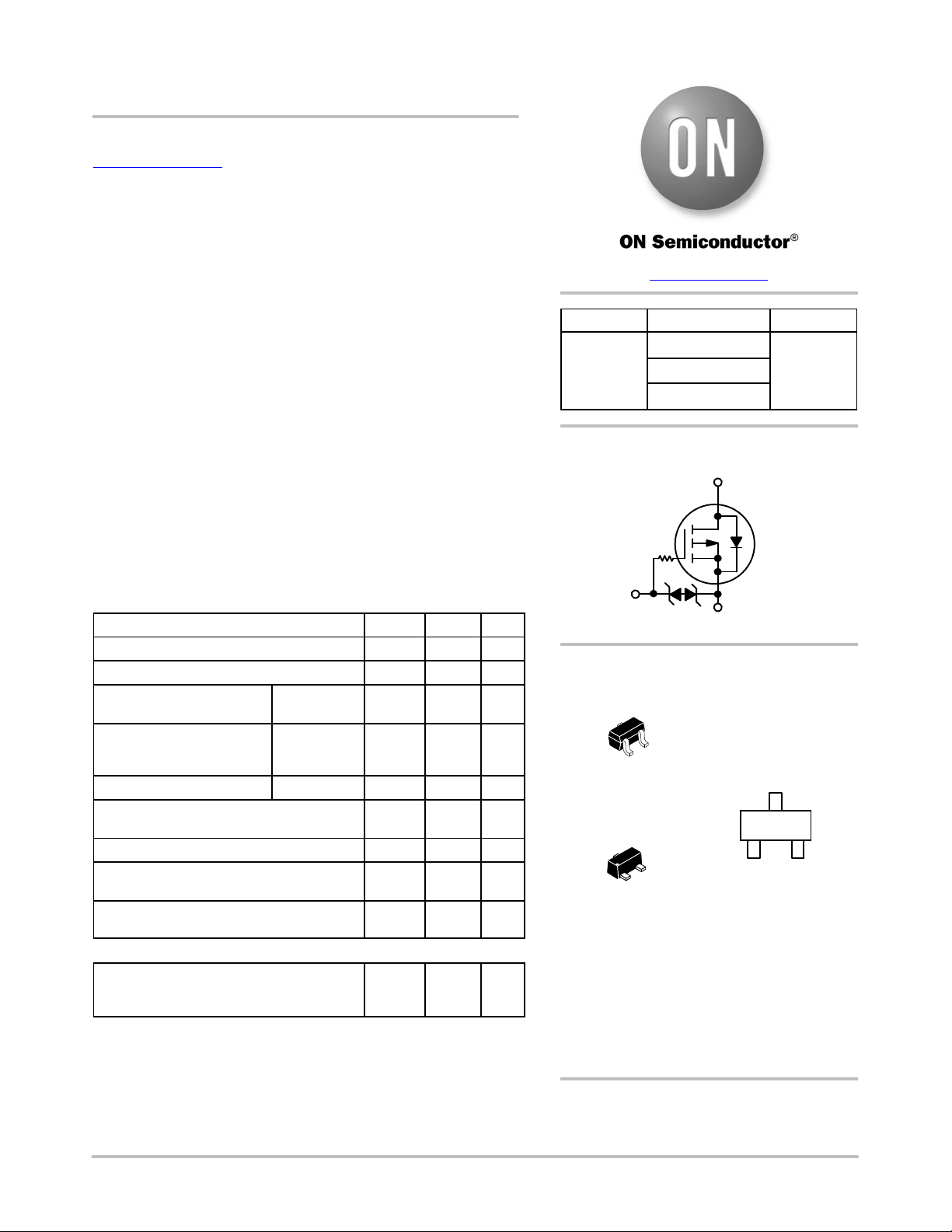
P−Channel MOSFET
D
S
−760 mA
MARKING DIAGRAM
& PIN ASSIGNMENT
3
2
SC−75 / SOT−416
*Date Code orientation may vary depending up-
1
CASE 463
STYLE 5
3
2
1
SC−89
CASE 463C
xx = Device Code
M = Date Code*
G = Pb−Free Package
(Note: Microdot may be in either location)
on manufacturing location.
1
Gate
3
Drain
xx M G
G
2
Source
ORDERING INFORMATION
See detailed ordering and shipping information in the package
dimensions section on page 2 of this data sheet.
© Semiconductor Components Industries, LLC, 2014
May, 2019 − Rev. 8
1 Publication Order Number:
NTA4151P/D
Page 2
NTA4151P, NTE4151P
ELECTRICAL CHARACTERISTICS (T
Parameter
= 25°C unless otherwise stated)
J
Symbol Test Condition Min Typ Max Unit
OFF CHARACTERISTICS
Drain−to−Source Breakdown Voltage
V
Zero Gate Voltage Drain Current I
Gate−to−Source Leakage Current I
(BR)DSS
DSS
GSS
V
V
V
GS
GS
DS
= 0 V, I
= 0 V, V
= 0 V, V
= −250 mA
D
= −16 V −1.0 −100 nA
DS
= ±4.5 V $1.0 $10
GS
−20 V
mA
ON CHARACTERISTICS (Note 2)
Gate Threshold Voltage
V
Drain−to−Source On Resistance R
Forward Transconductance g
GS(TH)
DS(on)
FS
V
= VGS, ID = −250 mA
DS
V
= −4.5 V, I
GS
V
= −2.5 V, I
GS
V
= −1.8 V, I
GS
V
= −10 V, I
DS
= −350 mA 0.26 0.36 W
D
= −300 mA 0.35 0.45
D
= −150 mA 0.49 1.0
D
= −250 mA 0.4 S
D
−0.45 −1.2 V
CHARGES AND CAPACITANCES
Input Capacitance C
Output Capacitance C
Reverse Transfer Capacitance C
Total Gate Charge Q
Threshold Gate Charge Q
Gate−to−Source Charge Q
Gate−to−Drain Charge Q
ISS
OSS
RSS
G(TOT)
G(TH)
GS
GD
= 0 V, f = 1.0 MHz,
GS
V
= −5.0 V
DS
V
= −4.5 V, VDD = −10 V,
GS
I
= −0.3 A
D
156
28
18
2.1
0.125
0.325
0.5
pF
nC
V
SWITCHING CHARACTERISTICS (Note 3)
Turn−On Delay Time td
Rise Time t
Turn−Off Delay Time td
Fall Time t
(ON)
r
(OFF)
f
V
= −4.5 V, V
GS
= −200 mA, R
I
D
= −10 V,
DD
G
= 10 W
8.0
8.2
29
20.4
ns
DRAIN−SOURCE DIODE CHARACTERISTICS
Forward Diode Voltage
V
SD
V
GS
= 0 V, I
= −250 mA −0.72 −1.1 V
S
Product parametric performance is indicated in the Electrical Characteristics for the listed test conditions, unless otherwise noted. Product
performance may not be indicated by the Electrical Characteristics if operated under different conditions.
2. Pulse Test: pulse width ≤ 300 ms, duty cycle ≤ 2%.
3. Switching characteristics are independent of operating junction temperatures.
ORDERING INFORMATION
Device Marking Package Shipping
NTA4151PT1G TN SC−75
3000 / Tape & Reel
(Pb−Free)
NTE4151PT1G TM SC−89
3000 / Tape & Reel
(Pb−Free)
†For information on tape and reel specifications, including part orientation and tape sizes, please refer to our Tape and Reel Packaging
Specifications Brochure, BRD8011/D.
†
www.onsemi.com
2
Page 3
NTA4151P, NTE4151P
R
DRAIN
TO
SOURCE
TYPICAL ELECTRICAL CHARACTERISTICS
0.7
0.6
−1.5 V
0.5
VGS = −1.75 V to −4.5 V
0.4
0.3
0.2
DRAIN CURRENT (AMPS)
D,
0.1
−I
0
0 0.5 1.0 1.5 2.0 2.5 3.0
−V
, DRAIN−TO−SOURCE VOLTAGE (VOLTS)
DS
Figure 1. On−Region Characteristics
0.6
VGS = −4.5 V
0.5
0.4
0.3
0.2
TJ = 125°C
TJ = 25°C
TJ = −55°C
TJ = 25°C
−1.25 V
−1.0 V
0.6
VDS w −10 V
0.5
0.4
0.3
0.2
DRAIN CURRENT (AMPS)
0.1
D,
−I
0
0 0.4 0.8 1.2 1.6 2.0
TJ = 125°C
TJ = 25°C
TJ = −55°C
−VGS, GATE−TO−SOURCE VOLTAGE (VOLTS)
Figure 2. Transfer Characteristics
0.6
VGS = −2.5 V
0.5
0.4
0.3
0.2
TJ = 125°C
TJ = 25°C
TJ = −55°C
0.1
DRAIN−TO−SOURCE RESISTANCE (W)
0
0 0.1 0.2 0.3 0.4 0.5 0.6 0.7
DS(on),
R
−ID, DRAIN CURRENT (AMPS)
Figure 3. On−Resistance vs. Drain Current and
Temperature
1.6
ID = − 0.35 A
= −4.5 V
V
GS
1.4
−
1.2
−
1.0
0.8
DS(on),
RESISTANCE (NORMALIZED)
0.6
−50 −25 0 25 50 75 100 125 150
TJ, JUNCTION TEMPERATURE (°C)
Figure 5. On−Resistance Variation with
Temperature
0.1
DRAIN−TO−SOURCE RESISTANCE (W)
0
0 0.1 0.2 0.3 0.4 0.5 0.6 0.7
DS(on),
R
−I
DRAIN CURRENT (AMPS)
D,
Figure 4. On−Resistance vs. Drain Current and
Temperature
250
TJ = 25°C
200
C
ISS
150
100
C, CAPACITANCE (pF)
50
0
0 4 8 12 16 20
C
RSS
C
OSS
DRAIN−TO−SOURCE VOLTAGE (VOLTS)
Figure 6. Capacitance Variation
www.onsemi.com
3
Page 4

NTA4151P, NTE4151P
TYPICAL ELECTRICAL CHARACTERISTICS
5
Q
T
4
3
Q
2
GS
Q
GD
1
GATE−TO−SOURCE VOLTAGE (VOLTS)
0
GS,
0 1.6
−V
0.4
0.8
Q
, TOTAL GATE CHARGE (nC)
G
1.2
Figure 7. Gate−to−Source Voltage vs. Total
Gate Charge
1.0
D = 0.5
0.2
0.1
0.1
0.05
VDS = −10 V
= −0.3 A
I
D
T
= 25°C
A
2.0 2.4
0.7
VGS = 0 V
0.6
0.5
0.4
0.3
0.2
, SOURCE CURRENT (AMPS)
0.1
S
−I
0
0 0.2 0.4 0.6 0.8 1.0
TJ = 125°C
TJ = 25°C
−VSD, SOURCE−TO−DRAIN VOLTAGE (VOLTS)
Figure 8. Diode Forward Voltage vs. Current
0.02
0.01
0.01
SINGLE PULSE
0.001
0.00001 0.0001 0.001 0.01 0.1 1.0 10 100 1000
r(t), NORMALIZED TRANSIENT THERMAL RESISTANCE
t, TIME (s)
Figure 9. Normalized Thermal Response
www.onsemi.com
4
Page 5
MECHANICAL CASE OUTLINE
PACKAGE DIMENSIONS
3
1
SCALE 4:1
2
3 PL
b
0.20 (0.008) D
M
C
STYLE 1:
PIN 1. BASE
2. EMITTER
3. COLLECTOR
STYLE 4:
PIN 1. CATHODE
2. CATHODE
3. ANODE
−E−
2
3
1
L
STYLE 2:
PIN 1. ANODE
2. N/C
3. CATHODE
STYLE 5:
PIN 1. GATE
2. SOURCE
3. DRAIN
SC−75/SOT−416
CASE 463−01
ISSUE G
DATE 07 AUG 2015
NOTES:
1. DIMENSIONING AND TOLERANCING PER ANSI
Y14.5M, 1982.
2. CONTROLLING DIMENSION: MILLIMETER.
MILLIMETERS
e
−D−
0.20 (0.008) E
H
E
A
DIM MIN NOM MAX
A 0.70 0.80 0.90
A1 0.00 0.05 0.10
b
0.15 0.20 0.30 0.006 0.008 0.012
C 0.10 0.15 0.25
D 1.55 1.60 1.65
E
0.70 0.80 0.90 0.027 0.031 0.035
e 1.00 BSC
L 0.10 0.15 0.20
H
1.50 1.60 1.70
E
GENERIC
INCHES
MIN NOM MAX
0.027 0.031 0.035
0.000 0.002 0.004
0.004 0.006 0.010
0.061 0.063 0.065
0.04 BSC
0.004 0.006 0.008
0.060 0.063 0.067
MARKING DIAGRAM*
A1
XX M
STYLE 3:
PIN 1. ANODE
2. ANODE
3. CATHODE
XX = Specific Device Code
G
1
M = Date Code
G = Pb−Free Package
*This information is generic. Please refer to
device data sheet for actual part marking.
Pb−Free indicator, “G” or microdot “ G”,
may or may not be present.
SOLDERING FOOTPRINT*
0.356
0.014
1.803
0.071
0.508
0.020
0.787
0.031
1.000
0.039
SCALE 10:1
ǒ
inches
mm
Ǔ
*For additional information on our Pb−Free strategy and soldering
details, please download the ON Semiconductor Soldering and
Mounting Techniques Reference Manual, SOLDERRM/D.
DOCUMENT NUMBER:
DESCRIPTION:
ON Semiconductor and are trademarks of Semiconductor Components Industries, LLC dba ON Semiconductor or its subsidiaries in the United States and/or other countries.
ON Semiconductor reserves the right to make changes without further notice to any products herein. ON Semiconductor makes no warranty, representation or guarantee regarding
the suitability of its products for any particular purpose, nor does ON Semiconductor assume any liability arising out of the application or use of any product or circuit, and specifically
disclaims any and all liability, including without limitation special, consequential or incidental damages. ON Semiconductor does not convey any license under its patent rights nor the
rights of others.
© Semiconductor Components Industries, LLC, 2019
98ASB15184C
SC−75/SOT−416
Electronic versions are uncontrolled except when accessed directly from the Document Repository.
Printed versions are uncontrolled except when stamped “CONTROLLED COPY” in red.
PAGE 1 OF 1
www.onsemi.com
Page 6

MECHANICAL CASE OUTLINE
PACKAGE DIMENSIONS
SCALE 4:1
SC−89, 3 LEAD
CASE 463C−03
ISSUE C DATE 31 JUL 2003
K
M
STYLE 1:
PIN 1. BASE
A
−X−
3
12
G
2 PL
0.08 (0.003) X
2. EMITTER
3. COLLECTOR
B
−Y−
3 PL
D
M
C
STYLE 2:
PIN 1. ANODE
2. N/C
3. CATHOD-
E
S
Y
N
J
−T−
STYLE 3:
PIN 1. ANODE
2. ANODE
3. CATHODE
H
H
L
G
RECOMMENDED PATTERN
OF SOLDER PADS
SEATING
PLANE
STYLE 4:
PIN 1. CATHODE
2. CATHODE
3. ANODE
NOTES:
1. DIMENSIONING AND TOLERANCING PER ANSI
Y14.5M, 1982.
2. CONTROLLING DIMENSION: MILLIMETERS
3. MAXIMUM LEAD THICKNESS INCLUDES LEAD
FINISH THICKNESS. MINIMUM LEAD THICKNESS
IS THE MINIMUM THICKNESS OF BASE
MATERIAL.
4. 463C−01 OBSOLETE, NEW STANDARD 463C−02.
MILLIMETERS
DIMAMIN NOM MIN NOM
1.50 1.60 1.70 0.059
B 0.75 0.85 0.95 0.030
C 0.60 0.70 0.80 0.024
D 0.23 0.28 0.33 0.009
G 0.50 BSC
H 0.53 REF
J 0.10 0.15 0.20 0.004
K 0.30 0.40 0.50 0.012
L 1.10 REF
M −−− −−− 10 −−−
N −−− −−− 10 −−−
S 1.50 1.60 1.70 0.059
MAX MAX
INCHES
0.063 0.067
0.034 0.040
0.028 0.031
0.011 0.013
0.020 BSC
0.021 REF
0.006 0.008
0.016 0.020
0.043 REF
_
_
−−− 10
−−− 10
0.063 0.067
GENERIC
MARKING DIAGRAM*
3
xx D
1
2
xx = Specific Device Code
D = Date Code
*This information is generic. Please refer to
device data sheet for actual part
marking.
_
_
DOCUMENT NUMBER:
DESCRIPTION:
ON Semiconductor and are trademarks of Semiconductor Components Industries, LLC dba ON Semiconductor or its subsidiaries in the United States and/or other countries.
ON Semiconductor reserves the right to make changes without further notice to any products herein. ON Semiconductor makes no warranty, representation or guarantee regarding
the suitability of its products for any particular purpose, nor does ON Semiconductor assume any liability arising out of the application or use of any product or circuit, and specifically
disclaims any and all liability, including without limitation special, consequential or incidental damages. ON Semiconductor does not convey any license under its patent rights nor the
rights of others.
© Semiconductor Components Industries, LLC, 2019
98AON11472D
SC−89, 3 LEAD
Electronic versions are uncontrolled except when accessed directly from the Document Repository.
Printed versions are uncontrolled except when stamped “CONTROLLED COPY” in red.
PAGE 1 OF 1
www.onsemi.com
Page 7

ON Semiconductor and are trademarks of Semiconductor Components Industries, LLC dba ON Semiconductor or its subsidiaries in the United States and/or other countries.
ON Semiconductor owns the rights to a number of patents, trademarks, copyrights, trade secrets, and other intellectual property. A listing of ON Semiconductor’s product/patent
coverage may be accessed at www.onsemi.com/site/pdf/Patent−Marking.pdf
ON Semiconductor makes no warranty, representation or guarantee regarding the suitability of its products for any particular purpose, nor does ON Semiconductor assume any liability
arising out of the application or use of any product or circuit, and specifically disclaims any and all liability, including without limitation special, consequential or incidental damages.
Buyer is responsible for its products and applications using ON Semiconductor products, including compliance with all laws, regulations and safety requirements or standards,
regardless of any support or applications information provided by ON Semiconductor. “Typical” parameters which may be provided in ON Semiconductor data sheets and/or
specifications can and do vary in different applications and actual performance may vary over time. All operating parameters, including “Typicals” must be validated for each customer
application by customer’s technical experts. ON Semiconductor does not convey any license under its patent rights nor the rights of others. ON Semiconductor products are not
designed, intended, or authorized for use as a critical component in life support systems or any FDA Class 3 medical devices or medical devices with a same or similar classification
in a foreign jurisdiction or any devices intended for implantation in the human body. Should Buyer purchase or use ON Semiconductor products for any such unintended or unauthorized
application, Buyer shall indemnify and hold ON Semiconductor and its officers, employees, subsidiaries, affiliates, and distributors harmless against all claims, costs, damages, and
expenses, and reasonable attorney fees arising out of, directly or indirectly, any claim of personal injury or death associated with such unintended or unauthorized use, even if such
claim alleges that ON Semiconductor was negligent regarding the design or manufacture of the part. ON Semiconductor is an Equal Opportunity/Affirmative Action Employer. This
literature is subject to all applicable copyright laws and is not for resale in any manner.
. ON Semiconductor reserves the right to make changes without further notice to any products herein.
PUBLICATION ORDERING INFORMATION
LITERATURE FULFILLMENT:
Email Requests to: orderlit@onsemi.com
ON Semiconductor Website: www.onsemi.com
TECHNICAL SUPPORT
North American Technical Support:
Voice Mail: 1 800−282−9855 Toll Free USA/Canada
Phone: 011 421 33 790 2910
Europe, Middle East and Africa Technical Support:
Phone: 00421 33 790 2910
For additional information, please contact your local Sales Representative
◊
www.onsemi.com
1
 Loading...