

Page 1
NTA4001N, NVA4001N
MOSFET – Single,
N-Channel, Gate ESD
Protection, Small Signal,
SC-75
20 V, 238 mA
Features
• Low Gate Charge for Fast Switching
• Small 1.6 x 1.6 mm Footprint
• ESD Protected Gate
• AEC−Q101 Qualified and PPAP Capable − NVA4001N
• These Devices are Pb−Free and are RoHS Compliant
http://onsemi.com
V
(BR)DSS
20 V 238 mA
R
DS(on)
Typ @ V
1.5 W @ 4.5 V
2.2 W @ 2.5 V
GS
3
ID MAX
(Note 1)
Applications
• Power Management Load Switch
• Level Shift
• Portable Applications such as Cell Phones, Media Players,
Digital Cameras, PDA’s, Video Games, Hand Held Computers, etc.
MAXIMUM RATINGS (T
Parameter
Drain−to−Source Voltage V
Gate−to−Source Voltage V
Continuous Drain
Current (Note 1)
Power Dissipation
(Note 1)
Pulsed Drain Current
Operating Junction and Storage Temperature TJ,
Continuous Source Current (Body Diode) I
Lead Temperature for Soldering Purposes
(1/8” from case for 10 s)
Stresses exceeding Maximum Ratings may damage the device. Maximum
Ratings are stress ratings only. Functional operation above the Recommended
Operating Conditions is not implied. Extended exposure to stresses above the
Recommended Operating Conditions may affect device reliability.
= 25°C unless otherwise stated)
J
Symbol Value Unit
DSS
GS
Steady State = 25°C I
Steady State = 25°C P
tP v 10 ms
T
I
DM
STG
SD
T
D
D
L
20 V
±10 V
238 mA
300 mW
714 mA
−55 to
150
238 mA
260 °C
°C
1
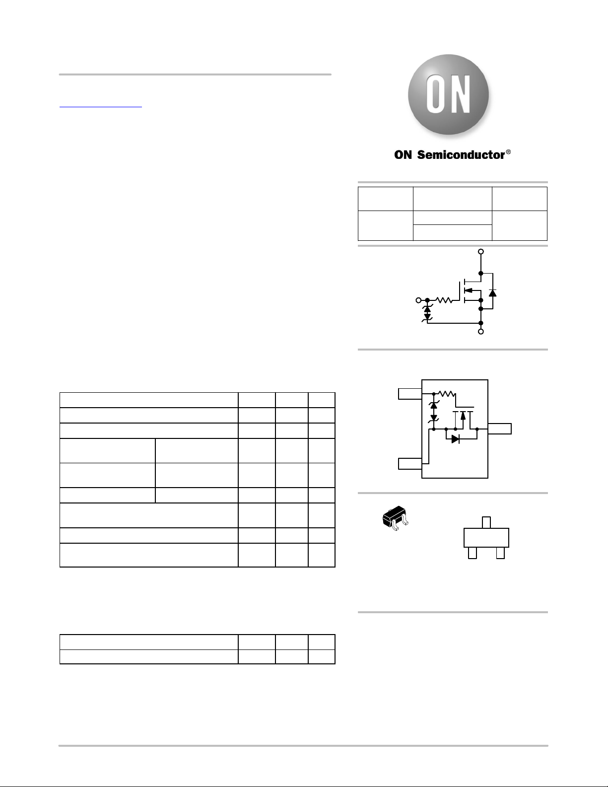
PIN CONNECTIONS
Gate31
Source
SC−75 / SOT−416
CASE 463
2
3
2
1
STYLE 5
TF = Specific Device Code
M = Date Code
G = Pb−Free Package
(Note: Microdot may be in either location)
N−Channel
SC−75 (3−Leads)
(Top View)
MARKING DIAGRAM
TF MG
1
2
Drain
3
G
2
THERMAL RESISTANCE RATINGS
Parameter Symbol Max Unit
Junction−to−Ambient – Steady State (Note 1)
1. Surface−mounted on FR4 board using 1 in sq. pad size (Cu area = 1.127 in sq.
[1 oz] including traces).
© Semiconductor Components Industries, LLC, 2011
May, 2019 − Rev. 2
R
q
JA
416 °C/W
1 Publication Order Number:
ORDERING INFORMATION
See detailed ordering and shipping information in the package
dimensions section on page 4 of this data sheet.
NTA4001N/D
Page 2
NTA4001N, NVA4001N
ELECTRICAL CHARACTERISTICS (T
Parameter
= 25°C unless otherwise specified)
J
Symbol Test Condition Min Typ Max Unit
OFF CHARACTERISTICS
Drain−to−Source Breakdown Voltage
Zero Gate Voltage Drain Current I
Gate−to−Source Leakage Current I
V
(BR)DSS
DSS
GSS
VGS = 0 V, ID = 100 mA
VGS = 0 V, VDS = 20 V 1.0
VDS = 0 V, VGS = ±10 V ±100
ON CHARACTERISTICS (Note 2)
Gate Threshold Voltage
Drain−to−Source On Resistance R
V
GS(TH)
DS(on)
VDS = 3 V, ID = 100 mA
VGS = 4.5 V, ID = 10 mA 1.5 3.0
VGS = 2.5 V, ID = 10 mA 2.2 3.5
Forward Transconductance g
FS
CAPACITANCES
Input Capacitance
Output Capacitance C
Reverse Transfer Capacitance C
C
ISS
OSS
RSS
SWITCHING CHARACTERISTICS (Note 3)
Turn−On Delay Time
Rise Time t
Turn−Off Delay Time t
Fall Time t
t
d(ON)
r
d(OFF)
f
VGS = 4.5 V, VDS = 5 V,
I
DRAIN−SOURCE DIODE CHARACTERISTICS
Forward Diode Voltage
V
SD
2. Pulse Test: pulse width v 300 ms, duty cycle v 2%.
3. Switching characteristics are independent of operating junction temperatures.
20 V
mA
mA
0.5 1.0 1.5 V
W
VDS = 3 V, ID = 10 mA 80 mS
11.5 20
VDS = 5 V, f = 1 MHz,
V
= 0 V
GS
10 15
pF
3.5 6.0
13 ns
15
= 10 mA, RG = 10 W
D
98
ns
60
VGS = 0 V, IS = 10 mA 0.66 0.8 V
http://onsemi.com
2
Page 3

NTA4001N, NVA4001N
TYPICAL PERFORMANCE CURVES
0.2
0.18
0.16
0.14
0.12
0.1
0.08
0.06
, DRAIN CURRENT (A)
D
I
0.04
0.02
0
0 0.4 0.8 1.2 1.6 2
VDS, DRAIN−TO−SOURCE VOLTAGE (V)
VGS = 10 V
VGS = 5 V
VGS = 2.8 V
VGS = 2.4 V
VGS = 1.2 V
VGS = 2 V
.
Figure 1. On−region Characteristics
2.5
VGS = 4.5 V
2
1.5
TJ = 125°C
TJ = 25°C
TJ = 25°C
VGS = 1.4 V
0.2
VDS = 5 V
0.16
0.12
0.08
, DRAIN CURRENT (A)
D
0.04
I
0
0.6 0.8 1 1.2 1.4 1.6 1.8 2
, GATE−TO−SOURCE VOLTAGE (V)
V
GS
TJ = 125°C
Figure 2. Transfer Characteristics
2.5
TJ = 25°C
VGS = 2.5 V
2
1.5
VGS = 4.5 V
TJ = 25°C
TJ = −55°C
, DRAIN−TO−SOURCE
RESISTANCE (W)
1
(on)
RDS
0.5
0 0.05 0.1 0.15 0.2
TJ = −55°C
ID, DRAIN CURRENT (A)
Figure 3. On−resistance versus Drain Current
and Temperature
2
ID = 0.01 A
1.8
VGS = 4.5 V
1.6
1.4
1.2
1
0.8
, DRAIN−TO−SOURCE
0.6
(on)
0.4
RESISTANCE (NORMALIZED)
RDS
0.2
0
−50 −25 0 25 50 75 100 125 150
TJ, JUNCTION TEMPERATURE (°C)
, DRAIN−TO−SOURCE
RESISTANCE (W)
1
(on)
RDS
0.5
0 0.05 0.1 0.15 0.2
ID, DRAIN CURRENT (A)
Figure 4. On−resistance versus Drain Current
and Gate Voltage
1000
, LEAKAGE (nA)
DSS
I
VGS = 0 V
100
10
1
0 5 10 15 20
VDS, DRAIN−TO−SOURCE VOLTAGE (V)
TJ = 150°C
TJ = 125°C
Figure 5. On−resistance Variation with
Temperature
http://onsemi.com
Figure 6. Drain−to−Source Leakage Current
versus Voltage
3
Page 4

NTA4001N, NVA4001N
TYPICAL PERFORMANCE CURVES
25
Ciss
TJ = 25°C
20
Crss
15
10
C, CAPACITANCE (pF)
5
V
0
VDS = 0 V
GS
= 0 V
10 5 0 5 10 15 20
VDS
V
GS
GATE−TO−SOURCE OR DRAIN−TO−SOURCE
VOLTAGE (V)
Figure 7. Capacitance Variation
0.1
V
= 0 V
GS
0.08
TJ = 25°C
Ciss
Coss
Crss
1000
VDD = 5 V
= 10 mA
I
D
V
= 4.5 V
GS
t
d(off)
t
d(on)
t
f
t
r
t, TIME (ns)
100
10
1
1 10 100
R
, GATE RESISTANCE (W)
G
Figure 8. Resistive Switching Time Variation
versus Gate Resistance
0.06
0.04
, SOURCE CURRENT (A)
0.02
S
I
0
0.5 0.55 0.6 0.65 0.7 0.75 0.8
, SOURCE−TO−DRAIN VOLTAGE (V)
V
SD
Figure 9. Diode Forward Voltage
versus Current
ORDERING INFORMATION
Order Number Package Shipping
NTA4001NT1G SC−75
3000 / Tape & Reel
(Pb−Free)
NVA4001NT1G SC−75
3000 / Tape & Reel
(Pb−Free)
†For information on tape and reel specifications, including part orientation and tape sizes, please refer to our Tape and Reel Packaging
Specifications Brochure, BRD8011/D.
†
http://onsemi.com
4
Page 5

MECHANICAL CASE OUTLINE
PACKAGE DIMENSIONS
3
1
SCALE 4:1
2
3 PL
b
0.20 (0.008) D
M
C
STYLE 1:
PIN 1. BASE
2. EMITTER
3. COLLECTOR
STYLE 4:
PIN 1. CATHODE
2. CATHODE
3. ANODE
−E−
2
3
1
L
STYLE 2:
PIN 1. ANODE
2. N/C
3. CATHODE
STYLE 5:
PIN 1. GATE
2. SOURCE
3. DRAIN
SC−75/SOT−416
CASE 463−01
ISSUE G
DATE 07 AUG 2015
NOTES:
1. DIMENSIONING AND TOLERANCING PER ANSI
Y14.5M, 1982.
2. CONTROLLING DIMENSION: MILLIMETER.
MILLIMETERS
e
−D−
0.20 (0.008) E
H
E
A
DIM MIN NOM MAX
A 0.70 0.80 0.90
A1 0.00 0.05 0.10
b
0.15 0.20 0.30 0.006 0.008 0.012
C 0.10 0.15 0.25
D 1.55 1.60 1.65
E
0.70 0.80 0.90 0.027 0.031 0.035
e 1.00 BSC
L 0.10 0.15 0.20
H
1.50 1.60 1.70
E
GENERIC
INCHES
MIN NOM MAX
0.027 0.031 0.035
0.000 0.002 0.004
0.004 0.006 0.010
0.061 0.063 0.065
0.04 BSC
0.004 0.006 0.008
0.060 0.063 0.067
MARKING DIAGRAM*
A1
XX M
STYLE 3:
PIN 1. ANODE
2. ANODE
3. CATHODE
XX = Specific Device Code
G
1
M = Date Code
G = Pb−Free Package
*This information is generic. Please refer to
device data sheet for actual part marking.
Pb−Free indicator, “G” or microdot “ G”,
may or may not be present.
SOLDERING FOOTPRINT*
0.356
0.014
1.803
0.071
0.508
0.020
0.787
0.031
1.000
0.039
SCALE 10:1
ǒ
inches
mm
Ǔ
*For additional information on our Pb−Free strategy and soldering
details, please download the ON Semiconductor Soldering and
Mounting Techniques Reference Manual, SOLDERRM/D.
DOCUMENT NUMBER:
DESCRIPTION:
ON Semiconductor and are trademarks of Semiconductor Components Industries, LLC dba ON Semiconductor or its subsidiaries in the United States and/or other countries.
ON Semiconductor reserves the right to make changes without further notice to any products herein. ON Semiconductor makes no warranty, representation or guarantee regarding
the suitability of its products for any particular purpose, nor does ON Semiconductor assume any liability arising out of the application or use of any product or circuit, and specifically
disclaims any and all liability, including without limitation special, consequential or incidental damages. ON Semiconductor does not convey any license under its patent rights nor the
rights of others.
© Semiconductor Components Industries, LLC, 2019
98ASB15184C
SC−75/SOT−416
Electronic versions are uncontrolled except when accessed directly from the Document Repository.
Printed versions are uncontrolled except when stamped “CONTROLLED COPY” in red.
PAGE 1 OF 1
www.onsemi.com
Page 6

ON Semiconductor and are trademarks of Semiconductor Components Industries, LLC dba ON Semiconductor or its subsidiaries in the United States and/or other countries.
ON Semiconductor owns the rights to a number of patents, trademarks, copyrights, trade secrets, and other intellectual property. A listing of ON Semiconductor’s product/patent
coverage may be accessed at www.onsemi.com/site/pdf/Patent−Marking.pdf
ON Semiconductor makes no warranty, representation or guarantee regarding the suitability of its products for any particular purpose, nor does ON Semiconductor assume any liability
arising out of the application or use of any product or circuit, and specifically disclaims any and all liability, including without limitation special, consequential or incidental damages.
Buyer is responsible for its products and applications using ON Semiconductor products, including compliance with all laws, regulations and safety requirements or standards,
regardless of any support or applications information provided by ON Semiconductor. “Typical” parameters which may be provided in ON Semiconductor data sheets and/or
specifications can and do vary in different applications and actual performance may vary over time. All operating parameters, including “Typicals” must be validated for each customer
application by customer’s technical experts. ON Semiconductor does not convey any license under its patent rights nor the rights of others. ON Semiconductor products are not
designed, intended, or authorized for use as a critical component in life support systems or any FDA Class 3 medical devices or medical devices with a same or similar classification
in a foreign jurisdiction or any devices intended for implantation in the human body. Should Buyer purchase or use ON Semiconductor products for any such unintended or unauthorized
application, Buyer shall indemnify and hold ON Semiconductor and its officers, employees, subsidiaries, affiliates, and distributors harmless against all claims, costs, damages, and
expenses, and reasonable attorney fees arising out of, directly or indirectly, any claim of personal injury or death associated with such unintended or unauthorized use, even if such
claim alleges that ON Semiconductor was negligent regarding the design or manufacture of the part. ON Semiconductor is an Equal Opportunity/Affirmative Action Employer. This
literature is subject to all applicable copyright laws and is not for resale in any manner.
. ON Semiconductor reserves the right to make changes without further notice to any products herein.
PUBLICATION ORDERING INFORMATION
LITERATURE FULFILLMENT:
Email Requests to: orderlit@onsemi.com
ON Semiconductor Website: www.onsemi.com
TECHNICAL SUPPORT
North American Technical Support:
Voice Mail: 1 800−282−9855 Toll Free USA/Canada
Phone: 011 421 33 790 2910
Europe, Middle East and Africa Technical Support:
Phone: 00421 33 790 2910
For additional information, please contact your local Sales Representative
◊
www.onsemi.com
1
 Loading...