

Page 1
NSR05T40XV2
s
500 mA, 40 V Schottky
Barrier Diode
These Schottky barrier diodes are optimized for low forward
voltage drop and low leakage current that offers the most optimal
power dissipation in applications. They are housed in spacing saving
micro−packaging ideal for space constraint applications.
www.onsemi.com
Features
• Low Forward Voltage Drop − 530 mV (Typ.) @ I
• Low Reverse Current − 3.0 mA (Typ.) @ V
= 40 V
R
= 500 mA
F
• 500 mA of Continuous Forward Current
• ESD Rating: − Human Body Model: Class 3B
− Charged Device Model: Class IV
• High Switching Speed
• These Devices are Pb−Free, Halogen Free/BFR Free and are RoHS
Compliant
Typical Applications
• LCD and Keypad Backlighting
• Camera Photo Flash
• Buck and Boost dc−dc Converters
• Reverse Voltage and Current Protection
• Clamping & Protection
MAXIMUM RATINGS
Rating Symbol Value Unit
Reverse Voltage V
Forward Current (DC) I
Forward Surge Current
(60 Hz @ 1 cycle)
Repetitive Peak Forward Current
(Pulse Wave = 1 sec, Duty Cycle = 66%)
ESD Rating: Human Body Model
Charged Device Model
Stresses exceeding those listed in the Maximum Ratings table may damage the
device. If any of these limits are exceeded, device functionality should not be
assumed, damage may occur and reliability may be affected.
R
F
I
FSM
I
FRM
ESD > 8
40 V
500 mA
3.0 A
1.5 A
kV
> 1
2
1
SOD−523
CASE 502
YK = Specific Device Code
M Date Code
1
CATHODE
ORDERING INFORMATION
Device Package Shipping†
NSR05T40XV2T5G SOD−523
(Pb−Free)
†For information on tape and reel specifications,
including part orientation and tape sizes, please
refer to our Tape and Reel Packaging Specification
Brochure, BRD801 1/D.
MARKING
DIAGRAM
YK
M
12
2
ANODE
8000 / Tape &
Reel
© Semiconductor Components Industries, LLC, 2017
February, 2017 − Rev. 1
1 Publication Order Number:
NSR05T40XV2/D
Page 2
NSR05T40XV2
1000
0
R(t) (
C/W)
THERMAL CHARACTERISTICS
Characteristic Symbol Min Typ Max Unit
Thermal Resistance
Junction−to−Ambient (Note 1)
Total Power Dissipation @ T
= 25°C
A
Thermal Resistance
Junction−to−Ambient (Note 2)
Total Power Dissipation @ T
= 25°C
A
Junction and Storage Temperature Range TJ, T
1. Mounted onto a 4 in square FR−4 board 50 mm sq. 1 oz. Cu 0.06” thick single sided. Operating to steady state.
2. Mounted onto a 4 in square FR−4 board 650 mm sq. 1 oz. Cu 0.06” thick single sided. Operating to steady state.
1000
D = 0.5
0.2
100
0.1
0.05
0.02
10
R
q
JA
P
D
R
q
JA
P
D
stg
−55 to +150 °C
489
250
358
350
°C/W
mW
°C/W
mW
R(t) (°C/W)
°
1
0.1
100
10
1
0.1
0.01
SINGLE PULSE
D = 0.5
0.2
0.1
0.05
0.02
0.01
SINGLE PULSE
0.010.001 100.0001 0.10.00001 10.000001
PULSE TIME (sec)
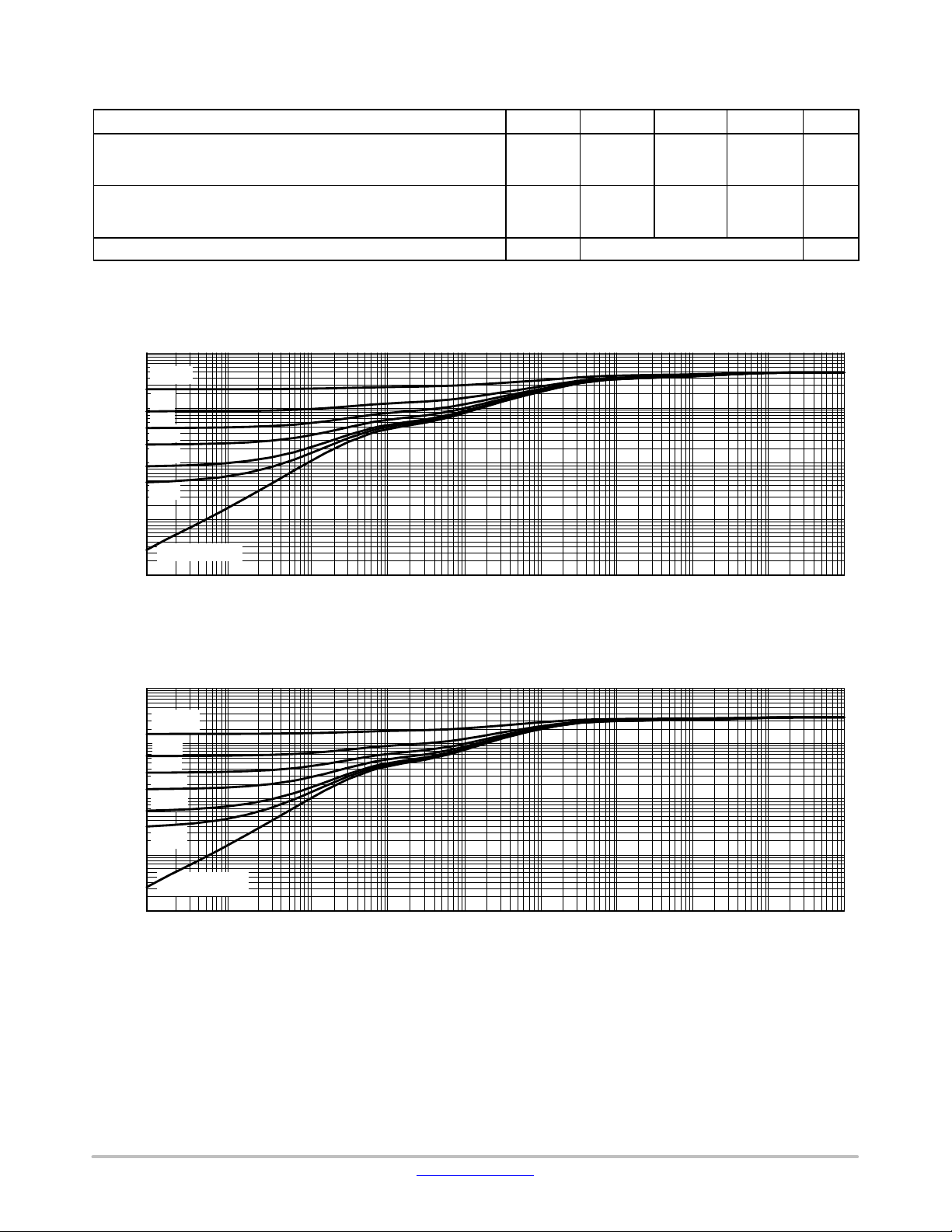
Figure 1. Thermal Response (Note 1)
0.010.001 100.0001 0.10.00001 10.000001
PULSE TIME (sec)
100 1000
100 100
Figure 2. Thermal Response (Note 2)
www.onsemi.com
2
Page 3

NSR05T40XV2
ELECTRICAL CHARACTERISTICS (T
Characteristic
Reverse Leakage
(V
= 10 V)
R
(VR = 40 V)
Forward Voltage
(I
= 10 mA)
F
(IF = 100 mA)
= 200 mA)
(I
F
(I
= 500 mA)
F
Total Capacitance
(V
= 1.0 V, f = 1.0 MHz)
R
Reverse Recovery Time
(I
= IR = 10 mA, I
F
Peak Forward Recovery Voltage
(I
= 100 mA, tr = 20 ns, Figure 4)
F
820 W
+10 V
0.1 mF
50 W OUTPUT
PULSE
GENERATOR
= 1.0 mA, Figure 3)
R(REC)
2.0 k
100 mH
I
F
D.U.T.
= 25°C unless otherwise noted)
A
0.1 mF
50 W INPUT
SAMPLING
V
R
OSCILLOSCOPE
Symbol Min Typ Max Unit
I
R
V
F
C
T
t
rr
V
FRM
t
t
r
p
t
10%
0.5
3.0
360
420
450
530
5.0
55
400
465
525
640
70 pF
20 ns
540 mV
I
F
t
rr
90%
= 1.0 mA
i
R(REC)
OUTPUT PULSE
at i
= 1.0 mA)
R(REC)
INPUT SIGNAL
I
R
= IR = 10 mA; MEASURED
(I
F
mA
mV
t
Notes: 1. A 2.0 kW variable resistor adjusted for a Forward Current (IF) of 10 mA.
Notes: 2. Input pulse is adjusted so I
Notes: 3. t
» t
p
rr
is equal to 10 mA.
R(peak)
Figure 3. Recovery Time Equivalent Test Circuit
I
F
t
r
Time
V
F
V
FRM
V
F
Time
Figure 4. Peak Forward Recovery Voltage Definition
www.onsemi.com
3
Page 4

NSR05T40XV2
TYPICAL CHARACTERISTICS
1000
100
150°C
10
125°C
1
, FORWARD CURRENT (mA)
F
I
75°C
0.1
1000
100
10
1
0.1
10000
1000
150°C
100
125°C
10
75°C
1
0.1
25°C
0.01
25°C
0.2
−25°C
−55°C
0.5
0.7
0.60.40.30.10
0.001
, REVERSE CURRENT (mA)
r
I
0.0001
0.00001
−25°C
−55°C
VF, FORWARD VOLTAGE (V) VR, REVERSE VOLTAGE (V)
Figure 5. Forward Voltage Figure 6. Leakage Current
100
1.0
0.8
0.5
0.2
0.1
10
1
0.1
1.0
0.8
0.5
0.2
0.1
35
40302520151050
0.01
, AVERAGE FORWARD POWER (mW)
F
P
0.001
100
Figure 7. Average Forward Power Dissipation Figure 8. Average Reverse Power Dissipation
100
90
80
70
60
50
40
30
20
, TOTAL CAPACITANCE (pF)
T
C
10
0
0.01
, AVERAGE REVERSE POWER (mW)
R
0.001
250
300200150500 40302520151050
P
500400350 450
IF, FORWARD CURRENT (mA) VR, REVERSE VOLTAGE (V)
25
f = 1.0 MHz
Based on square wave currents
= 25°C prior to surge
T
J
20
15
10
5
, FORWARD SURGE MAX CURRENT (A)
0
25 35
3020151050
V
, REVERSE VOLTAGE (V)
R
Figure 9. Total Capacitance
40
FSM
I
tP, PULSE ON TIME (ms)
Figure 10. Forward Surge Current
35
10001001010.10.010.001
www.onsemi.com
4
Page 5

MECHANICAL CASE OUTLINE
PACKAGE DIMENSIONS
2
1
1
STYLE 1 STYLE 2
SCALE 4:1
b2X
M
0.08 X Y
c
2
−X−
D
−Y−
E
12
TOP VIEW
A
H
E
SIDE VIEW
2X
L
SOD−523
CASE 502−01
ISSUE E
DATE 28 SEP 2010
NOTES:
1. DIMENSIONING AND TOLERANCING PER ASME Y14.5M, 1994.
2. CONTROLLING DIMENSION: MILLIMETERS.
3. MAXIMUM LEAD THICKNESS INCLUDES LEAD FINISH.
MINIMUM LEAD THICKNESS IS THE MINIMUM THICKNESS OF
BASE MATERIAL.
4. DIMENSIONS D AND E DO NOT INCLUDE MOLD FLASH, PROTRUSIONS, OR GATE BURRS.
DIM MIN NOM MAX
A 0.50 0.60 0.70
b 0.25 0.30 0.35
c 0.07 0.14 0.20
D 1.10 1.20 1.30
E 0.70 0.80 0.90
H 1.50 1.60 1.70
L 0.30 REF
L2 0.15 0.20 0.25
MILLIMETERS
E
GENERIC
MARKING DIAGRAM*
XX
M
12
STYLE 1 STYLE 2
XX
M
12
2X
L2
BOTTOM VIEW
RECOMMENDED
SOLDERING FOOTPRINT*
2X
0.48
PACKAGE
OUTLINE
*For additional information on our Pb−Free strategy and soldering
details, please download the ON Semiconductor Soldering and
Mounting Techniques Reference Manual, SOLDERRM/D.
DOCUMENT NUMBER:
DESCRIPTION:
1.80
2X
0.40
DIMENSION: MILLIMETERS
98AON11524D
SOD−523
XX = Specific Device Code
M Date Code
*This information is generic. Please refer to
device data sheet for actual part marking.
Pb−Free indicator, “G” or microdot “ G”,
may or may not be present.
STYLE 1:
PIN 1. CATHODE (POLARITY BAND)
2. ANODE
Electronic versions are uncontrolled except when accessed directly from the Document Repository.
Printed versions are uncontrolled except when stamped “CONTROLLED COPY” in red.
STYLE 2:
NO POLARITY
PAGE 1 OF 1
ON Semiconductor and are trademarks of Semiconductor Components Industries, LLC dba ON Semiconductor or its subsidiaries in the United States and/or other countries.
ON Semiconductor reserves the right to make changes without further notice to any products herein. ON Semiconductor makes no warranty, representation or guarantee regarding
the suitability of its products for any particular purpose, nor does ON Semiconductor assume any liability arising out of the application or use of any product or circuit, and specifically
disclaims any and all liability, including without limitation special, consequential or incidental damages. ON Semiconductor does not convey any license under its patent rights nor the
rights of others.
© Semiconductor Components Industries, LLC, 2019
www.onsemi.com
Page 6

ON Semiconductor and are trademarks of Semiconductor Components Industries, LLC dba ON Semiconductor or its subsidiaries in the United States and/or other countries.
ON Semiconductor owns the rights to a number of patents, trademarks, copyrights, trade secrets, and other intellectual property. A listing of ON Semiconductor ’s product/patent
coverage may be accessed at www.onsemi.com/site/pdf/Patent−Marking.pdf
ON Semiconductor makes no warranty, representation or guarantee regarding the suitability of its products for any particular purpose, nor does ON Semiconductor assume any liability
arising out of the application or use of any product or circuit, and specifically disclaims any and all liability, including without limitation special, consequential or incidental damages.
Buyer is responsible for its products and applications using ON Semiconductor products, including compliance with all laws, regulations and safety requirements or standards,
regardless of any support or applications information provided by ON Semiconductor. “Typical” parameters which may be provided in ON Semiconductor data sheets and/or
specifications can and do vary in different applications and actual performance may vary over time. All operating parameters, including “Typicals” must be validated for each customer
application by customer’s technical experts. ON Semiconductor does not convey any license under its patent rights nor the rights of others. ON Semiconductor products are not
designed, intended, or authorized for use as a critical component in life support systems or any FDA Class 3 medical devices or medical devices with a same or similar classification
in a foreign jurisdiction or any devices intended for implantation in the human body. Should Buyer purchase or use ON Semiconductor products for any such unintended or unauthorized
application, Buyer shall indemnify and hold ON Semiconductor and its officers, employees, subsidiaries, affiliates, and distributors harmless against all claims, costs, damages, and
expenses, and reasonable attorney fees arising out of, directly or indirectly, any claim of personal injury or death associated with such unintended or unauthorized use, even if such
claim alleges that ON Semiconductor was negligent regarding the design or manufacture of the part. ON Semiconductor is an Equal Opportunity/Affirmative Action Employer. This
literature is subject to all applicable copyright laws and is not for resale in any manner.
. ON Semiconductor reserves the right to make changes without further notice to any products herein.
PUBLICATION ORDERING INFORMATION
LITERATURE FULFILLMENT:
Email Requests to: orderlit@onsemi.com
ON Semiconductor Website: www.onsemi.com
TECHNICAL SUPPORT
North American Technical Support:
Voice Mail: 1 800−282−9855 Toll Free USA/Canada
Phone: 011 421 33 790 2910
Europe, Middle East and Africa Technical Support:
Phone: 00421 33 790 2910
For additional information, please contact your local Sales Representative
◊
www.onsemi.com
1
 Loading...