

Page 1
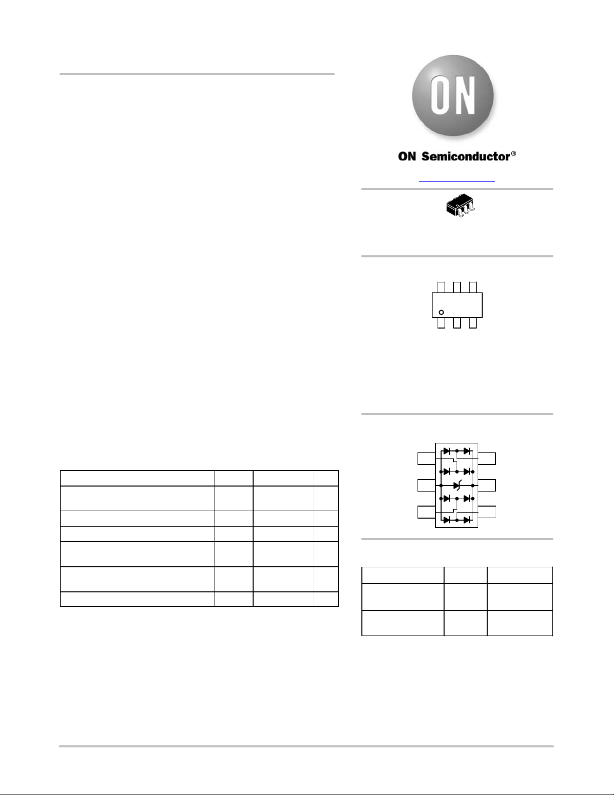
NSP4201MR6
ESD and Surge Protection
Device
Low Clamping Voltage Surge Protection
Diode Array
The NSP4201MR6 surge protector is designed to protect high speed
data lines from ESD, EFT, and lightning surges.
Features
• Protection for the Following IEC Standards:
IEC 61000−4−2 (ESD) ±30 kV (Contact)
IEC 61000−4−5 (Lightning) 25 A (8/20 ms)
• Low Clamping Voltage
• Low Leakage
• UL Flammability Rating of 94 V−0
• SZ Prefix for Automotive and Other Applications Requiring Unique
Site and Control Change Requirements; AEC−Q101 Qualified and
PPAP Capable
• These Devices are Pb−Free, Halogen Free/BFR Free and are RoHS
Compliant
Typical Applications
• High Speed Communication Line Protection
• USB 1.1 and 2.0 Power and Data Line Protection
• Digital Video Interface (DVI)
• Monitors and Flat Panel Displays
MAXIMUM RATINGS (T
Rating
Peak Power Dissipation
8/20 ms @ T
Operating Junction Temperature Range T
Storage Temperature Range T
Lead Solder Temperature −
Maximum (10 Seconds)
IEC 61000−4−2 Air (ESD)
IEC 61000−4−2 Contact (ESD)
IEC 61000−4−4 (5/50 ns) EFT 40 A
Stresses exceeding those listed in the Maximum Ratings table may damage the
device. If any of these limits are exceeded, device functionality should not be
assumed, damage may occur and reliability may be affected.
1. Non−repetitive current pulse per Figure 1 (Pin 5 to Pin 2)
= 25°C (Note 1)
A
See Application Note AND8308/D for further description of
survivability specs.
= 25°C unless otherwise noted)
J
Symbol Value Unit
P
pk
J
stg
T
L
ESD ±30
500 W
−40 to +125 °C
−55 to +150 °C
260 °C
kV
±30
www.onsemi.com
6
1
TSOP−6
CASE 318G
MARKING DIAGRAM
42 MG
G
42 = Specific Device Code
M = Date Code
G = Pb−Free Package
(Note: Microdot may be in either location)
*Date Code orientation may vary
depending upon manufacturing location.
PIN CONFIGURATION AND SCHEMATIC
I/O 1
V
N
I/O 3
2
6 I/O
5 V
4 I/O
P
ORDERING INFORMATION
Device Package Shipping
NSP4201MR6T1G TSOP−6
(Pb−Free)
SZNSP4201MR6T1G TSOP−6
(Pb−Free)
†For information on tape and reel specifications,
including part orientation and tape sizes, please
refer to our Tape and Reel Packaging Specification
Brochure, BRD8011/D.
3000 / Tape &
Reel
3000 / Tape &
Reel
© Semiconductor Components Industries, LLC, 2017
June, 2017 − Rev. 1
1 Publication Order Number:
NSP4201MR6/D
Page 2
NSP4201MR6
ELECTRICAL CHARACTERISTICS
(TA = 25°C unless otherwise noted)
Symbol Parameter
I
V
V
RWM
V
V
P
*See Application Note AND8308/D for detailed explanations of
datasheet parameters.
ELECTRICAL CHARACTERISTICS (T
Reverse Working Voltage V
Breakdown Voltage V
Reverse Leakage Current I
Clamping Voltage
= 8/20 ms per Figure 1)
(t
p
Junction Capacitance C
Junction Capacitance C
2. Surge protection devices are normally selected according to the working peak reverse voltage (V
than the DC or continuous peak operating voltage level.
3. V
Maximum Reverse Peak Pulse Current
PP
Clamping Voltage @ I
C
PP
Working Peak Reverse Voltage
I
Maximum Reverse Leakage Current @ V
R
Breakdown Voltage @ I
BR
I
Test Current
T
I
Forward Current
F
Forward Voltage @ I
F
Peak Power Dissipation
pk
T
F
C Capacitance @ VR = 0 and f = 1.0 MHz
=25°C unless otherwise specified)
J
Parameter
Symbol Conditions Min Typ Max Unit
RWM
V
(Note 2) 5.0 V
IT=1 mA, (Note 3) 6.0 V
BR
V
R
C
RWM
IPP = 1 A, Any I/O to GND 8.5
IPP = 5 A, Any I/O to GND 9.0
IPP = 8 A, Any I/O to GND 10
IPP = 25 A, Any I/O to GND 12
VR = 0 V, f=1 MHz between I/O Pins and GND 3.0 5.0 pF
J
VR = 0 V, f=1 MHz between I/O Pins 1.5 3.0 pF
J
is measured at pulse test current IT.
BR
V
VCV
RWM
BR
RWM
Uni−Directional Surge Protection
= 5 V 1.0
I
I
F
I
V
R
F
I
T
I
PP
), which should be equal or greater
RWM
V
mA
V
100
90
80
70
60
50
t
r
PEAK VALUE I
HALF VALUE I
@ 8 ms
RSM
PULSE WIDTH (tP) IS DEFINED
AS THAT POINT WHERE THE
PEAK CURRENT DECAY = 8 ms
/2 @ 20 ms
RSM
40
30
20
% OF PEAK PULSE CURRENT
10
0
t
P
020406080
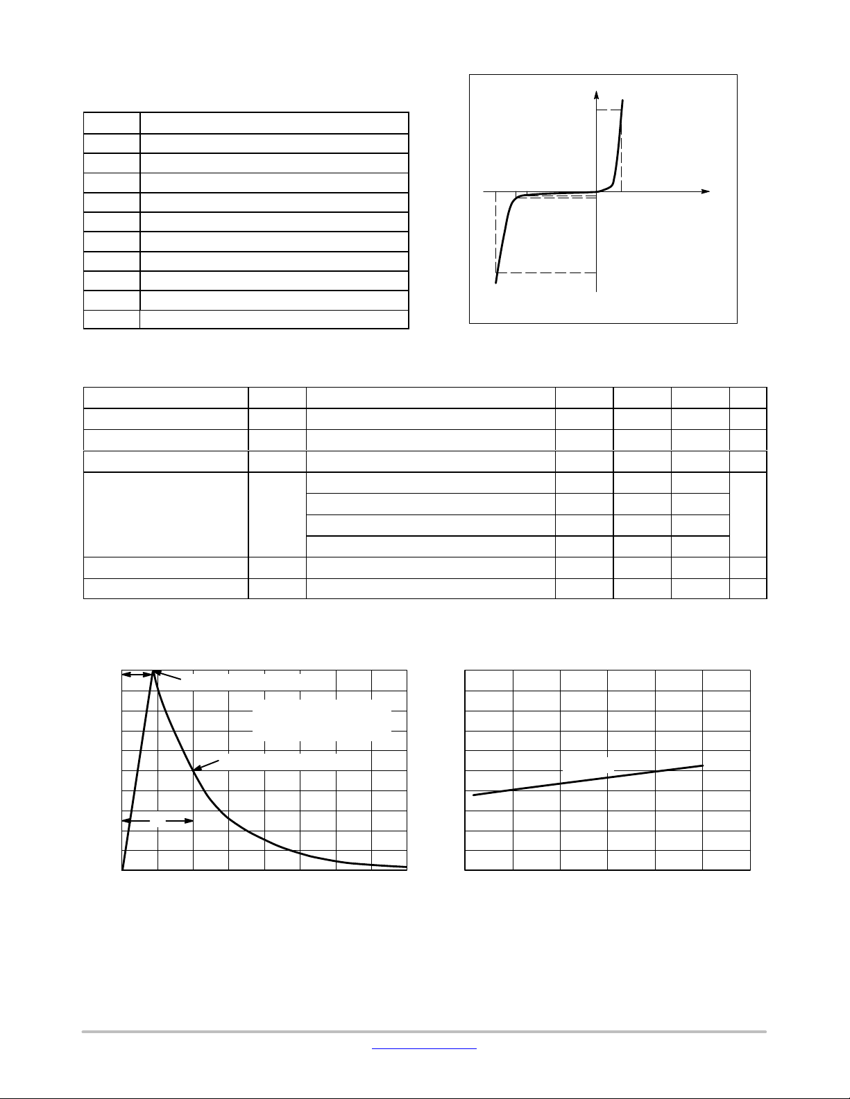
t, TIME (ms)
Figure 1. IEC61000−4−5 8/20 ms Pulse Waveform
www.onsemi.com
20
18
16
14
12
10
I/O−GND
8
6
4
CLAMPING VOLTAGE (V)
2
0
05
10 15 20 25
PEAK PULSE CURRENT (A)
Figure 2. Clamping Voltage vs. Peak Pulse Current
(t
= 8/20 ms per Figure 1)
p
2
30
Page 3
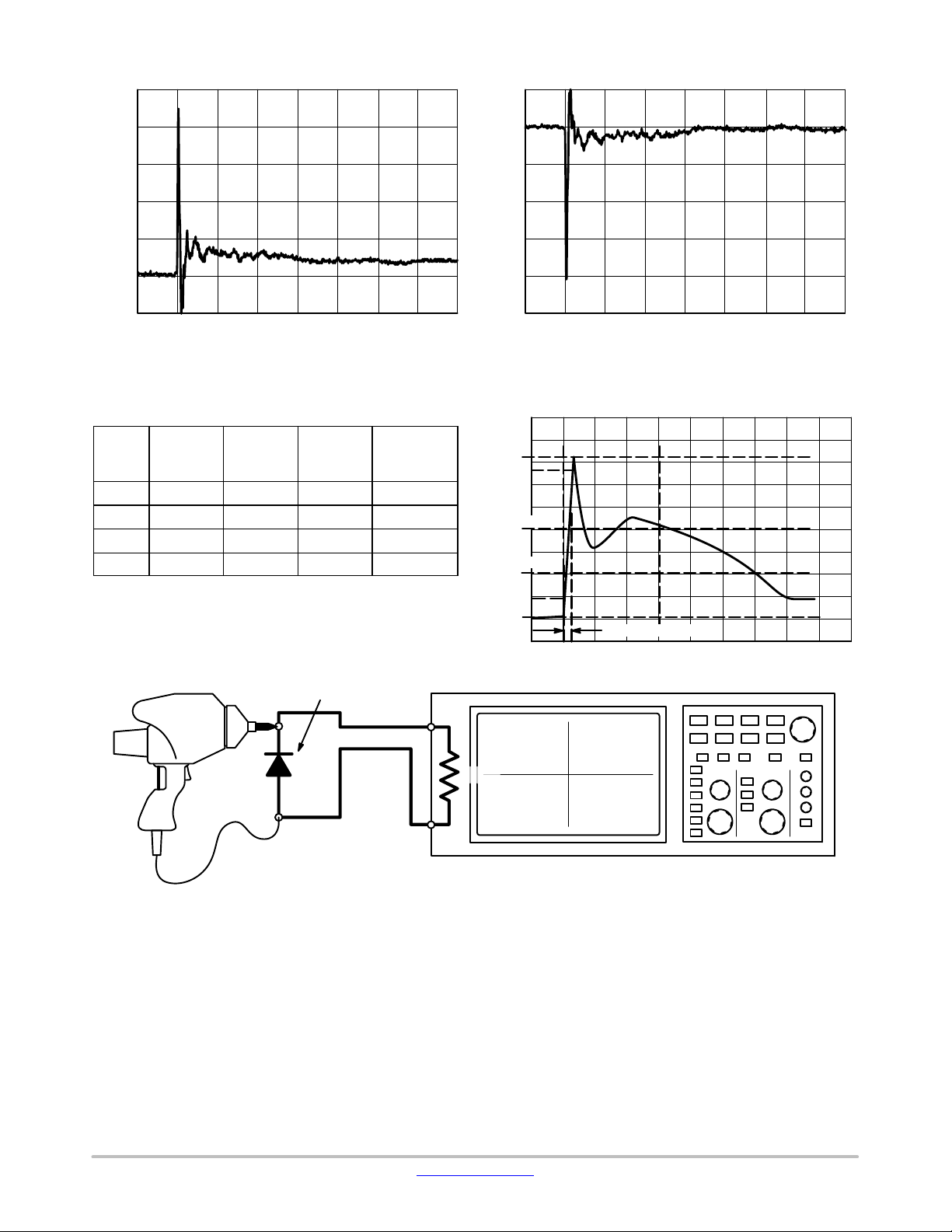
NSP4201MR6
100
80
60
40
VOLTAGE (V)
20
0
−20
−20 0 20 40 60 80 100 120 140
TIME (ns)
Figure 3. IEC61000−4−2 +8 kV Contact Clamping
Voltage
IEC 61000−4−2 Spec.
Test Volt-
Level
age (kV)
1 2 7.5 4 2
2 4 15 8 4
3 6 22.5 12 6
4 8 30 16 8
First Peak
Current
(A)
Current at
30 ns (A)
Current at
60 ns (A)
20
0
−20
−40
VOLTAGE (V)
−60
−80
−100
−20 0 20 40 60 80 100 120 140
TIME (ns)
Figure 4. IEC61000−4−2 −8 kV Contact Clamping
Voltage
IEC61000−4−2 Waveform
I
peak
100%
90%
I @ 30 ns
I @ 60 ns
Figure 5. IEC61000−4−2 Spec
ESD Gun
Surge Protection
Oscilloscope
50 W
Cable
Figure 6. Diagram of ESD Test Setup
The following is taken from Application Note
AND8308/D − Interpretation of Datasheet Parameters
for ESD Devices.
ESD Voltage Clamping
For sensitive circuit elements it is important to limit the
voltage that an IC will be exposed to during an ESD event
to as low a voltage as possible. The ESD clamping voltage
is the voltage drop across the ESD protection diode during
an ESD event per the IEC61000−4−2 waveform. Since the
IEC61000−4−2 was written as a pass/fail spec for larger
10%
tP = 0.7 ns to 1 ns
50 W
systems such as cell phones or laptop computers it is not
clearly defined in the spec how to specify a clamping voltage
at the device level. ON Semiconductor has developed a way
to examine the entire voltage waveform across the ESD
protection diode over the time domain of an ESD pulse in the
form of an oscilloscope screenshot, which can be found on
the datasheets for all ESD protection diodes. For more
information on how ON Semiconductor creates these
screenshots and how to interpret them please refer to
AND8307/D.
www.onsemi.com
3
Page 4

TYPICAL PERFORMANCE CURVES
5.0
5
PEAK POWER DISSIPATION (%)
(TJ = 25°C unless otherwise noted)
100
90
80
70
60
50
40
30
20
10
0
0 25 50 75 100 125 150 175 200
T
, AMBIENT TEMPERATURE (°C)
A
Figure 7. Pulse Derating Curve
NSP4201MR6
4.5
4.0
3.5
3.0
2.5
2.0
1.5
1.0
JUNCTION CAPACITANCE (pF)
0.5
0.0
01
Figure 8. Junction Capacitance vs Reverse Voltage
I/O−GND
I/O−I/O
234
, REVERSE VOLTAGE (V)
V
BR
Figure 9. RF Insertion Loss
www.onsemi.com
4
Page 5

NSP4201MR6
TYPICAL APPLICATIONS
RJ45
Connector
PHY
Ethernet
(10/100)
TX+
TX−
RX+
RX−
V
CC
GND
Coupling
Transformers
NSP4201MR6
N/C N/C
Figure 10. Protection for Ethernet 10/100 (Differential mode)
R1
RTIP
R3
RRING
V
CC
R2
TX+
TX−
RX+
RX−
T1
T1/E1
TRANCEIVER
TTIP
TRING
NSP4201MR6
R4
R5
T2
Figure 11. TI/E1 Interface Protection
www.onsemi.com
5
Page 6

MECHANICAL CASE OUTLINE
PACKAGE DIMENSIONS
1
SCALE 2:1
D
456
E1
NOTE 5
0.05
A1
23
1
e
E
b
A
DETAIL Z
c
CASE 318G−02
H
L
M
DETAIL Z
TSOP−6
ISSUE V
L2
GAUGE
PLANE
SEATING
C
PLANE
DATE 12 JUN 2012
NOTES:
1. DIMENSIONING AND TOLERANCING PER ASME Y14.5M, 1994.
2. CONTROLLING DIMENSION: MILLIMETERS.
3. MAXIMUM LEAD THICKNESS INCLUDES LEAD FINISH. MINIMUM
LEAD THICKNESS IS THE MINIMUM THICKNESS OF BASE MATERIAL.
4. DIMENSIONS D AND E1 DO NOT INCLUDE MOLD FLASH,
PROTRUSIONS, OR GATE BURRS. MOLD FLASH, PROTRUSIONS, OR
GATE BURRS SHALL NOT EXCEED 0.15 PER SIDE. DIMENSIONS D
AND E1 ARE DETERMINED AT DATUM H.
5. PIN ONE INDICATOR MUST BE LOCATED IN THE INDICATED ZONE.
DIMAMIN NOM MAX
A1 0.01 0.06 0.10
b 0.25 0.38 0.50
c 0.10 0.18 0.26
D 2.90 3.00 3.10
E 2.50 2.75 3.00
E1
e 0.85 0.95 1.05
L 0.20 0.40 0.60
L2
M
MILLIMETERS
0.90 1.00 1.10
1.30 1.50 1.70
0.25 BSC
0° 10°
−
STYLE 1:
PIN 1. DRAIN
2. DRAIN
3. GATE
4. SOURCE
5. DRAIN
6. DRAIN
STYLE 7:
PIN 1. COLLECTOR
2. COLLECTOR
3. BASE
4. N/C
5. COLLECTOR
6. EMITTER
STYLE 13:
PIN 1. GATE 1
2. SOURCE 2
3. GATE 2
4. DRAIN 2
5. SOURCE 1
6. DRAIN 1
STYLE 2:
PIN 1. EMITTER 2
2. BASE 1
3. COLLECTOR 1
4. EMITTER 1
5. BASE 2
6. COLLECTOR 2
STYLE 8:
PIN 1. Vbus
2. D(in)
3. D(in)+
4. D(out)+
5. D(out)
6. GND
STYLE 14:
PIN 1. ANODE
2. SOURCE
3. GATE
4. CATHODE/DRAIN
5. CATHODE/DRAIN
6. CATHODE/DRAIN
STYLE 3:
PIN 1. ENABLE
2. N/C
3. R BOOST
4. Vz
5. V in
6. V out
STYLE 9:
PIN 1. LOW VOLTAGE GATE
2. DRAIN
3. SOURCE
4. DRAIN
5. DRAIN
6. HIGH VOLTAGE GATE
STYLE 15:
PIN 1. ANODE
2. SOURCE
3. GATE
4. DRAIN
5. N/C
6. CATHODE
RECOMMENDED
SOLDERING FOOTPRINT*
6X
0.60
3.20
DIMENSIONS: MILLIMETERS
*For additional information on our Pb−Free strategy and soldering
details, please download the ON Semiconductor Soldering and
Mounting Techniques Reference Manual, SOLDERRM/D.
DOCUMENT NUMBER:
DESCRIPTION:
98ASB14888C
TSOP−6
6X
0.95
0.95
PITCH
STYLE 4:
PIN 1. N/C
2. V in
3. NOT USED
4. GROUND
5. ENABLE
6. LOAD
STYLE 10:
PIN 1. D(OUT)+
2. GND
3. D(OUT)−
4. D(IN)−
5. VBUS
6. D(IN)+
STYLE 16:
PIN 1. ANODE/CATHODE
2. BASE
3. EMITTER
4. COLLECTOR
5. ANODE
6. CATHODE
STYLE 5:
PIN 1. EMITTER 2
2. BASE 2
3. COLLECTOR 1
4. EMITTER 1
5. BASE 1
6. COLLECTOR 2
STYLE 11:
PIN 1. SOURCE 1
2. DRAIN 2
3. DRAIN 2
4. SOURCE 2
5. GATE 1
6. DRAIN 1/GATE 2
STYLE 17:
PIN 1. EMITTER
2. BASE
3. ANODE/CATHODE
4. ANODE
5. CATHODE
6. COLLECTOR
STYLE 6:
PIN 1. COLLECTOR
2. COLLECTOR
3. BASE
4. EMITTER
5. COLLECTOR
6. COLLECTOR
STYLE 12:
PIN 1. I/O
2. GROUND
3. I/O
4. I/O
5. VCC
6. I/O
GENERIC
MARKING DIAGRAM*
XXXAYWG
G
1
XXX = Specific Device Code
A =Assembly Location
Y = Year
XXX = Specific Device Code
M = Date Code
G = Pb−Free Package
W = Work Week
G = Pb−Free Package
*This information is generic. Please refer to device data sheet
for actual part marking. Pb−Free indicator, “G” or microdot “
G”, may or may not be present.
Electronic versions are uncontrolled except when accessed directly from the Document Repository.
Printed versions are uncontrolled except when stamped “CONTROLLED COPY” in red.
XXX MG
G
1
STANDARDIC
PAGE 1 OF 1
ON Semiconductor and are trademarks of Semiconductor Components Industries, LLC dba ON Semiconductor or its subsidiaries in the United States and/or other countries.
ON Semiconductor reserves the right to make changes without further notice to any products herein. ON Semiconductor makes no warranty, representation or guarantee regarding
the suitability of its products for any particular purpose, nor does ON Semiconductor assume any liability arising out of the application or use of any product or circuit, and specifically
disclaims any and all liability, including without limitation special, consequential or incidental damages. ON Semiconductor does not convey any license under its patent rights nor the
rights of others.
© Semiconductor Components Industries, LLC, 2019
www.onsemi.com
Page 7

ON Semiconductor and are trademarks of Semiconductor Components Industries, LLC dba ON Semiconductor or its subsidiaries in the United States and/or other countries.
ON Semiconductor owns the rights to a number of patents, trademarks, copyrights, trade secrets, and other intellectual property. A listing of ON Semiconductor’s product/patent
coverage may be accessed at www.onsemi.com/site/pdf/Patent−Marking.pdf
ON Semiconductor makes no warranty, representation or guarantee regarding the suitability of its products for any particular purpose, nor does ON Semiconductor assume any liability
arising out of the application or use of any product or circuit, and specifically disclaims any and all liability, including without limitation special, consequential or incidental damages.
Buyer is responsible for its products and applications using ON Semiconductor products, including compliance with all laws, regulations and safety requirements or standards,
regardless of any support or applications information provided by ON Semiconductor. “Typical” parameters which may be provided in ON Semiconductor data sheets and/or
specifications can and do vary in different applications and actual performance may vary over time. All operating parameters, including “Typicals” must be validated for each customer
application by customer’s technical experts. ON Semiconductor does not convey any license under its patent rights nor the rights of others. ON Semiconductor products are not
designed, intended, or authorized for use as a critical component in life support systems or any FDA Class 3 medical devices or medical devices with a same or similar classification
in a foreign jurisdiction or any devices intended for implantation in the human body. Should Buyer purchase or use ON Semiconductor products for any such unintended or unauthorized
application, Buyer shall indemnify and hold ON Semiconductor and its officers, employees, subsidiaries, affiliates, and distributors harmless against all claims, costs, damages, and
expenses, and reasonable attorney fees arising out of, directly or indirectly, any claim of personal injury or death associated with such unintended or unauthorized use, even if such
claim alleges that ON Semiconductor was negligent regarding the design or manufacture of the part. ON Semiconductor is an Equal Opportunity/Affirmative Action Employer. This
literature is subject to all applicable copyright laws and is not for resale in any manner.
. ON Semiconductor reserves the right to make changes without further notice to any products herein.
PUBLICATION ORDERING INFORMATION
LITERATURE FULFILLMENT:
Email Requests to: orderlit@onsemi.com
ON Semiconductor Website: www.onsemi.com
TECHNICAL SUPPORT
North American Technical Support:
Voice Mail: 1 800−282−9855 Toll Free USA/Canada
Phone: 011 421 33 790 2910
Europe, Middle East and Africa Technical Support:
Phone: 00421 33 790 2910
For additional information, please contact your local Sales Representative
◊
www.onsemi.com
1
 Loading...