

Page 1
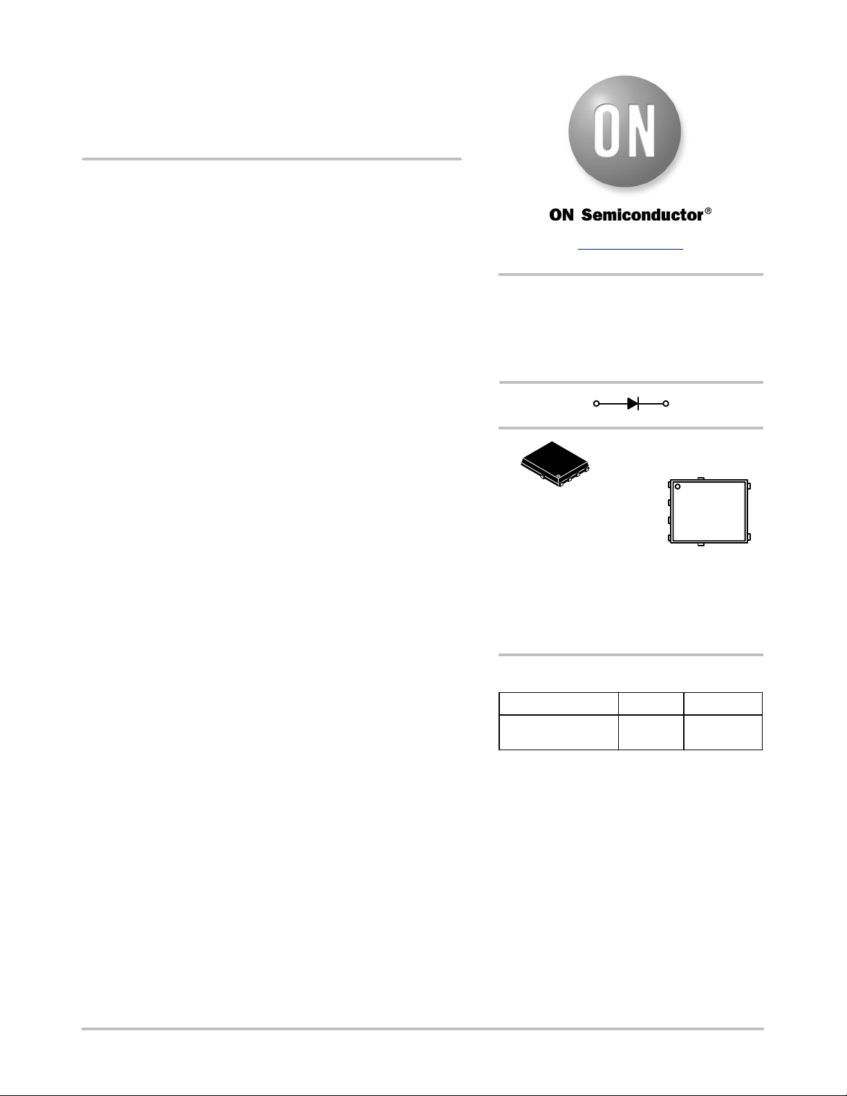
Schottky Barrier Rectifier
Trench-based, High
Performance
NRTS3060MFS
This Trench Schottky rectifier is high performance device in SO−8
FL package. The lower forward voltage, less leakage current, and
small junction capacitance are suitable to high switching frequency
high density DC to DC conversion application. Offering higher
avalanche energy capability for Oring or reverse protection
application. The SO−8 FL package provides an excellent thermal
performance, less land area of board space, and low profile.
Features
• Lower Forward Voltage Drop
• Less Leakage Current in High Temperature
• Small Junction Capacitance for High Switching Frequency
• Higher Avalanche Energy Capability
• 175°C Operating Junction Temperature
• Good Alternative Solution of SMC and DPAK Package
• Small Footprint − Land Area: 31.2 mm
• Low Profile − Maximum Height of 1.1 mm
• These Devices are Pb−Free, Halogen Free/BFR Free and are RoHS
Compliant
2
www.onsemi.com
TRENCH SCHOTTKY
RECTIFIER
30 AMPERES
60 VOLTS
1,2,3
1
SO−8 FLAT LEAD
CASE 488AA
STYLE 2
Not Used
5,6
MARKING
DIAGRAM
A
A
A
C
T3060
AYWZZ
C
Mechanical Characteristics:
• Case: Molded Epoxy
• Epoxy Meets UL 94 V−0 @ 0.125 in
• Weight: 95 mg (Approximately)
• Lead and Mounting Surface Temperature for Soldering Purposes:
260°C Maximum for 10 Seconds
• MSL 1
Applications
• High Switching Frequency DC/DC Converter
nd
• 2
Rectifier
• Freewheeling Diode used with Inductive Load
• Oring / Reverse Protection
T3060 = Specific Device Code
A = Assembly Location
Y = Year
W = Work Week
ZZ = Lot Traceability
ORDERING INFORMATION
Device Package Shipping
NRTS3060MFST3G SO−8 FL
(Pb−Free)
†For information on tape and reel specifications,
including part orientation and tape sizes, please
refer to our Tape and Reel Packaging Specification
Brochure, BRD8011/D.
5000 /
Tape & Reel
†
© Semiconductor Components Industries, LLC, 2021
January, 2021 − Rev. 0
1 Publication Order Number:
NRTS3060MFS/D
Page 2
NRTS3060MFS
MAXIMUM RATINGS
Rating Symbol Value Unit
Peak Repetitive Reverse Voltage
Working Peak Reverse Voltage
DC Blocking Voltage
Continuous Forward Current (TC = 164°C, DC) I
Peak Repetitive Forward Current (TC = 162°C, Square Wave, Duty = 0.5) I
Non−Repetitive Peak Surge Current
Sinusoidal Halfwave, 8.3 ms
Square wave, 1 ms 600
Square wave, 100 ms
Non−Repetitive Avalanche Energy (TJ = 25°C) E
Storage Temperature Range T
Operating Junction Temperature Range (Note 1) T
ESD Rating (Human Body Model) 3B
ESD Rating (Machine Model) M4
Stresses exceeding those listed in the Maximum Ratings table may damage the device. If any of these limits are exceeded, device functionality
should not be assumed, damage may occur and reliability may be affected.
1. The heat generated must be less than the thermal conductivity from Junction−to−Ambient dP
V
RRM
V
RWM
V
R
F(DC)
FRM
I
FSM
AS
stg
J
/dTJ < 1/R
D
60 V
30 A
60 A
350
1200
800 mJ
−65 to +175 °C
−55 to +175 °C
q
JA
A
THERMAL CHARACTERISTICS
Characteristic Symbol Max Unit
Thermal Resistance, Junction−to−Ambient (Note 2)
Thermal Resistance, Junction−to−Case Bottom (Note 2)
Thermal Characterization, Junction−to−Case Top (Note 2)
Thermal Characterization, Junction−to−Lead of Cathode (Note 2)
R
q
JA
R
q
JCB
y
JCT
y
JLC
56 °C/W
0.65 °C/W
3.72 °C/W
1.44 °C/W
2. Assume 600 mm2, 1 oz. copper bond pad on a FR4 board.
ELECTRICAL CHARACTERISTICS
Characteristic Symbol Typ Max Unit
Instantaneous Forward Voltage
= 15 A, TJ = 25°C)
(I
F
(I
= 15 A, TJ = 125°C)
F
(I
= 30 A, TJ = 25°C)
F
(I
= 30 A, TJ = 125°C)
F
Instantaneous Reverse Current
= Rated DC Voltage, TJ = 25°C)
(V
R
(V
= Rated DC Voltage, TJ = 125°C)
R
Junction Capacitance
= 1 V, TJ = 25°C, f = 1 MHz)
(V
R
Product parametric performance is indicated in the Electrical Characteristics for the listed test conditions, unless otherwise noted. Product
performance may not be indicated by the Electrical Characteristics if operated under different conditions.
3. Pulse Test: Pulse Width = 300 ms, Duty Cycle ≤ 2.0%.
V
F
I
R
C
J
0.48
0.40
0.53
0.48
17
10
−
−
0.60
0.57
100
30
V
mA
mA
pF
3140 −
www.onsemi.com
2
Page 3

NRTS3060MFS
TYPICAL CHARACTERISTICS
120
110
100
90
80
70
60
50
40
30
20
, PEAK FORWARD CURRENT (A)
10
F(PK)
I
0
40
25
55 70 85 115 145130 160
Figure 1. Forward Current Derating of Case
100
TA = 150°C
10
CURRENT (A)
1
, INSTANTANEOUS FORWARD
F
I
0.1
0.1 0.5 0.9 0.3 0.5 0.9
VF, INSTANTANEOUS FORWARD VOLTAGE (V) VF, INSTANTANEOUS FORWARD VOLTAGE (V)
Figure 3. Typical Forward Characteristics Figure 4. Maximum Forward Characteristics
TJ = 175°C
R
q
JCB
Square Wave (Duty = 0.5)
100 175
TC, CASE TEMPERATURE (°C)
Temperature
TA = 175°C
TA = 125°C
TA = 85°C
TA = 25°C
TA = −20°C
TA = −40°C
0.70.60.40.30.20
30
11510070554025
TJ = 175°C
R
= 56°C/W
q
JA
Square Wave
145 160 175
= 0.65°C/W
DC
D = 0.2
25
D = 0.3
20
15
D = 0.5
10
DC
5
, PEAK FORWARD CURRENT (A)
F(PK)
I
0
85 130
TA, AMBIENT TEMPERATURE (°C)
Figure 2. Forward Current Derating of Ambient
Temperature
100
10
CURRENT (A)
1
, INSTANTANEOUS FORWARD
F
I
0.1
0.8 0.6 1.0
1.0
TA = 25°C
TA = 125°C
TA = −40°C
0.80.70.40.20.10
1.E+00
1.E−01
TA = 175°C
TA = 150°C
1.E−02
1.E−03
1.E−04
1.E−05
TA = 125°C
TA = 85°C
TA = 25°C
1.E−06
1.E−07
TA = −20°C
1.E−08
1.E−09
TA = −40°C
1.E−10
1.E−11
, INSTANTANEOUS REVERSE CURRENT (A)
R
I
VR, INSTANTANEOUS REVERSE VOLTAGE (V) VR, INSTANTANEOUS REVERSE VOLTAGE (V)
Figure 5. Typical Reverse Characteristics Figure 6. Maximum Reverse Characteristics
1.E−00
1.E−01
1.E−02
1.E−03
1.E−04
1.E−05
1.E−06
1.E−07
1.E−08
1.E−09
1.E−10
1.E−11
, INSTANTANEOUS REVERSE CURRENT (A)
6050403020100
R
I
www.onsemi.com
3
TA = 125°C
TA = 25°C
TA = −40°C
6050403020100
Page 4

NRTS3060MFS
TYPICAL CHARACTERISTICS
10,000
1000
100
C, JUNCTION CAPACITANCE (pF)
10
0.1
100
10
1
R(t) (C/W)
0.1
1
VR, REVERSE VOLTAGE (V)
10 100
Figure 7. Typical Junction Capacitance
50% (DUTY CYCLE)
20%
10%
5.0%
2.0%
1.0%
TJ = 25°C
, AVERAGE FORWARD
POWER DISSIPATION (A)
F(AV)
P
25
TJ = 175°C
Square Wave
20
D = 0.3
15
D = 0.2
10
5
0
I
, AVERAGE FORWARD CURRENT (A)
F(AV)
151050
20
Figure 8. Average Forward Power Dissipation
D = 0.5
DC
25 30
0.01
0.001
SINGLE PULSE
(Assumes 600 mm2, 1 oz. copper bond pad on a FR4 board)
0.0001 0.001 0.01 1
PULSE TIME (s)
0.10.00001
Figure 9. Typical Thermal Characteristics, Junction−to−Ambient
10 1000.000001
1000
www.onsemi.com
4
Page 5

0.05
0.10 C
0.10 C
C
c
D
2
D1
1234
TOP VIEW
SIDE VIEW
8X
b
A0.10 B
L
14
2 X
e/2
e
0.20 C
A
E1
E
2
A
DETAIL A
K
NRTS3060MFS
PACKAGE DIMENSIONS
DFN5 5x6, 1.27P
(SO−8FL)
CASE 488AA
ISSUE N
B
2 X
0.20 C
c
DETAIL A
2X
2X
0.475
NOTES:
4 X
q
A1
C
SEATING
PLANE
RECOMMENDED
SOLDERING FOOTPRINT*
4.5600.495
2X
1.530
1. DIMENSIONING AND TOLERANCING PER
ASME Y14.5M, 1994.
2. CONTROLLING DIMENSION: MILLIMETER.
3. DIMENSION D1 AND E1 DO NOT INCLUDE
MOLD FLASH PROTRUSIONS OR GATE
BURRS.
DIM MIN NOM
A1 0.00 −−−
D1 4.70 4.90
D2 3.80 4.00
E1 5.70 5.90
E2 3.45 3.65
L1 0.125 REF
MILLIMETERS
A 0.90 1.00
b 0.33 0.41
c 0.23 0.28
5.00 5.30
D 5.15
E 6.15
6.00 6.30
e 1.27 BSC
G 0.51 0.575
K 1.20 1.35
L 0.51 0.575
M 3.00 3.40
q 0 −−−
_
STYLE 1:
PIN 1. SOURCE
2. SOURCE
3. SOURCE
4. GATE
5. DRAIN
MAX
1.10
0.05
0.51
0.33
5.10
4.20
6.10
3.85
0.71
1.50
0.71
3.80
12
_
3.200
4.530
1.330
PIN 5
(EXPOSED PAD)
E2
L1
2X
M
0.905
1
0.965
G
BOTTOM VIEW
D2
1.000
4X
4X
0.750
1.270
PITCH
DIMENSIONS: MILLIMETERS
*For additional information on our Pb−Free strategy and soldering
details, please download the ON Semiconductor Soldering and
Mounting Techniques Reference Manual, SOLDERRM/D.
ON Semiconductor and are trademarks of Semiconductor Components Industries, LLC dba ON Semiconductor or its subsidiaries in the United States and/or other countries.
ON Semiconductor owns the rights to a number of patents, trademarks, copyrights, trade secrets, and other intellectual property. A listing of ON Semiconductor’s product/patent
coverage may be accessed at www.onsemi.com/site/pdf/Patent−Marking.pdf
ON Semiconductor makes no warranty, representation or guarantee regarding the suitability of its products for any particular purpose, nor does ON Semiconductor assume any liability
arising out of the application or use of any product or circuit, and specifically disclaims any and all liability, including without limitation special, consequential or incidental damages.
Buyer is responsible for its products and applications using ON Semiconductor products, including compliance with all laws, regulations and safety requirements or standards,
regardless of any support or applications information provided by ON Semiconductor. “Typical” parameters which may be provided in ON Semiconductor data sheets and/or
specifications can and do vary in different applications and actual performance may vary over time. All operating parameters, including “Typicals” must be validated for each customer
application by customer’s technical experts. ON Semiconductor does not convey any license under its patent rights nor the rights of others. ON Semiconductor products are not
designed, intended, or authorized for use as a critical component in life support systems or any FDA Class 3 medical devices or medical devices with a same or similar classification
in a foreign jurisdiction or any devices intended for implantation in the human body. Should Buyer purchase or use ON Semiconductor products for any such unintended or unauthorized
application, Buyer shall indemnify and hold ON Semiconductor and its officers, employees, subsidiaries, affiliates, and distributors harmless against all claims, costs, damages, and
expenses, and reasonable attorney fees arising out of, directly or indirectly, any claim of personal injury or death associated with such unintended or unauthorized use, even if such
claim alleges that ON Semiconductor was negligent regarding the design or manufacture of the part. ON Semiconductor is an Equal Opportunity/Affirmative Action Employer. This
literature is subject to all applicable copyright laws and is not for resale in any manner.
. ON Semiconductor reserves the right to make changes without further notice to any products herein.
PUBLICATION ORDERING INFORMATION
LITERATURE FULFILLMENT:
Email Requests to: orderlit@onsemi.com
ON Semiconductor Website: www.onsemi.com
TECHNICAL SUPPORT
North American Technical Support:
Voice Mail: 1 800−282−9855 Toll Free USA/Canada
Phone: 011 421 33 790 2910
Europe, Middle East and Africa Technical Support:
Phone: 00421 33 790 2910
For additional information, please contact your local Sales Representative
◊
www.onsemi.com
5
 Loading...