

Page 1
4-Bit 100 Mb/s Configurable
Dual-Supply Level
Translator
NLSX5004, NLSXN5004
The NLSX5004 and NLSXN5004 are 4−bit configurable
dual−supply autosensing bidirectional level translators that do not
require direction control pins. The A− and B−ports are designed to
track two different power supply rails, V
Both the V
and the V
CCA
supply rails are independently−
CCB
configurable from 0.9 V to 3.6 V.
The NLSX5004 and NLSXN5004 have high dynamic output
current capability, allowing the translators to drive high capacitive
loads.
Enable input pins are available to reduce the power consumption.
These pins may be used to disable both A− and B−ports by putting
them in 3−state significantly reducing the supply current from both
V
CCA
and V
. These pins are referenced to the V
CCB
NLSX5004 has an active−High enable (EN) while the NLSXN5004
has active−Low enable (EN).
Features
• Wide V
• V
CCA
− V
, V
CCA
and V
may be greater than, equal to, or less than V
CCA
Operating Range: 0.9 V to 3.6 V
CCB
are independent
CCB
• High 100 pF Capacitive Drive Capability
• High−Speed w/ 140 Mbps Guaranteed Date Rate for V
V
> 1.8 V
CCB
• Low Bit−to−Bit skew
• Overvoltage Tolerant Enable and I/O Pins
• Non−preferential Power−Up Sequencing
• Partial Power−Off Protection
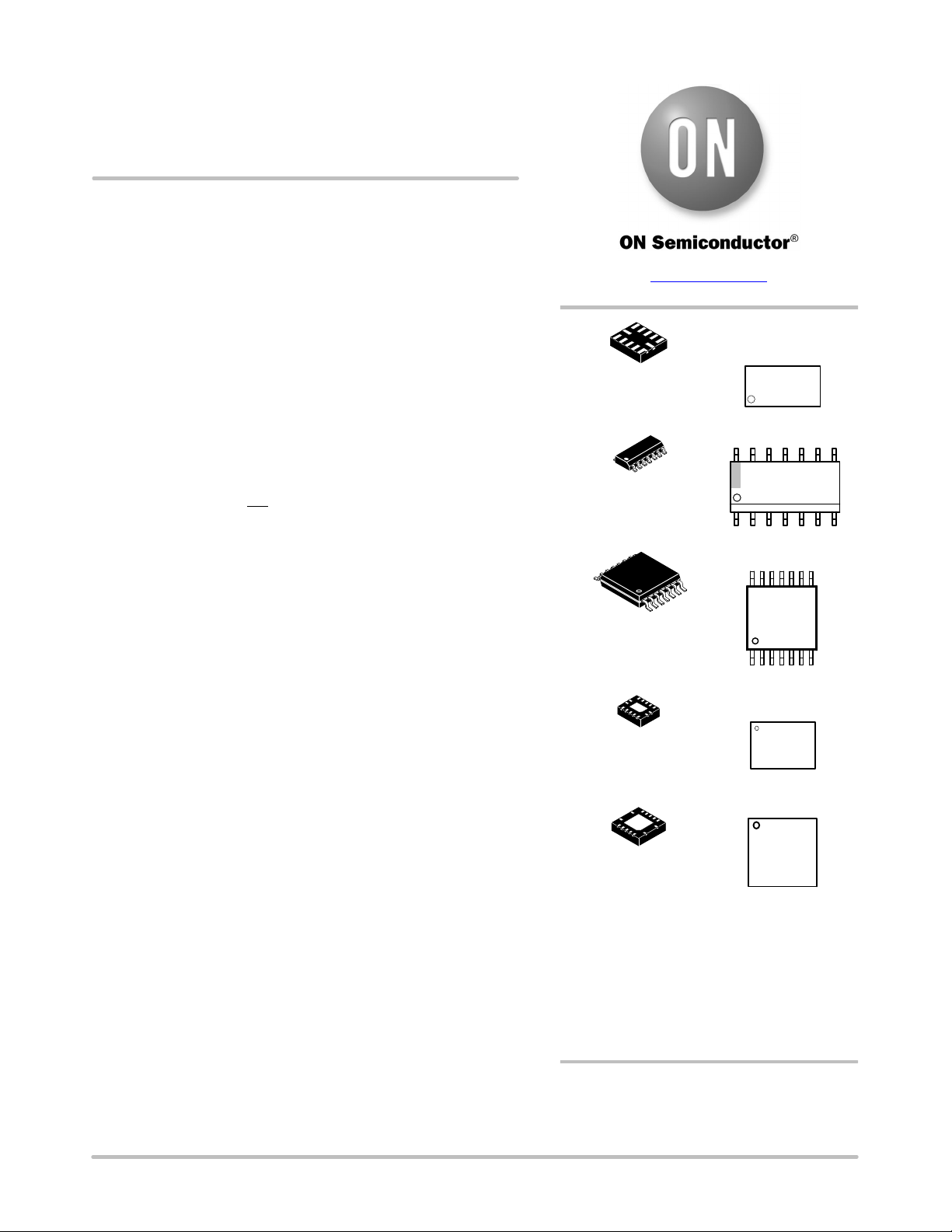
• Available packaging:
UQFN−12, SOIC14, TSSOP14, QFN−14, Other packages
• NLV Prefix for Automotive and Other Applications Requiring
Unique Site and Control Change Requirements; AEC−Q100
Qualified and PPAP Capable
• These Devices are Pb−Free, Halogen Free/BFR Free and RoHS
Compliant
Typical Applications
• Mobile Phones, Infotainment Systems, Other Devices
Important Information
• ESD Protection for All Pins:
HBM (Human Body Model) − 2000 V
CCA
and V
respectively.
CCB
supply. The
CCA
CCB
CCA
,
www.onsemi.com
MARKING
DIAGRAMS
1
UQFN12
MU SUFFIX
CASE 523AE
14
1
SOIC14
D SUFFIX
CASE 751A
14
1
TSSOP14
DT SUFFIX
CASE 948G
1
QFN14
MN SUFFIX
CASE 485DE
QFN14
MN SUFFIX
CASE 485AL
XXXXX = Specific Device Code
M = Date Code
A = Assembly Location
L or WL = Wafer Lot
Y = Year
W or WW = Work Week
G or G = Pb−Free Package
(Note: Microdot may be in either location)
14
A2M
XXXXXXXXXG
AWLYWW
1
14
XXXX
XXXX
ALYWG
1
XXXX
AYW
XXXXX
XXXXX
ALYWG
G
G
G
G
© Semiconductor Components Industries, LLC, 2018
February, 2021 − Rev. 1
ORDERING INFORMATION
See detailed ordering and shipping information on page 11 of
this data sheet.
1 Publication Order Number:
NLSX5004/D
Page 2

NLSX5004, NLSXN5004
+1.8 V +3.6 V
V
CCA
+1.8 V
System
IO1
IOn
GND GND
IOx
NLSX500n /
NLSXN500n
A1 B1
An B2
V
CCB
+3.6 V
System
IO1
IOn
GNDEN/EN
Figure 1. Typical Application Circuit
V
CCA
P
ONE−SHOT
R1
N
ONE−SHOT
V
CCB
BA
P
ONE−SHOT
R2
EN /
EN
N
ONE−SHOT
R1 = 1 kΩ, R2 = 1 kΩ
Figure 2. Functional Diagram (1 I/O Line)
V
CCA
A1 B1
An Bn
EN / EN
n = 4
Figure 3. Logic Diagram
V
CCB
GND
www.onsemi.com
2
Page 3

NLSX5004, NLSXN5004
PIN ASSIGNMENTS
Figure 4. UQFN12 Figure 5. QFN14 (2.5 x 3.0)
Figure 6. TSSOP / SOIC Figure 7. QFN14 (3.5 x 3.5)
PIN DESCRIPTIONS
Pins Description
V
CCA
V
CCB
GND Ground
EN Active−High Enable (NLSX500n),
EN Active−Low Enable (NLSXN500n),
An A−Port, Referenced to V
Bn B−Port, Referenced to V
A−Port Supply Voltage
B−Port Supply Voltage
Referenced to V
Referenced to V
CCA
CCA
FUNCTION TABLE
NLSX500n NLSXN500n Operating
EN EN Mode
L H An and Bn at Hi−Z
H L An and Bn Connected
CCA
CCB
www.onsemi.com
3
Page 4
NLSX5004, NLSXN5004
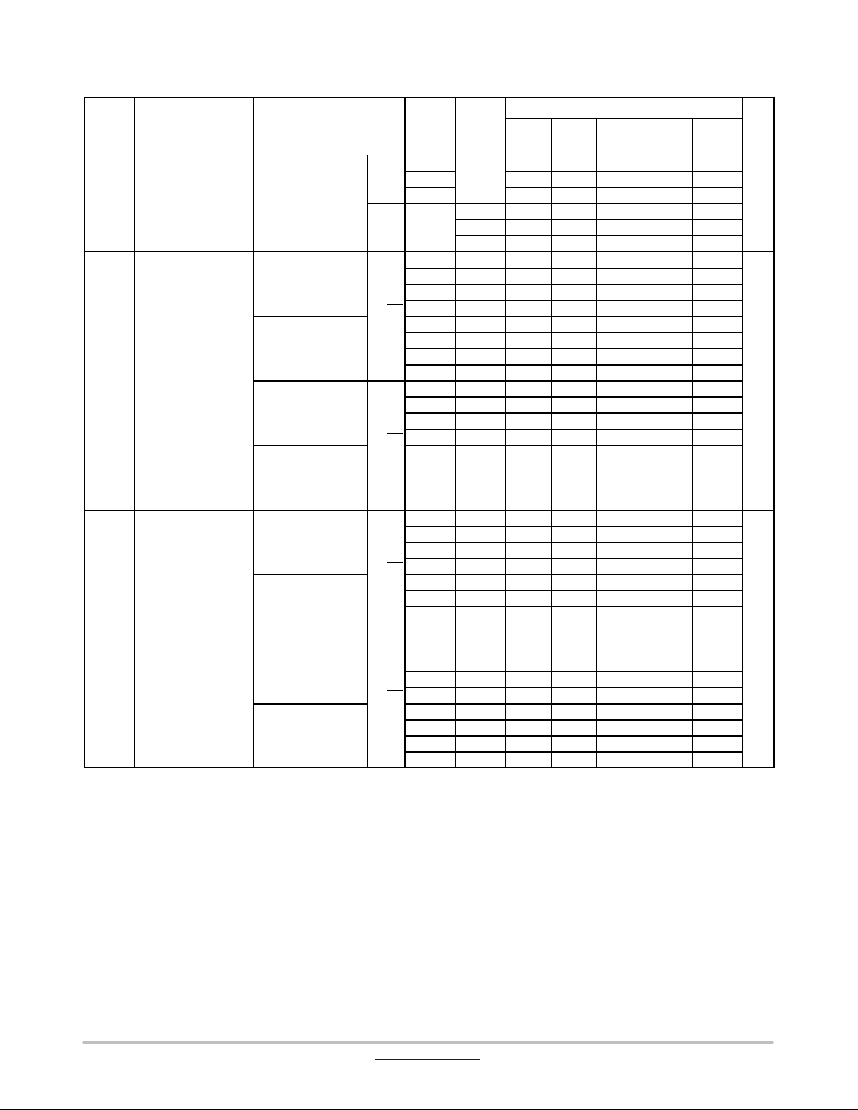
Table 1. MAXIMUM RATINGS
Symbol Parameter Value Condition Unit
V
CCA
V
CCB
V
IN
I
IK
I
OK
I
CCA
I
CCB
I
GND
T
STG
Stresses exceeding those listed in the Maximum Ratings table may damage the device. If any of these limits are exceeded, device functionality
should not be assumed, damage may occur and reliability may be affected.
Table 2. RECOMMENDED OPERATING CONDITIONS
Symbol Parameter Min Max Unit
V
CCA
V
CCB
V
I
T
A
nt/nV Input Transition Rise or Fall Rate
Functional operation above the stresses listed in the Recommended Operating Ranges is not implied. Extended exposure to stresses beyond the
Recommended
A−side DC Supply Voltage −0.5 to +4.6 V
B−side DC Supply Voltage −0.5 to +4.6 V
Input/Output Voltage EN/EN −0.5 to +4.6 V
Power Down Mode (V
CCA
and/or V
= 0 V) −0.5 to +4.6
CCB
Tri−State Mode (EN = L or EN = H) −0.5 to +4.6
Active Mode A−Port −0.5 to V
B−Port −0.5 to V
CCA
CCB
+0.5
+0.5
DC Input Diode Current −50 VIN < GND mA
DC Output Diode Current −50 VO < GND mA
DC Supply Current Through V
DC Supply Current Through V
CCA
CCB
±100 mA
±100 mA
DC Ground Current Through Ground Pin ±100 mA
Storage T
emperature
−65 to +150 °C
A−Port Supply Voltage 0.9 3.6 V
B−Port Supply Voltage 0.9 3.6 V
Input/Output Voltage EN/EN GND 3.6 V
Power Down Mode (V
CCA
and/or V
= 0 V) GND 3.6
CCB
Tri−State Mode (EN = L or EN = H) GND 3.6
Active Mode A−Port GND V
B−Port GND V
CCA
CCB
Operating Temperature Range −40 +125 °C
VI from 30% to 70% of V
CCA/VCCB
0 10 nS
Operating Ranges limits may affect device reliability.
www.onsemi.com
4
Page 5
NLSX5004, NLSXN5004
Table 3. DC ELECTRICAL CHARACTERISTICS
−405C to +855C −405C to +1255C
Typ
(Note 2)
Symbol Parameter Test Conditions (Note 1) Pin/Port V
V
IH
Input HIGH
Voltage
A, EN/EN 0.9−3.6 0.9−3.6 0.65 *
CCA
(V) V
CCB
(V)
Min
V
CCA
B 0.9−3.6 0.9−3.6 0.65 *
V
CCB
V
IL
Input LOW
Voltage
A, EN/EN 0.9−3.6 0.9−3.6 − − 0.35 *
B 0.9−3.6 0.9−3.6 − − 0.35 *
V
OH
Output HIGH
Voltage
IOH = −20 mA A 0.9−3.6 0.9−3.6 0.9 *
V
CCA
B 0.9−3.6 0.9−3.6 0.9 *
V
CCB
V
Output LOW
OL
Voltage
I
Tristate Output
OZ
Leakage
I
Input Pin
I
Leakage
I
Supply Current (EN = V
CC
I
Tristate Output
CCZ
Mode Supply
Current
I
Power Off
OFF
Leakage
IOL = 20 mA A 0.9−3.6 0.9−3.6 − − 0.2 − 0.2 V
B 0.9−3.6 0.9−3.6 − − 0.2 − 0.2 V
(EN = 0V or EN = V
(A = 0 V or V
(B = 0 V or V
VIN = 0 V to V
IO = 0 A, (A = 0 V, B = 0 V)
or (A = V
CCA
CCB
CCA
or EN = 0 V);
CCA
, B = V
CCA
(EN = 0V or EN = V
(A = 0 V, B = 0 V) or
(A = V
CCA
, B = V
A = 0 to 3.6 V,
B = 0 to 3.6 V
); mA
CCA
) A 0.9−3.6 0.9−3.6 − 0.01 ±1.5 − ±4.5
) B 0.9−3.6 0.9−3.6 − 0.01 ±1 − ±3.5
EN/EN 0.9−3.6 0.9−3.6 − 0.01 ±1 − ±3 mA
CCB
CCB
CCA
)
V
V
)
),
V
V
0.9−3.6 0.9−3.6 − 0.4 2.0 − 6.0 mA
CCA
0.9−3.6 0.9−3.6 − 0.3 1.5 − 6.0
CCB
0.9−3.6 0.9−3.6 − 0.2 1.5 − 7.0 mA
CCA
0.9−3.6 0.9−3.6 − 0.2 1.5 − 6.0
CCB
A, B 0 0 − 0.02 1.5 − 5.0 mA
0.9−3.6 0 − 0.01 1.5 − 5.0
0 0.9−3.6 − 0.01 1.5 − 5.0
Product parametric performance is indicated in the Electrical Characteristics for the listed test conditions, unless otherwise noted. Product
performance may not be indicated by the Electrical Characteristics if operated under different conditions.
1. Normal test conditions are VI = 0 V, CLA ≤ 15 pF and CLB ≤ 15 pF, unless otherwise specified.
2. Typical values are for TA = +25°C. All units are production tested at TA = +25°C. Limits over the operating temperature range are guaranteed
by design.
Max Min Max
− − 0.65 *
V
CCA
− − 0.65 *
V
CCB
− 0.35 *
V
CCA
− 0.35 *
V
CCB
− − 0.9 *
V
CCA
− − 0.9 *
V
CCB
− V
− V
V
CCA
V
CCB
− V
− V
Unit
V
V
www.onsemi.com
5
Page 6

NLSX5004, NLSXN5004
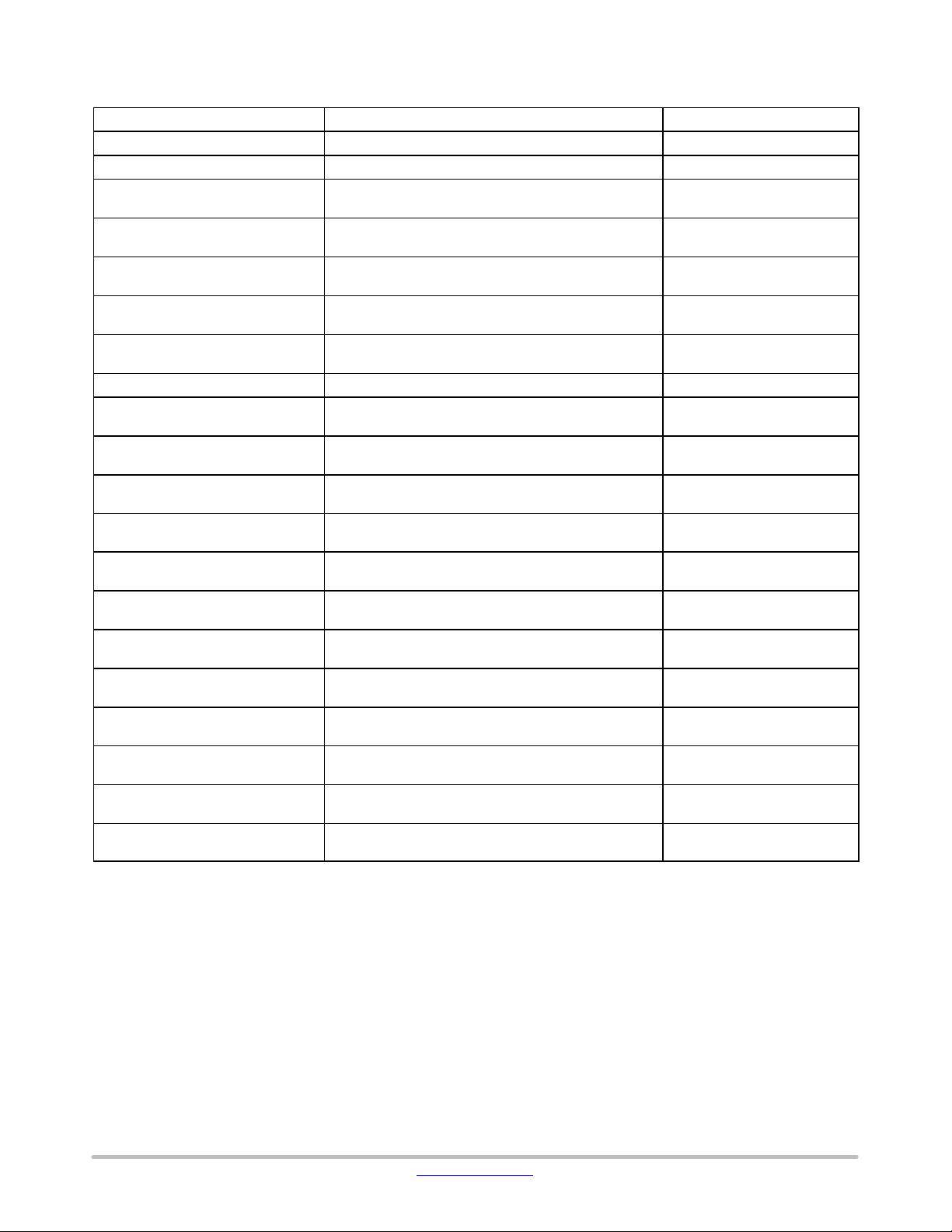
Table 4. TIMING CHARACTERISTICS
−405C to +855C −405C to +1255C
Typ
(Note 4)
Symbol Parameter Test Conditions (Note 3) V
CCA
(V) V
CCB
0.9−3.6 0.9−3.6 − 8.8 30 − 35
1.2 1.8 − 7.3 9 − 9
1.8 1.2 − 9.9 12 − 12
A to B
1.8 2.8 − 4.9 7 − 7
2.8 1.8 − 5.8 7.5 − 7.5
1.8 3.3 − 4.6 6 − 6
3.3 1.8 − 5.7 7 − 7
CL = 15 pF
1.8–3.6 1.8–3.6 − 4.3 9.5 − 10
0.9–3.6 0.9–3.6 − 8.8 30 − 35
1.2 1.8 − 9.9 12 − 12
1.8 1.2 − 7.3 9 − 9
B to A
1.8 2.8 − 5.8 7.5 − 7.5
2.8 1.8 − 4.9 7 − 7
1.8 3.3 − 5.7 7 − 7
3.3 1.8 − 4.6 6 − 6
1.8–3.6 1.8–3.6 − 4.3 9.5 − 10
0.9–3.6 0.9–3.6 − 9.1 32 − 35
1.2 1.8 − 7.8 9.3 − 9.3
1.8 1.2 − 10.8 12.6 − 12.6
A to B
1.8 2.8 − 6.2 7.4 − 7.4
2.8 1.8 − 6.0 7.9 − 7.9
1.8 3.3 − 6.1 7.4 − 7.4
3.3 1.8 − 4.2 6.5 − 6.5
t
Propagation Delay
PD
CL = 30 pF
1.8−3.6 1.8–3.6 − 4.5 10 − 10.5
0.9–3.6 0.9–3.6 − 9.1 32 − 35
1.2 1.8 − 10.8 12.6 − 12.6
1.8 1.2 − 7.8 9.3 − 9.3
B to A
1.8 2.8 − 6.0 7.9 − 8.0
2.8 1.8 − 6.2 7.4 − 7.4
1.8 3.3 − 4.2 6.5 − 6.5
3.3 1.8 − 6.1 7.4 − 7.4
1.8−3.6 1.8–3.6 − 4.5 10 − 10.5
0.9–3.6 0.9–3.6 − 9.4 35 − 37
1.2 1.8 − 8.1 9.5 − 9.5
1.8 1.2 − 11.1 13.6 − 13.6
A to B
1.8 2.8 − 6.5 7.6 − 7.6
2.8 1.8 − 6.2 8.2 − 8.3
1.8 3.3 − 6.3 7.6 − 7.6
3.3 1.8 − 4.3 6.6 − 6.6
CL = 50 pF
1.8–3.6 1.8–3.6 − 4.7 10.3 − 10.8
0.9–3.6 0.9–3.6 − 9.4 35 − 37
1.2 1.8 − 11.1 13.6 − 13.6
1.8 1.2 − 8.1 9.5 − 9.5
B to A
1.8 2.8 − 6.2 8.2 − 8.3
2.8 1.8 − 6.5 7.6 − 7.6
1.8 3.3 − 4.3 6.6 − 6.6
3.3 1.8 − 6.3 7.6 − 7.6
1.8–3.6 1.8–3.6 − 4.7 10.3 − 10.8
3. Typical values are for TA = +25°C. Limits over the operating temperature range are guaranteed by design.
4. Guaranteed by design.
(V)
Min
Max Min Max
Unit
ns
www.onsemi.com
6
Page 7
NLSX5004, NLSXN5004
Table 4. TIMING CHARACTERISTICS (continued)
−405C to +1255C−405C to +855C
Typ
Symbol Unit
CCA
(V)Test Conditions (Note 3)Parameter
V
(V)V
CCB
(Note 4)
Min
0.9–3.6 0.9–3.6 − 9.9 − − −
1.2 1.8 − 8.4 10 − 10
1.8 1.2 − 11.5 14 − 14
A to B
1.8 2.8 − 5.5 8.3 − 8.3
2.8 1.8 − 6.9 8.9 − 9.0
1.8 3.3 − 5.1 6.7 − 6.8
3.3 1.8 − 6.8 8.2 − 8.2
t
Propagation Delay CL = 100 pF
PD
1.8–3.6 1.8–3.6 − 5.0 11 − 11.5
0.9–3.6 0.9–3.6 − 9.9 − − −
1.2 1.8 − 11.5 14 − 14
1.8 1.2 − 8.4 10 − 10
B to A
1.8 2.8 − 6.9 8.9 − 9.0
2.8 1.8 − 5.5 8.3 − 8.3
1.8 3.3 − 6.8 8.2 − 8.2
3.3 1.8 − 5.1 6.7 − 6.8
1.8–3.6 1.8–3.6 − 5.0 11 − 11.5
t
Output Rise Time trial CL = 15 pF
R
0.9–1.2
1.2–1.8 − 2.0 3.0 − 3.0
A
1.8–2.8 − 0.6 2.0 − 2.0
0.9–3.6
2.8–3.6 − 0.5 2.5 − 2.5
0.9–1.2 − 2.5 4.5 − 4.5
B 0.9–3.6
1.2–1.8 − 2.0 3.0 − 3.0
1.8–2.8 − 0.6 2.0 − 2.0
− 2.5 4.5 − 4.5
2.8–3.6 − 0.5 2.5 − 2.5
t
Output Fall Time trial CL = 15 pF
F
0.9–1.2
1.2–1.8 − 1.8 3.0 − 3.0
A
1.8–2.8 − 0.6 2.0 − 2.0
0.9–3.6
2.8–3.6 − 0.5 2.5 − 2.5
0.9–1.2 − 2.5 6.0 − 6.0
B 0.9–3.6
1.2–1.8 − 1.8 3.0 − 3.0
1.8–2.8 − 0.6 2.0 − 2.0
− 2.5 6.0 − 6.0
2.8–3.6 − 0.5 2.5 − 2.5
Channel−to−Channel
t
SK
Skew
MDR Maximum Data Rate
I
I_PEAK
Input Driver Peak
Current
CL = 15 pF
CL = 30 pF
CL = 50 pF
CL = 100 pF
EN = V
EN = 0 V
CCA
or
A = 1 MHz Sq Wave,
Amplitude = V
CCA
B = 1 MHz Sq Wave,
Amplitude = V
CCB
0.9–3.6 0.9–3.6 − − 0.15 − 0.15 ns
0.9–3.6 0.9–3.6 50 − − 50 −
1.8–3.6 1.8–3.6 140 − − 140 −
0.9–3.6 0.9–3.6 40 − − 40 −
1.8–3.6 1.8–3.6 120 − − 120 −
0.9–3.6 0.9−3.6 30 − − 30 −
1.8–3.6 1.8–3.6 100 − − 100 −
0.9–3.6 0.9–3.6 20 − − 20 −
1.8–3.6 1.8–3.6 60 − − 60 −
A 0.9–3.6 0.9–3.6 − − 5.0 − 5.0
B 0.9–3.6 0.9–3.6 − − 5.0 − 5.0
3. Typical values are for TA = +25°C. Limits over the operating temperature range are guaranteed by design.
4. Guaranteed by design.
MaxMinMax
ns
ns
ns
Mbps
mA
www.onsemi.com
7
Page 8
NLSX5004, NLSXN5004
Table 4. TIMING CHARACTERISTICS (continued)
−405C to +1255C−405C to +855C
Typ
Symbol Unit
CCA
(V)Test Conditions (Note 3)Parameter
0.9
1.8 − 20 − − −
A
Z
O
(Note 4)
1−Shot Output
Impedance
3.6 − 10 − − −
B 0.9–3.6
V
(V)V
CCB
− 37 − − −
0.9–3.6
0.9 − 37 − − −
1.8 − 20 − − −
(Note 4)
Min
3.6 − 10 − − −
0.9–3.6 0.9–3.6 − 116.3 200 − 200
1.2–1.8 1.2–1.8 − 64.5 180 − 180
1.8–2.8 1.8–2.8 − 49.6 150 − 150
1.8–3.6 1.8–3.6 − 42.5 100 − 100
EN/EN
to A
0.9–3.6 0.9–3.6 − 113.4 300 − 300
1.2–1.8 1.2–1.8 − 100 250 − 250
1.8–2.8 1.8–2.8 − 94.3 200 − 200
1.8–3.6 1.8–3.6 − 90.9 170 − 170
0.9–3.6 0.9–3.6 − 116.3 200 − 200
1.2–1.8 1.2–1.8 − 64.5 180 − 180
1.8–2.8 1.8–2.8 − 49.6 150 − 150
1.8–3.6 1.8–3.6 − 42.5 100 − 100
EN/EN
to B
0.9–3.6 0.9–3.6 − 113.4 300 − 300
1.2–1.8 1.2–1.8 − 100 250 − 250
1.8–2.8 1.8–2.8 − 94.3 200 − 200
t
Output Enable Time
EN
CL = 15 pF; B = V
CL = 15 pF; B = 0 V
CL = 15 pF; A = V
CL = 15 pF; A = 0 V
CCB
CCA
1.8–3.6 1.8–3.6 − 90.9 170 − 170
0.9–3.6 0.9–3.6 − 255 600 − 600
1.2–1.8 1.2–1.8 − 180 350 − 350
1.8–2.8 1.8–2.8 − 166.7 350 − 350
1.8–3.6 1.8–3.6 − 155.6 300 − 300
EN/EN
to A
0.9–3.6 0.9–3.6 − 156.7 400 − 400
1.2–1.8 1.2–1.8 − 140 300 − 300
1.8–2.8 1.8–2.8 − 130.2 300 − 300
1.8–3.6 1.8–3.6 − 124.6 250 − 250
0.9–3.6 0.9–3.6 − 255 600 − 600
1.2–1.8 1.2–1.8 − 180 350 − 350
1.8–2.8 1.8–2.8 − 166.7 350 − 350
1.8–3.6 1.8–3.6 − 155.6 300 − 300
EN/EN
0.9–3.6 0.9–3.6 − 156.7 400 − 400
to B
1.2–1.8 1.2–1.8 − 140 300 − 300
1.8–2.8 1.8–2.8 − 130.2 300 − 300
t
Output Disable Time
DIS
CL = 15 pF; B = V
CL = 15 pF; B = 0 V
CL = 15 pF; A = V
CL = 15 pF; A = 0 V
CCB
CCA
1.8–3.6 1.8–3.6 − 124.6 250 − 250
3. Typical values are for TA = +25°C. Limits over the operating temperature range are guaranteed by design.
4. Guaranteed by design.
MaxMinMax
W
ns
ns
ns
www.onsemi.com
8
Page 9

NLSX5004, NLSXN5004
NLSX500n
V
/
V
CCA
CCA
EN/EN
EN/EN
V
CCA
V
CCA
GND
A
V
V
CCB
CCB
V
CCB
V
CCA
V
/
CCA
GND
B
C
LB
C
A
LA
NLSX500n
V
V
CCA
CCA
EN/EN
EN/EN
V
V
CCB
CCB
SOURCE
Figure 8. Driving A−Port Test Circuit (tPD) Figure 9. Driving B−Port Test Circuit (tPD)
INPUT
A or B
OUTPUT
B or A
90%
50%
10%
90%
50%
10%
t
PHL
Input
t
r/tf
v3ns
GND
t
F
V
OL
V
CC
t
PLH
t
R
V
OH
V
CCB
B
SOURCE
Figure 10. t
NLSX500n
NLSX500n
EN/EN
EN/EN
SOURCE
A/B
V
/
CCA
V
CCB
B/A
Figure 11. Enable/Disable Test Circuit (t
EN
INPUT
A or B
EN
OUTPUT
B or A
PD
15 pF
(t
PLH/tPHL
50 kΩ
PZH/tPHZ
) Propagation Delay Measurements
NLSX500n
NLSX500n
EN/EN
EN/EN
SOURCE
A/B
B/A
) Figure 12. Enable/Disable Test Circuit (t
V
CCA
V
/2
CCA
GND
t
PZL
50%
V
OL
V
OH
t
PZH
50%
t
PLZ
High
Impedance
10%
90%
t
PHZ
High
Impedance
2* (V
15 pF
CCB/VCCA
50 kΩ
50 kΩ
PZL/tPLZ
)
)
Figure 13. t
EN/tDIS
(t
PZL/tPLZ/tPZH/tPHZ
www.onsemi.com
) Propagation Delay Measurements
9
Page 10

NLSX5004, NLSXN5004
IMPORTANT APPLICATIONS INFORMATION
Level Translator Architecture
The NLSX5004 and the NLSXN5004 auto−sense
translators provide bi−directional logic voltage level
shifting to transfer data in multiple supply voltage systems.
These level translators have two supply voltages, V
V
, which set the logic levels on the input and output
CCB
CCA
and
sides of the translator. When used to transfer data from the
A to the B ports, input signals referenced to the V
CCA
supply are translated to output signals with a logic level
matched to V
. In a similar manner, the B to A
CCB
translation shifts input signals with a logic level compatible
to V
to an output signal matched to V
CCB
CCA
.
The NLSX5004 and the NLSXN5004 translators consist
of bi−directional channels that independently determine
the direction of the data flow without requiring a
directional pin. One−shot circuits are used to detect the
rising or falling input signals. In addition, the one−shots
decrease the rise and fall times of the output signal for
high−to−low and low−to−high transitions.
Input Driver Requirements
The NLSX5004 and NLSXN5004 support high data
rates, but these translators have relatively modest DC
output current drive. The high data rate of the
bi−directional I/O circuit is used to quickly transform from
an input to an output driver and vice versa. Each I/O port
has a modest DC current output so that the internal output
driver can be over−driven when data is sent in the opposite
direction. For proper operation, the input driver to the
auto−sense translator should be capable of driving 5.0 mA
of peak output current. The bi−directional configuration of
the translator results in both input stages being active for a
very short time period. Although the peak current required
from the input signal circuit is relatively large, the average
current is small and consistent with a standard CMOS input
stage.
Enable Input (EN/EN)
The NLSX5004 and NLSXN5004 translators have
enable pins that provide tri−state operation at the I/O ports.
Driving the NLSX5004 Enable pin (EN) to a low logic
level minimizes the power consumption of the device and
drives the A− and B−ports to high impedance states.
Normal translation operation occurs when the EN pin is
equal to a logic high signal.
Driving NLSXN5004 Enable pin (EN) to a high logic
level minimizes the power consumption of the device and
drives the A− and B−ports to high impedance states.
Normal translation operation occurs when the EN pin is
equal to a logic low signal.
Both EN and EN pins are referenced to the V
CCA
supply
and are Over−Voltage Tolerant (OVT).
Uni−Directional versus Bi−Directional Translation
The NLSX5004 and NLSXN5004 translators can
function as non−inverting uni−directional translators. One
advantage of using these translators as uni−directional
devices is that each I/O−port can be configured as either an
input or an output. The configurable input or output feature
is especially useful in applications such as SPI that use
multiple uni−directional I/O lines to send data to and from
a device. The flexible I/O port of the auto sense translator
simplifies the trace connections on the PCB.
Power Supply Guidelines
The values of the V
CCA
and V
supplies can be set to
CCB
anywhere between 0.9 and 3.6 V. Design flexibility is
maximized because V
to or less than the V
may be either greater than, equal
CCA
supply.
CCB
The sequencing of the power supplies will not damage
the device during power−up operation. In addition, the A−
and B−ports are in high impedance states if either supply
voltage is equal to 0 V. For optimal performance, 0.01 to
0.1 µF decoupling capacitors should be used on the V
and V
power supply pins. Ceramic capacitors are a
CCB
CCA
good design choice to filter and bypass any noise signals on
the voltage lines to the ground plane of the PCB. The noise
immunity will be maximized by placing the capacitors as
close as possible to the supply and ground pins, along with
minimizing the PCB connection traces.
www.onsemi.com
10
Page 11
NLSX5004, NLSXN5004
DEVICE ORDERING INFORMATION
Device Order Number Package Type Tape & Reel Size
NLSX5004MUTAG UQFN−12 3000 Units/Reel
NLVSX5004MUTAG* UQFN−12 3000 Units/Reel
NLSX5004DR2G
(In Development)
NLVSX5004DR2G*
(In Development)
NLSX5004DTR2G
(In Development)
NLVSX5004DTR2G*
(In Development)
NLSX5004MN1TXG
(In Development)
NLVSX5004MN1TXG* QFN14, 3.5 x 3.5 x 0.5P 3000 Units/Reel
NLSX5004MN1TWG
(In Development)
NLVSX5004MN1TWG*
(In Development)
NLSXN5004MU2TAG
(In Development)
NLVSXN5004MU2TAG*
(In Development)
NLSXN5004DR2G
(In Development)
NLVSXN5004DR2G*
(In Development)
NLSXN5004DTR2G
(In Development)
NLVSXN5004DTR2G*
(In Development)
NLSXN5004MN1TXG
(In Development)
NLVSXN5004MN1TXG*
(In Development)
NLSXN5004MN1TWG
(In Development)
NLVSXN5004MN1TWG*
(In Development)
†For information on tape and reel specifications, including part orientation and tape sizes, please refer to our Tape and Reel Packaging
Specifications Brochure, BRD8011/D.
*NLV Prefix for Automotive and Other Applications Requiring Unique Site and Control Change Requirements; AEC−Q100 Qualified and PPAP
Capable
SOIC14 2500 Units/Reel
SOIC14 2500 Units/Reel
TSSOP14 2500 Units/Reel
TSSOP14 2500 Units/Reel
QFN14, 3.5 x 3.5 x 0.5P 3000 Units/Reel
QFN14, 2.5 x 3.0 x 0.5P 3000 Units/Reel
QFN14, 2.5 x 3.0 x 0.5P 3000 Units/Reel
UQFN−12 3000 Units/Reel
UQFN−12 3000 Units/Reel
SOIC14 2500 Units/Reel
SOIC14 2500 Units/Reel
TSSOP14 2500 Units/Reel
TSSOP14 2500 Units/Reel
QFN14, 3.5 x 3.5 x 0.5P 3000 Units/Reel
QFN14, 3.5 x 3.5 x 0.5P 3000 Units/Reel
QFN14, 2.5 x 3.0 x 0.5P 3000 Units/Reel
QFN14, 2.5 x 3.0 x 0.5P 3000 Units/Reel
†
www.onsemi.com
11
Page 12

PIN 1 REFERENCE
0.10 C
2X
2X
0.10 C
0.05 C
12X
0.05 C
8X
DETAIL A
TOP VIEW
A3
SIDE VIEW
K
1
L12X
BOTTOM VIEW
D AEB
DETAIL B
A
A1
C
75
e
11
L2
NLSX5004, NLSXN5004
PACKAGE DIMENSIONS
UQFN12 1.7x2.0, 0.4P
CASE 523AE
ISSUE A
L1
DETAIL A
NOTE 5
DETAIL B
OPTIONAL
CONSTRUCTION
SEATING
PLANE
12X
b
0.10
0.05
M
M
C
BAC
NOTE 3
2.30
NOTES:
1. DIMENSIONING AND TOLERANCING PER ASME
Y14.5M, 1994.
2. CONTROLLING DIMENSION: MILLIMETERS
3. DIMENSION b APPLIES TO PLATED TERMINAL
AND IS MEASURED BETWEEN 0.15 AND 0.30 MM
FROM TERMINAL TIP.
4. MOLD FLASH ALLOWED ON TERMINALS
ALONG EDGE OF PACKAGE. FLASH 0.03
MAX ON BOTTOM SURFACE OF
TERMINALS.
5. DETAIL A SHOWS OPTIONAL
CONSTRUCTION FOR TERMINALS.
MILLIMETERS
DIM MIN MAX
A
0.45 0.55
A1
0.00 0.05
0.127 REF
A3
0.15 0.25
b
D
1.70 BSC
E
2.00 BSC
0.40 BSC
e
K
0.20 ----
0.45 0.55
L
0.00 0.03L1
0.15 REF
L2
MOUNTING FOOTPRINT
SOLDERMASK DEFINED
2.00
1
0.32
11X
0.22
0.40
PITCH
www.onsemi.com
12
12X
0.69
DIMENSIONS: MILLIMETERS
Page 13

14
H
M
0.25 B
0.10
NLSX5004, NLSXN5004
PACKAGE DIMENSIONS
SOIC−14 NB
CASE 751A−03
D
A
ISSUE L
B
8
A3
E
L
71
M
b13X
S
M
0.25 B
A
C
S
A
e
A1
C
SEATING
PLANE
DETAIL A
h
X 45
_
M
DETAIL A
NOTES:
1. DIMENSIONING AND TOLERANCING PER
ASME Y14.5M, 1994.
2. CONTROLLING DIMENSION: MILLIMETERS.
3. DIMENSION b DOES NOT INCLUDE DAMBAR
PROTRUSION. ALLOWABLE PROTRUSION
SHALL BE 0.13 TOTAL IN EXCESS OF AT
MAXIMUM MATERIAL CONDITION.
4. DIMENSIONS D AND E DO NOT INCLUDE
MOLD PROTRUSIONS.
5. MAXIMUM MOLD PROTRUSION 0.15 PER
SIDE.
DIM MIN MAX MIN MAX
A 1.35 1.75 0.054 0.068
A1 0.10 0.25 0.004 0.010
A3 0.19 0.25 0.008 0.010
b 0.35 0.49 0.014 0.019
D 8.55 8.75 0.337 0.344
E 3.80 4.00 0.150 0.157
e 1.27 BSC 0.050 BSC
H 5.80 6.20 0.228 0.244
h 0.25 0.50 0.010 0.019
L 0.40 1.25 0.016 0.049
M 0 7 0 7
____
INCHESMILLIMETERS
SOLDERING FOOTPRINT*
6.50
1
14X
0.58
DIMENSIONS: MILLIMETERS
*For additional information on our Pb−Free strategy and soldering
details, please download the ON Semiconductor Soldering and
Mounting Techniques Reference Manual, SOLDERRM/D.
14X
1.18
1.27
PITCH
www.onsemi.com
13
Page 14

0.10 (0.004)
−T−
SEATING
PLANE
NLSX5004, NLSXN5004
PACKAGE DIMENSIONS
TSSOP−14 WB
CASE 948G
U
ISSUE C
S
N
S
0.25 (0.010)
U0.15 (0.006) T
S
2X L/2
14X REFK
0.10 (0.004) V
14
M
T
8
M
L
PIN 1
IDENT.
1
S
U0.15 (0.006) T
A
−V−
B
N
−U−
F
7
DETAIL E
K
K1
J J1
SECTION N−N
C
D
G
H
DETAIL E
NOTES:
1. DIMENSIONING AND TOLERANCING PER
ANSI Y14.5M, 1982.
2. CONTROLLING DIMENSION: MILLIMETER.
3. DIMENSION A DOES NOT INCLUDE MOLD
FLASH, PROTRUSIONS OR GATE BURRS.
MOLD FLASH OR GATE BURRS SHALL NOT
EXCEED 0.15 (0.006) PER SIDE.
4. DIMENSION B DOES NOT INCLUDE
INTERLEAD FLASH OR PROTRUSION.
INTERLEAD FLASH OR PROTRUSION SHALL
NOT EXCEED 0.25 (0.010) PER SIDE.
5. DIMENSION K DOES NOT INCLUDE DAMBAR
PROTRUSION. ALLOWABLE DAMBAR
PROTRUSION SHALL BE 0.08 (0.003) TOTAL
IN EXCESS OF THE K DIMENSION AT
MAXIMUM MATERIAL CONDITION.
6. TERMINAL NUMBERS ARE SHOWN FOR
REFERENCE ONLY.
7. DIMENSION A AND B ARE TO BE
DETERMINED AT DATUM PLANE −W−.
INCHESMILLIMETERS
−W−
DIM MIN MAX MIN MAX
A 4.90 5.10 0.193 0.200
B 4.30 4.50 0.169 0.177
C −−− 1.20 −−− 0.047
D 0.05 0.15 0.002 0.006
F 0.50 0.75 0.020 0.030
G 0.65 BSC 0.026 BSC
H 0.50 0.60 0.020 0.024
J 0.09 0.20 0.004 0.008
J1 0.09 0.16 0.004 0.006
K 0.19 0.30 0.007 0.012
K1 0.19 0.25 0.007 0.010
L 6.40 BSC 0.252 BSC
M 0 8 0 8
____
14X
0.36
SOLDERING FOOTPRINT
7.06
1
14X
1.26
0.65
PITCH
DIMENSIONS: MILLIMETERS
www.onsemi.com
14
Page 15
REFERENCE
2X
2X
NOTE 4
PIN ONE
DETAIL A
C0.10
C0.05
C0.05
C0.10
SIDE VIEW
6
D
TOP VIEW
DETAIL B
D2
7
8
NLSX5004, NLSXN5004
PACKAGE DIMENSIONS
QFN14, 2.5x3.0, 0.5P
CASE 485DE
ISSUE O
NOTES:
A
L
L
B
L1
DETAIL A
ALTERNATE TERMINAL
E
A
(A3)
CONSTRUCTIONS
MOLD CMPDEXPOSED Cu
DETAIL B
ALTERNATE
CONSTRUCTIONS
A1
SEATING
C
PLANE
14X
L
9
1. DIMENSIONING AND TOLERANCING PER
ASME Y14.5M, 1994.
2. CONTROLLING DIMENSION: MILLIMETERS.
3. DIMENSIONS b APPLIES TO PLATED
TERMINAL AND IS MEASURED BETWEEN
0.15 AND 0.25MM FROM THE TERMINAL TIP.
4. COPLANARITY APPLIES TO THE EXPOSED
PAD AS WELL AS THE TERMINALS.
MILLIMETERS
DIM MIN MAX
A
0.80 1.00
A1 0.00 0.05
A3
0.20 REF
b 0.20 0.30
D 2.50 BSC
D2 0.90 1.10
E 3.00 BSC
E2
1.40 1.60
e 0.50 BSC
L 0.30 0.50
L1 --- 0.05
RECOMMENDED
SOLDERING FOOTPRINT*
2.80
1.18
1
14X
0.63
NOTE 3
M
0.10 C
M
0.05 C
14X
1.68
E2
14X
2
b
A
B
1
e
13
14
e/2
BOTTOM VIEW
*For additional information on our Pb−Free strategy and soldering
0.32
0.50
PITCH
DIMENSIONS: MILLIMETERS
3.33
PACKAGE
OUTLINE
details, please download the ON Semiconductor Soldering and
Mounting Techniques Reference Manual, SOLDERRM/D.
www.onsemi.com
15
Page 16

ÎÎÎ
ÎÎÎ
2X
2X
NOTE 4
PIN 1
LOCATION
0.15 C
0.15 C
0.10 C
0.08 C
DETAIL B
DETAIL A
14X
L
D
TOP VIEW
SIDE VIEW
D2
7
(A3)
NLSX5004, NLSXN5004
PACKAGE DIMENSIONS
QFN14 3.5x3.5, 0.5P
CASE 485AL
ISSUE O
A
B
EDGE OF PACKAGE
L
L1
DETAIL A
A
C
OPTIONAL PIN
CONSTRUCTION
EXPOSED Cu
SEATING
PLANE
DETAIL B
OPTIONAL PIN
CONSTRUCTION
E
A1
14X
K
9
DETAIL A
OPTIONAL PIN
CONSTRUCTION
MOLD CMPD
SOLDERING FOOTPRINT*
NOTES:
1. DIMENSIONING AND TOLERANCING PER
L
ASME Y14.5M, 1994.
2. CONTROLLING DIMENSION: MILLIMETERS.
3. DIMENSION b APPLIES TO PLATED
TERMINAL AND IS MEASURED BETWEEN
0.15 AND 0.30 MM FROM TERMINAL TIP.
4. COPLANARITY APPLIES TO THE EXPOSED
PAD AS WELL AS THE TERMINALS.
MILLIMETERS
DIM MIN MAX
A 0.80 1.00
A1 0.00 0.05
A3 0.20 REF
b 0.18 0.30
D 3.50 BSC
D2 1.90 2.15
E 3.50 BSC
E2 1.90 2.15
e 0.50 BSC
e2 1.50 BSC
K 0.20 −−−
L 0.30 0.50
L1 0.00 0.03
2X
3.80
14X
0.63
14X
0.36
2.12
E2
e
2
1
e2
BOTTOM VIEW
14
14X
b
0.10 C
0.05 C
A B
NOTE 3
2X
0.50
PITCH
1.50 PITCH
DIMENSIONS: MILLIMETERS
*For additional information on our Pb−Free strategy and soldering
details, please download the ON Semiconductor Soldering and
Mounting Techniques Reference Manual, SOLDERRM/D.
ON Semiconductor and are trademarks of Semiconductor Components Industries, LLC dba ON Semiconductor or its subsidiaries in the United States and/or other countries.
ON Semiconductor owns the rights to a number of patents, trademarks, copyrights, trade secrets, and other intellectual property. A listing of ON Semiconductor’s product/patent
coverage may be accessed at www.onsemi.com/site/pdf/Patent− Marking.pdf. ON Semiconductor reserves the right to make changes without further notice to any products herein.
ON Semiconductor makes no warranty, representation or guarantee regarding the suitability of its products for any particular purpose, nor does ON Semiconductor assume any liability
arising out of the application or use of any product or circuit, and specifically disclaims any and all liability, including without limitation special, consequential or incidental damages.
Buyer is responsible for its products and applications using ON Semiconductor products, including compliance with all laws, regulations and safety requirements or standards,
regardless of any support or applications information provided by ON Semiconductor. “Typical” parameters which may be provided in ON Semiconductor data sheets and/or
specifications
application
designed, intended, or authorized for use as a critical component in life support systems or any FDA Class 3 medical devices or medical devices with a same or similar classification
in a foreign jurisdiction or any devices intended for implantation in the human body. Should Buyer purchase or use ON Semiconductor products for any such unintended or
unauthorized application, Buyer shall indemnify and hold ON Semiconductor and its officers, employees, subsidiaries, affiliates, and distributors harmless against all claims, costs,
damages, and expenses, and reasonable attorney fees arising out of, directly or indirectly, any claim of personal injury or death associated with such unintended or unauthorized
use, even if such claim alleges that ON Semiconductor was negligent regarding the design or manufacture of the part. ON Semiconductor is an Equal Opportunity/Affirmative Action
Employer. This literature is subject to all applicable copyright laws and is not for resale in any manner.
can and do vary in different applications and actual performance may vary over time. All operating parameters, including “Typicals” must be validated for each customer
by customer’s technical experts. ON Semiconductor does not convey any license under its patent rights nor the rights of others. ON Semiconductor products are not
PUBLICATION ORDERING INFORMATION
LITERATURE FULFILLMENT:
Email Requests to: orderlit@onsemi.com
ON Semiconductor Website: www
.onsemi.com
◊
TECHNICAL SUPPORT
North American Technical Support:
Voice Mail: 1 800−282−9855 Toll Free USA/Canada
Phone: 011 421 33 790 2910
www.onsemi.com
Europe, Middle East and Africa Technical Support:
Phone: 00421 33 790 2910
For additional information, please contact your local Sales Representative
16
 Loading...