

Page 1
1 W SPDT Switch
NL5S4157A
The NL5S4157A is a low RON SPDT analog switch. The device is
designed for low operating voltage, high current switching of speaker
output for mobile applications. It can switch a balanced stereo output.
It can handle a balanced microphone/speaker/ringtone generator in
monophone mode.
Features
• Wide V
• OVT up to +5.5 V for Control pin
• R
ON
• Rail−to−Rail Input/Output
• This Device is Pb−Free, Halogen Free/BFR Free and is RoHS
Compliant
Typical Applications
• Cell Phone Speaker/Microphone Switching
• Ringtone−Chip/Amplifier Switching
• Stereo Balanced (Push−Pull) Switching
• RF PA Routing
• General Switching
Operating Range: 1.65 V to 5.5 V
CC
: Typically < 1 W at VCC = 4.5 V
www.onsemi.com
1
SC−88/SC70−6/SOT−363
CASE 419B−02
MARKING DIAGRAM
6
ATM G
G
1
AT = Specific Device Code
M = Date Code*
G = Pb−Free Package
(Note: Microdot may be in either location)
*Date Code orientation and/or position may
vary depending upon manufacturing location.
© Semiconductor Components Industries, LLC, 2020
January, 2021 − Rev. 1
ORDERING INFORMATION
See detailed ordering and shipping information on page 6 of
this data sheet.
1 Publication Order Number:
NL5S4157A/D
Page 2
NL5S4157A
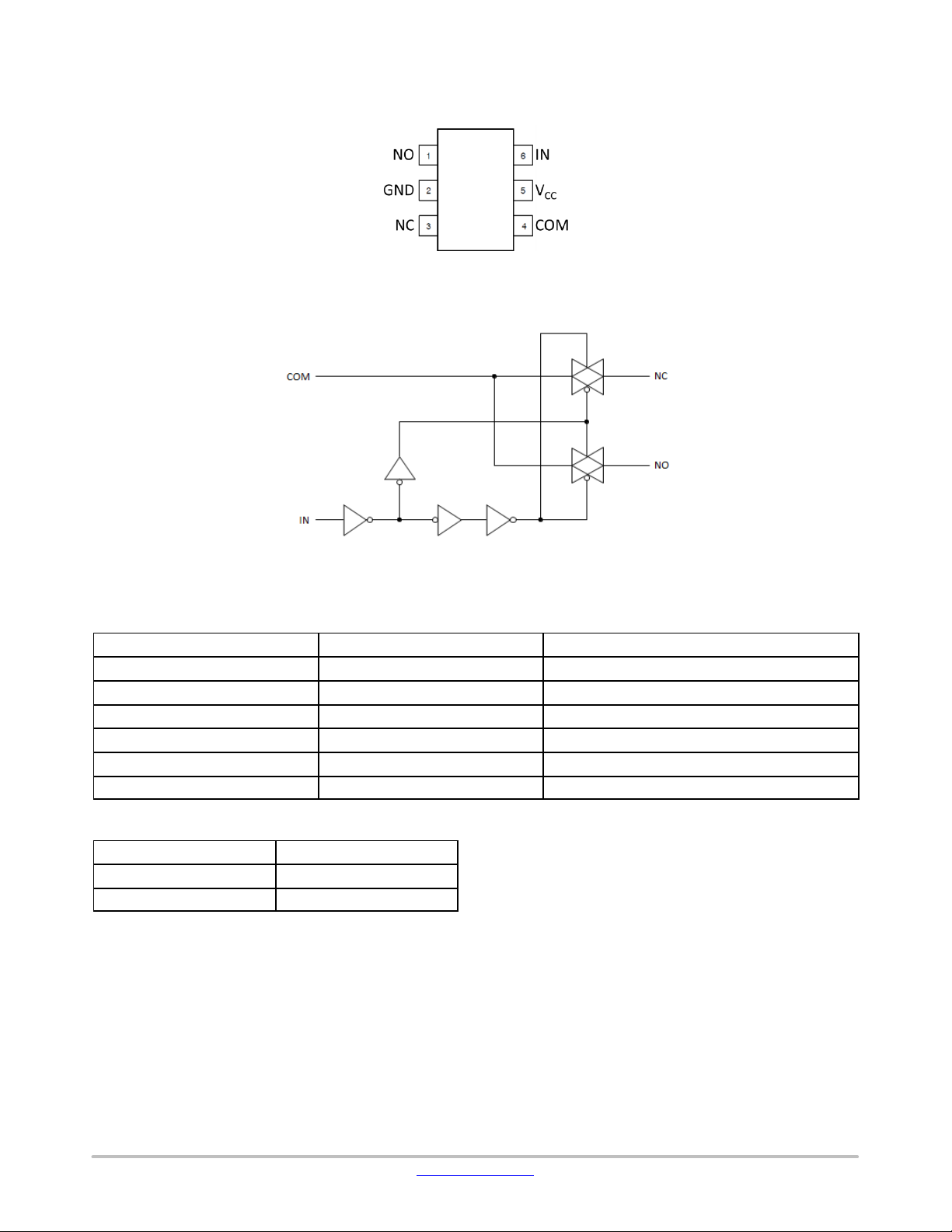
PIN ASSIGNMENTS
Figure 1. NL5S4157A (Top View)
PIN DESCRIPTION
Pin Name Description
1 NO Normally−Open Port
2 GND Supply Ground
3 NC Normally−Closed Port
4 COM Common Port
5 V
6 IN Switch Select Input
FUNCTION TABLE
IN Switch
L NC to COM
H NO to COM
Figure 2. Analog Symbol
CC
Supply
www.onsemi.com
2
Page 3

NL5S4157A
MAXIMUM RATINGS
Symbol Rating Value Unit
V
CC
V
IS
V
IN
I
OK
I
IK
I
I/O
I
I/O−pk
T
s
ESD Human Body Model (HBM) 2 kV
Stresses exceeding those listed in the Maximum Ratings table may damage the device. If any of these limits are exceeded, device functionality
should not be assumed, damage may occur and reliability may be affected.
RECOMMENDED OPERATING CONDITIONS
Symbol Parameter Min Max Unit
V
CC
V
V
T
tr, t
Functional operation above the stresses listed in the Recommended Operating Ranges is not implied. Extended exposure to stresses beyond
the Recommended Operating Ranges limits may affect device reliability.
Positive DC Supply Voltage −0.5 to +6.0 V
Switch Input / Output Voltage −0.5 to VCC+0.5 V
Digital Select Input Voltage −0.5 to +6.0 V
I/O Port Diode Current ±100 mA
Select Input Diode Current −100 mA
Continuous DC Current Through Analog Switch ±100 mA
Peak Current Through Analog Switch, 10% Duty Cycle ±300 mA
Storage Temperature −65 to +150 °C
Positive DC Supply Voltage 1.65 5.5 V
IS
IN
A
f
Switch Input / Output Voltage GND V
Digital Select Input Voltage GND 5.5 V
Operating Temperature Range −40 +125 °C
Input Transition Rise or Fall Time
(Select Input IN)
V
v 3.0 V 0 20 ns/V
CC
V
> 3.0 V 0 10
CC
CC
V
www.onsemi.com
3
Page 4
NL5S4157A
ELECTRICAL CHARACTERISTICS
Guaranteed Limit
255C −405C to 855C −405C to 1255C
Symbol Parameter Condition VCC (V) Min Typ Max Min Max Min Max Unit
V
IH
V
IL
I
IN
I
OFF
I
S(ON)
I
S(OFF)
I
CC
Input High
Voltage
Input Low
Voltage
Input
Leakage
Current
Input
Leakage
Current
ON−State
Switch
Leakage
Current
OFF−State
Switch
Leakage
Current
Quiescent
Supply
Current
V
= 0 V to
IN
5.5 V
V
= 0 to
IN
5.5 V
V
= GND
IS
to V
,
CC
VOS = Open
V
= V
IS
CC
and
VOS = GND,
or
= GND
IS
and
VOS = V
CC
V
= VCC
IN
or GND,
I
= 0 mA
OS
2.7 1.1 1.1 1.1 V
5.0 1.42 1.42 1.42
2.7 0.4 0.4 0.4 V
5.0 0.7 0.7 0.7
1.65 − 5.5 ±0.1 ±1 ±1
0 0.05 1 1
5.5 ±10 ±200 ±600 nA
5.5 ±10 ±200 ±600 nA
5.5 0.5 5 5
mA
mA
mA
www.onsemi.com
4
Page 5

NL5S4157A
ANALOG SWITCH CHARACTERISTICS
Guaranteed Limit
25ºC −40ºC to 125ºC
Symbol Parameter Condition VCC (V)
R
ON
(Note 1)
nR
ON
(Notes 1, 2, 3)
R
FLAT
(Notes 1, 2, 4)
Q
(Note 5)
V
ISO
(Note 6)
V
CT
Switch ON Resistance VIS = 0 to
VCC,
I
= 100 mA
O
ON Resistance Match VIS = 1.5 V,
I
= 100 mA
A
Between Channels VIS = 2.5 V,
I
= 100 mA
A
ON Resistance Flatness VIS = 0 to VCC,
I
= 100 mA
O
Charge Injection
CL = 1 nF,
V
= 0 V,
GEN
R
=0 Ω 4.5 55
GEN
Off−Isolation RL = 50 Ω,
f = 1 MHz
Crosstalk RL = 50 Ω,
f = 1 MHz
2.7 0.9 1.2 1.4
4.5 0.6 0.8 1.0
2.7 0.05 0.15 0.15
4.5 0.04 0.12 0.15
2.7 0.3 0.4 0.4
4.5 0.2 0.4 0.4
2.7 38
2.7 – 5.5 −66 dB
2.7 – 5.5 −66 dB
BW −3 dB Bandwidth RL = 50 Ω 2.7 – 5.5 57 MHz
THD
(Note 5)
Total Harmonic Distortion RL = 600 Ω,
V
= 0.5 V
IS
P−P
2.7 – 5.5 0.004 %
,
f = 20 Hz to 20
kHz
C
I
C
OFF
C
ON
Select Input Capacitance f = 1 MHz 0 3.0 pF
NC/NO Port Off Capacitance f = 1 MHz 4.5 23 pF
COM Port ON Capacitance f = 1 MHz 4.5 93 pF
1. Measured by the voltage drop between NC/NO and COM pins at the indicated current through the switch. On Resistance is determined by
the lower of the voltages on the two (NO, NC, COM).
2. Parameter is characterized but not tested in production.
= R
max − R
3. DR
4. Flatness is defined as the difference between the maximum and minimum value of On Resistance over the specified range of conditions.
ON
ON
min measured at identical VCC, temperature and voltage levels.
ON
5. Guaranteed by Design.
6. V
= 20 log10 [V
ISO
COM/VNO,NC
].
Min Typ Max Min Max Unit
Ω
Ω
Ω
pC
www.onsemi.com
5
Page 6

NL5S4157A
SWITCHING CHARACTERISTICS
Guaranteed Limit
255C −405C to 1255C
Symbol Parameter Condition VCC (V) Min Typ Max Min Max Unit
t
PD
(Note 7)
t
ON
t
OFF
T
BBM
(Note 5)
7. This parameter is guaranteed by design but not tested. The bus switch contributes no propagation delay other than the RC delay of the On
Resistance of the switch and the 50 pF load capacitance, when driven by an ideal voltage source (zero output impedance).
Propagation Delay VIN = VIH or V
Turn−on Time,
(COM to NO or NC)
RL = 50 W,
C
= 35 pF,
L
VIS = 1.5 V 2.7 30 35
VIS = 3.0 V 4.5 20 25
RL = 50 W,
C
= 100 pF,
L
VIS = 1.5 V 3.3 100 100
Turn−off Time,
(COM to NO or NC)
RL = 50 W,
C
= 35 pF,
L
VIS = 1.5 V 2.7 20 25
VIS = 3.0 V 4.5 15 20
RL = 50 W,
C
= 100 pF,
L
VIS = 1.5 V 3.3 100 100
Break Before Make Time
RL = 50 W,
C
= 35 pF
L
2.7 2.0 2.0 ns
IL
4.5 0.3 0.3
2.7 0.5 0.5 ns
4.5 0.5 0.5
ns
ns
ORDERING INFORMATION
Pin 1 Orientation
Device Package Marking
(See below)
Shipping
NL5S4157ADFT2G SC*88/SC70*6/SOT*363 AT Q4 3000 / Tape & Reel
†For information on tape and reel specifications, including part orientation and tape sizes, please refer to our Tape and Reel Packaging
Specifications Brochure, BRD8011/D.
†
PIN 1 ORIENTATION IN TAPE AND REEL
Pin 1 Orientation in Tape and Reel
Figure 3.
www.onsemi.com
6
Page 7

Test Setups
NL5S4157A
Figure 4. t
(Time Break−Before−Make)
BBM
Figure 5. tON/t
OFF
Test Set-Up
Figure 6. tON/t
OFF
www.onsemi.com
7
Page 8

V
NL5S4157A
OUT
V
IN
Off−Isolation Crosstalk
V
OUT
V
IN
Channel switch control/s test socket is normalized. Off isolation is measured across an off channel. Crosstalk is measured from an off channel to an on channel. On loss is the bandwidth of an On switch. V
, VCT, Bandwidth and V
ISO
ONL
are independent of the input signal direction.
or VCT = Off Channel Isolation or crosstalk = 20 Log for V
V
ISO
V
= On Channel Loss = 20 Log for V
ONL
OUT
Bandwidth (BW) = the frequency 3 dB below V
/ V
at 100 kHz to 50 MHz
IN
ONL
OUT
/ V
IN
Figure 7. Off Channel Isolation/On Channel Loss (BW)/Crosstalk
(On Channel to Off Channel)/V
ONL
Figure 8. Charge Injection: (Q)
www.onsemi.com
8
Page 9

NL5S4157A
TYPICAL CHARACTERISTICS
0
−10
−20
−30
−40
−50
−60
−70
, NO/NC TO COM (dB)
ISO
−80
V
−90
−100
0.005
0.004
0.003
THD (%)
0.002
0.001
0
−1
−2
−3
BW (dB)
−4
−5
(W)
R
ON
−6
1.1
1.0
0.9
0.8
0.7
0.6
0.5
Figure 10. Bandwidth vs. Frequency
125°C
85°C
25°C
−40°C
1001010.10.01
FREQUENCY (MHz) FREQUENCY (MHz)
Figure 9. V
vs. Frequency
ISO
@ V
= 4.5 V
CC
1001010.10.01
(W)
R
0
FREQUENCY (Hz) VIS (V)
Figure 11. Total Harmonic Distortion Figure 12. ON Resistance vs. Switch Voltage
0.9
0.8
ON
0.7
0.6
0.5
0.4
0.3
0.2
125°C
85°C
25°C
−40°C
2.5 4.5 5.54.53.52.51.50.5
VIS (V) VIS (V)
Figure 13. ON Resistance vs. Switch Voltage
@ V
= 4.5 V
CC
(W)
R
ON
0.4
0.9
0.8
0.7
0.6
0.5
0.4
2.7 V
3.0 V
@ V
3.6 V
= 2.7 V
CC
4.5 V
5.5 V
100K10K1K10010
4.03.53.02.01.51.00.50
3.02.52.01.51.00.50
5.04.03.02.01.00
Figure 14. ON Resistance vs. Switch Voltage
www.onsemi.com
9
Page 10

MECHANICAL CASE OUTLINE
PACKAGE DIMENSIONS
SC−88/SC70−6/SOT−363
1
SCALE 2:1
D
A
654
E
123
2X
bbb H
D
e
B
TOP VIEW
6X
ccc
C
SIDE VIEW END VIEW
RECOMMENDED
SOLDERING FOOTPRINT*
6X
0.30
0.65
PITCH
*For additional information on our Pb−Free strategy and soldering
details, please download the ON Semiconductor Soldering and
Mounting Techniques Reference Manual, SOLDERRM/D.
2X
aaa H D
D
E1
L2
aaa C
2X 3 TIPS
b
6X
M
A2
A
A1
C
6X
0.66
SEATING
PLANE
2.50
DIMENSIONS: MILLIMETERS
Cddd
A-B D
DETAIL A
CASE 419B−02
ISSUE Y
H
L
DETAIL A
GAGE
PLANE
DATE 11 DEC 2012
NOTES:
1. DIMENSIONING AND TOLERANCING PER ASME Y14.5M, 1994.
2. CONTROLLING DIMENSION: MILLIMETERS.
3. DIMENSIONS D AND E1 DO NOT INCLUDE MOLD FLASH,
PROTRUSIONS, OR GATE BURRS. MOLD FLASH, PROTRUSIONS, OR GATE BURRS SHALL NOT EXCEED 0.20 PER END.
4. DIMENSIONS D AND E1 AT THE OUTERMOST EXTREMES OF
THE PLASTIC BODY AND DATUM H.
5. DATUMS A AND B ARE DETERMINED AT DATUM H.
6. DIMENSIONS b AND c APPLY TO THE FLAT SECTION OF THE
LEAD BETWEEN 0.08 AND 0.15 FROM THE TIP.
7. DIMENSION b DOES NOT INCLUDE DAMBAR PROTRUSION.
ALLOWABLE DAMBAR PROTRUSION SHALL BE 0.08 TOTAL IN
EXCESS OF DIMENSION b AT MAXIMUM MATERIAL CONDITION. THE DAMBAR CANNOT BE LOCATED ON THE LOWER
RADIUS OF THE FOOT.
MILLIMETERS
DIM MIN NOM MAX
A −−− −−− 1.10
A1 0.00 −−− 0.10
A2 0.70 0.90 1.00 0.027 0.035 0.039
b 0.15 0.20 0.25
C 0.08 0.15 0.22
D 1.80 2.00 2.20
E
2.00 2.10 2.20
E1 1.15 1.25 1.35
e 0.65 BSC
L 0.26 0.36 0.46
L2 0.15 BSC 0.006 BSC
aaa 0.15 0.006
bbb 0.30 0.012
ccc 0.10 0.004
ddd
c
0.10 0.004
INCHES
MIN NOM MAX
−−− −−− 0.043
0.000 −−− 0.004
0.006 0.008 0.010
0.003 0.006 0.009
0.070 0.078 0.086
0.078 0.082 0.086
0.045 0.049 0.053
0.026 BSC
0.010 0.014 0.018
GENERIC
MARKING DIAGRAM*
6
XXXMG
G
1
XXX = Specific Device Code
M = Date Code*
G = Pb−Free Package
(Note: Microdot may be in either location)
*Date Code orientation and/or position may
vary depending upon manufacturing location.
*This information is generic. Please refer to
device data sheet for actual part marking.
Pb−Free indicator, “G” or microdot “G”, may
or may not be present. Some products may
not follow the Generic Marking.
STYLES ON PAGE 2
DOCUMENT NUMBER:
DESCRIPTION:
ON Semiconductor and are trademarks of Semiconductor Components Industries, LLC dba ON Semiconductor or its subsidiaries in the United States and/or other countries.
ON Semiconductor reserves the right to make changes without further notice to any products herein. ON Semiconductor makes no warranty, representation or guarantee regarding
the suitability of its products for any particular purpose, nor does ON Semiconductor assume any liability arising out of the application or use of any product or circuit, and specifically
disclaims any and all liability, including without limitation special, consequential or incidental damages. ON Semiconductor does not convey any license under its patent rights nor the
rights of others.
© Semiconductor Components Industries, LLC, 2019
98ASB42985B
SC−88/SC70−6/SOT−363
Electronic versions are uncontrolled except when accessed directly from the Document Repository.
Printed versions are uncontrolled except when stamped “CONTROLLED COPY” in red.
PAGE 1 OF 2
www.onsemi.com
Page 11

SC−88/SC70−6/SOT−363
CASE 419B−02
ISSUE Y
DATE 11 DEC 2012
STYLE 1:
PIN 1. EMITTER 2
2. BASE 2
3. COLLECTOR 1
4. EMITTER 1
5. BASE 1
6. COLLECTOR 2
STYLE 7:
PIN 1. SOURCE 2
2. DRAIN 2
3. GATE 1
4. SOURCE 1
5. DRAIN 1
6. GATE 2
STYLE 13:
PIN 1. ANODE
2. N/C
3. COLLECTOR
4. EMITTER
5. BASE
6. CATHODE
STYLE 19:
PIN 1. I OUT
2. GND
3. GND
4. V CC
5. V EN
6. V REF
STYLE 25:
PIN 1. BASE 1
2. CATHODE
3. COLLECTOR 2
4. BASE 2
5. EMITTER
6. COLLECTOR 1
STYLE 2:
CANCELLED
STYLE 8:
CANCELLED
STYLE 14:
PIN 1. VREF
2. GND
3. GND
4. IOUT
5. VEN
6. VCC
STYLE 20:
PIN 1. COLLECTOR
2. COLLECTOR
3. BASE
4. EMITTER
5. COLLECTOR
6. COLLECTOR
STYLE 26:
PIN 1. SOURCE 1
2. GATE 1
3. DRAIN 2
4. SOURCE 2
5. GATE 2
6. DRAIN 1
STYLE 3:
CANCELLED
STYLE 9:
PIN 1. EMITTER 2
2. EMITTER 1
3. COLLECTOR 1
4. BASE 1
5. BASE 2
6. COLLECTOR 2
STYLE 15:
PIN 1. ANODE 1
2. ANODE 2
3. ANODE 3
4. CATHODE 3
5. CATHODE 2
6. CATHODE 1
STYLE 21:
PIN 1. ANODE 1
2. N/C
3. ANODE 2
4. CATHODE 2
5. N/C
6. CATHODE 1
STYLE 27:
PIN 1. BASE 2
2. BASE 1
3. COLLECTOR 1
4. EMITTER 1
5. EMITTER 2
6. COLLECTOR 2
STYLE 4:
PIN 1. CATHODE
2. CATHODE
3. COLLECTOR
4. EMITTER
5. BASE
6. ANODE
STYLE 10:
PIN 1. SOURCE 2
2. SOURCE 1
3. GATE 1
4. DRAIN 1
5. DRAIN 2
6. GATE 2
STYLE 16:
PIN 1. BASE 1
2. EMITTER 2
3. COLLECTOR 2
4. BASE 2
5. EMITTER 1
6. COLLECTOR 1
STYLE 22:
PIN 1. D1 (i)
2. GND
3. D2 (i)
4. D2 (c)
5. VBUS
6. D1 (c)
STYLE 28:
PIN 1. DRAIN
2. DRAIN
3. GATE
4. SOURCE
5. DRAIN
6. DRAIN
Note: Please refer to datasheet for
style callout. If style type is not called
out in the datasheet refer to the device
datasheet pinout or pin assignment.
STYLE 5:
PIN 1. ANODE
2. ANODE
3. COLLECTOR
4. EMITTER
5. BASE
6. CATHODE
STYLE 11:
PIN 1. CATHODE 2
2. CATHODE 2
3. ANODE 1
4. CATHODE 1
5. CATHODE 1
6. ANODE 2
STYLE 17:
PIN 1. BASE 1
2. EMITTER 1
3. COLLECTOR 2
4. BASE 2
5. EMITTER 2
6. COLLECTOR 1
STYLE 23:
PIN 1. Vn
2. CH1
3. Vp
4. N/C
5. CH2
6. N/C
STYLE 29:
PIN 1. ANODE
2. ANODE
3. COLLECTOR
4. EMITTER
5. BASE/ANODE
6. CATHODE
STYLE 6:
PIN 1. ANODE 2
2. N/C
3. CATHODE 1
4. ANODE 1
5. N/C
6. CATHODE 2
STYLE 12:
PIN 1. ANODE 2
2. ANODE 2
3. CATHODE 1
4. ANODE 1
5. ANODE 1
6. CATHODE 2
STYLE 18:
PIN 1. VIN1
2. VCC
3. VOUT2
4. VIN2
5. GND
6. VOUT1
STYLE 24:
PIN 1. CATHODE
2. ANODE
3. CATHODE
4. CATHODE
5. CATHODE
6. CATHODE
STYLE 30:
PIN 1. SOURCE 1
2. DRAIN 2
3. DRAIN 2
4. SOURCE 2
5. GATE 1
6. DRAIN 1
DOCUMENT NUMBER:
DESCRIPTION:
ON Semiconductor and are trademarks of Semiconductor Components Industries, LLC dba ON Semiconductor or its subsidiaries in the United States and/or other countries.
ON Semiconductor reserves the right to make changes without further notice to any products herein. ON Semiconductor makes no warranty, representation or guarantee regarding
the suitability of its products for any particular purpose, nor does ON Semiconductor assume any liability arising out of the application or use of any product or circuit, and specifically
disclaims any and all liability, including without limitation special, consequential or incidental damages. ON Semiconductor does not convey any license under its patent rights nor the
rights of others.
© Semiconductor Components Industries, LLC, 2019
98ASB42985B
SC−88/SC70−6/SOT−363
Electronic versions are uncontrolled except when accessed directly from the Document Repository.
Printed versions are uncontrolled except when stamped “CONTROLLED COPY” in red.
PAGE 2 OF 2
www.onsemi.com
Page 12

ON Semiconductor and are trademarks of Semiconductor Components Industries, LLC dba ON Semiconductor or its subsidiaries in the United States and/or other countries.
ON Semiconductor owns the rights to a number of patents, trademarks, copyrights, trade secrets, and other intellectual property. A listing of ON Semiconductor’s product/patent
coverage may be accessed at www.onsemi.com/site/pdf/Patent−Marking.pdf
ON Semiconductor makes no warranty, representation or guarantee regarding the suitability of its products for any particular purpose, nor does ON Semiconductor assume any liability
arising out of the application or use of any product or circuit, and specifically disclaims any and all liability, including without limitation special, consequential or incidental damages.
Buyer is responsible for its products and applications using ON Semiconductor products, including compliance with all laws, regulations and safety requirements or standards,
regardless of any support or applications information provided by ON Semiconductor. “Typical” parameters which may be provided in ON Semiconductor data sheets and/or
specifications can and do vary in different applications and actual performance may vary over time. All operating parameters, including “Typicals” must be validated for each customer
application by customer’s technical experts. ON Semiconductor does not convey any license under its patent rights nor the rights of others. ON Semiconductor products are not
designed, intended, or authorized for use as a critical component in life support systems or any FDA Class 3 medical devices or medical devices with a same or similar classification
in a foreign jurisdiction or any devices intended for implantation in the human body. Should Buyer purchase or use ON Semiconductor products for any such unintended or unauthorized
application, Buyer shall indemnify and hold ON Semiconductor and its officers, employees, subsidiaries, affiliates, and distributors harmless against all claims, costs, damages, and
expenses, and reasonable attorney fees arising out of, directly or indirectly, any claim of personal injury or death associated with such unintended or unauthorized use, even if such
claim alleges that ON Semiconductor was negligent regarding the design or manufacture of the part. ON Semiconductor is an Equal Opportunity/Affirmative Action Employer. This
literature is subject to all applicable copyright laws and is not for resale in any manner.
. ON Semiconductor reserves the right to make changes without further notice to any products herein.
PUBLICATION ORDERING INFORMATION
LITERATURE FULFILLMENT:
Email Requests to: orderlit@onsemi.com
ON Semiconductor Website: www.onsemi.com
TECHNICAL SUPPORT
North American Technical Support:
Voice Mail: 1 800−282−9855 Toll Free USA/Canada
Phone: 011 421 33 790 2910
Europe, Middle East and Africa Technical Support:
Phone: 00421 33 790 2910
For additional information, please contact your local Sales Representative
◊
www.onsemi.com
1
 Loading...