

Page 1
Non-Inverting 3-State
Buffer
NL17SV125
The NL17SV125 is a single non−inverting 3−State buffer in tiny
footprint
packages. The device is designed to operate for V
CC
=
0.9 V
to 3.6 V.
Features
• Designed for 0.9 V to 3.6 V V
• 1.6 ns t
at 3.3 V (Typ)
PD
Operation
CC
• Inputs/Outputs Over−Voltage Tolerant up to 3.6 V
• I
Supports Partial Power Down Protection
OFF
• Source/Sink 24 mA at 3.3 V
• Available in SOT−353, SOT−553, SOT−953, SC−74A and UDFN
Packages
• NLV Prefix for Automotive and Other Applications Requiring
Unique Site and Control Change Requirements; AEC−Q100
Qualified and PPAP Capable
• These Devices are Pb−Free, Halogen Free/BFR Free and are RoHS
Compliant
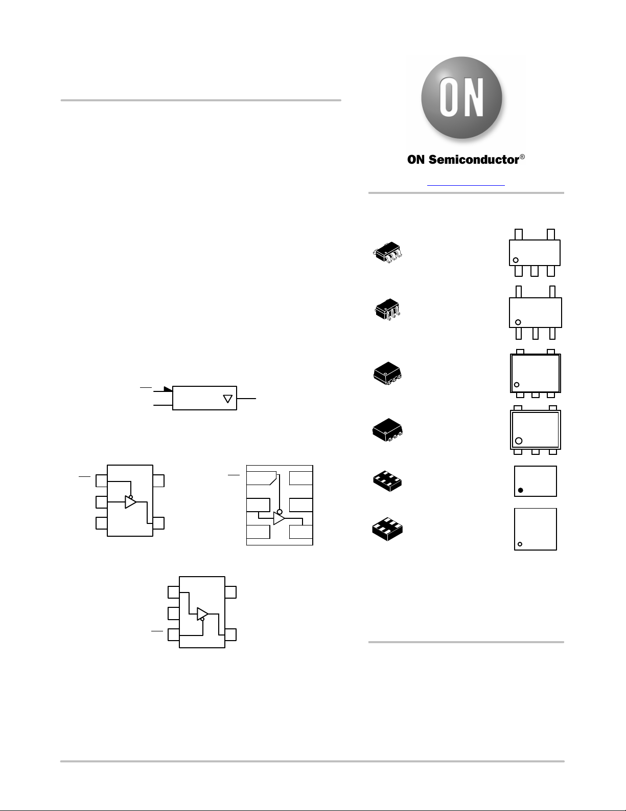
OE
A
EN
Figure 1. Logic Symbol
Y
www.onsemi.com
SC−74A
CASE 318BQ
SC−88A
(SC−70−5/SOT−353)
CASE 419A−02
SOT−553, 5 LEAD
CASE 463B
SOT−953
CASE 527AE
MARKING
DIAGRAMS
XXX MG
G
XXXMG
G
XXMG
G
XM
5
OE
1
2
A
34
(SC−88A / SOT−553 /
SC−74A)
V
CC
YGND
A
1
2
GND
34
SOT−953
Figure 2. Pinout (Top View)
© Semiconductor Components Industries, LLC, 2019
February, 2021 − Rev. 1
OE
5
1
A
2
3
UDFN6
V
CC
YOE
V
6
CC
5
NC
YGND
4
*This information is generic. Please refer to device data
sheet for actual part marking. Pb−Free indicator, “G”
or microdot “G”, may or may not be present.
UDFN6, 1.45x1.0, 0.5P
CASE 517AQ
UDFN6, 1x1, 0.35P
CASE 517BX
X, XX = Specific Device Code
M = Date Code*
G = Pb−Free Package
(Note: Microdot may be in either location)
XM
X M
ORDERING INFORMATION
See detailed ordering, marking and shipping information in the
package dimensions section on page 7 of this data sheet.
1 Publication Order Number:
NL17SV125/D
Page 2
NL17SV125
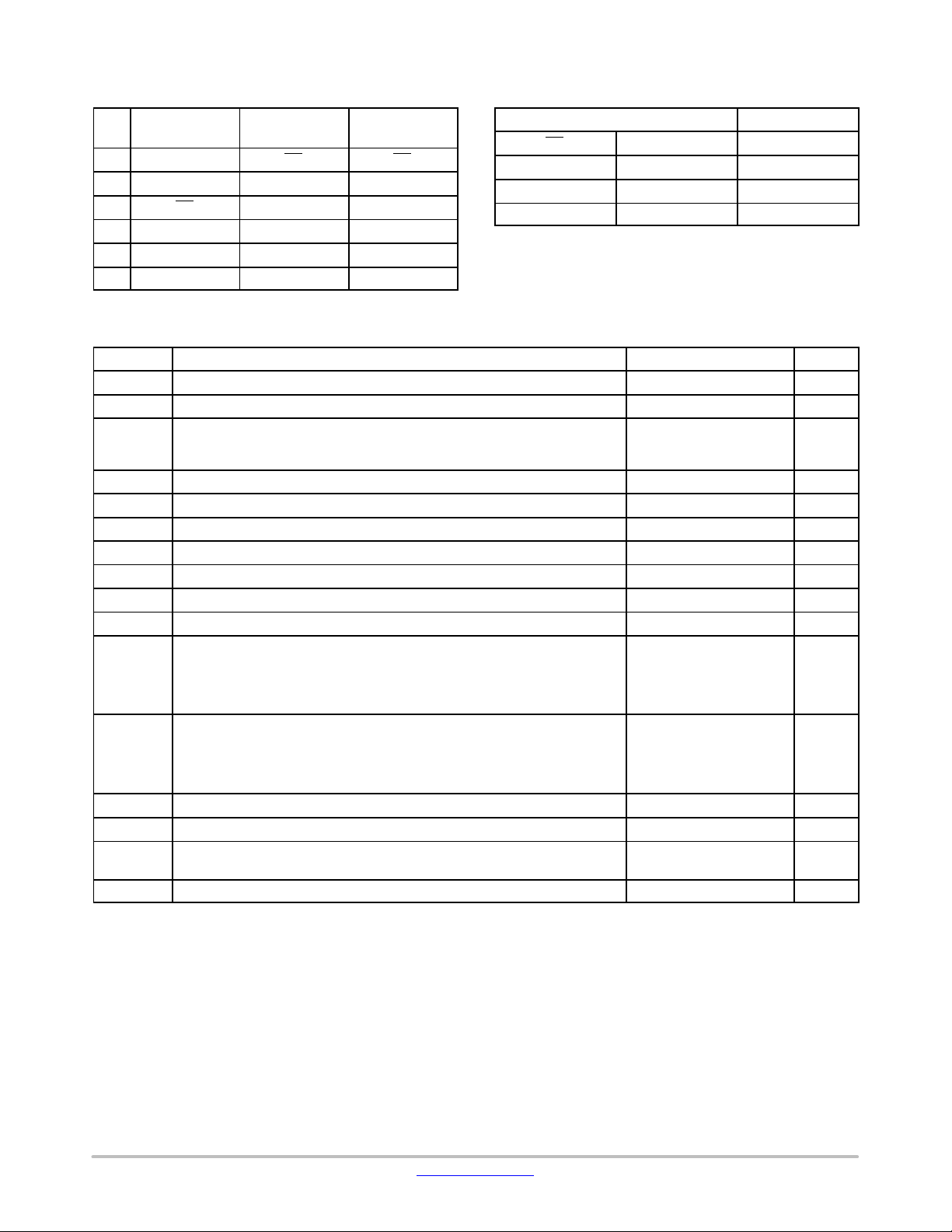
PIN ASSIGNMENT
SC88A / SOT553
Pin SOT−953
1 A OE OE
2 GND A A
3 OE GND GND
4 Y Y Y
5 V
CC
6 − − V
/ SC−74A
V
CC
UDFN6
NC
CC
FUNCTION TABLE
Input Output
OE A Y
L L L
L H H
H X Z
X = Don’t Care
Z = High Impedance State
MAXIMUM RATINGS
Symbol Characteristics Value Unit
V
CC
V
IN
V
OUT
I
IK
I
OK
I
OUT
ICC or I
T
STG
T
L
T
J
q
JA
P
D
MSL Moisture Sensitivity Level 1 −
F
R
V
ESD
I
Latchup
Stresses exceeding those listed in the Maximum Ratings table may damage the device. If any of these limits are exceeded, device functionality
should not be assumed, damage may occur and reliability may be affected.
1. Applicable to devices with outputs that may be tri−stated.
2. Measured with minimum pad spacing on an FR4 board, using 10 mm−by−1 inch, 2 ounce copper trace no air flow per JESD51−7.
3. HBM tested to EIA / JESD22−A114−A. CDM tested to JESD22−C101−A. JEDEC recommends that ESD qualification to EIA/JESD22−A115A
(Machine Model) be discontinued.
4. Tested to EIA/JESD78 Class II.
DC Supply Voltage −0.5 to +4.3 V
DC Input Voltage −0.5 to +4.3 V
DC Output Voltage Active−Mode (High or Low State)
Tri−State Mode (Note 1)
Power−Down Mode (V
CC
= 0 V)
−0.5 to VCC + 0.5
−0.5 to +4.3
−0.5 to +4.3
DC Input Diode Current VIN < GND −50 mA
DC Output Diode Current V
< GND −50 mA
OUT
DC Output Source/Sink Current ±50 mA
DC Supply Current per Supply Pin or Ground Pin ±50 mA
GND
Storage Temperature Range −65 to +150 °C
Lead Temperature, 1 mm from Case for 10 Seconds 260 °C
Junction Temperature Under Bias +150 °C
Thermal Resistance (Note 2) SC−88A
SOT−553
SOT−953
SC−74A
UDFN6
Power Dissipation in Still Air SC−88A
SOT−553
SOT−953
SC−74A
UDFN6
377
324
254
320
154
332
386
491
390
812
Flammability Rating Oxygen Index: 28 to 34 UL 94 V−0 @ 0.125 in −
ESD Withstand Voltage (Note 3) Human Body Model
Charged Device Model
2000
1000
Latchup Performance (Note 4) ±100 mA
V
°C/W
mW
V
www.onsemi.com
2
Page 3
NL17SV125
RECOMMENDED OPERATING CONDITIONS
Symbol Parameter Min Max Unit
V
CC
V
V
OUT
T
t
r
Functional operation above the stresses listed in the Recommended Operating Ranges is not implied. Extended exposure to stresses beyond
the Recommended Operating Ranges limits may affect device reliability.
DC ELECTRICAL CHARACTERISTICS
Symbol
V
IH
V
IL
V
OH
Positive DC Supply Voltage 0.9 3.6 V
DC Input Voltage 0 3.6
IN
DC Output Voltage Active−Mode (High or Low State)
Tri−State Mode (Note 1)
Power−Down Mode (V
Operating Temperature Range −55 +125 °C
A
, t
Input Transition Rise and Fall Time 0 20 ns/V
f
CC
= 0 V)
0
0
0
TA = 255C TA = −555C to +1255C
Parameter Condition V
High−Level Input
Voltage
(V)
CC
0.9 − 0.5 − − −
1.1 to 1.3 0.65 x V
1.4 to 1.6 0.65 x V
1.65 to 1.95 0.65 x V
Min Typ Max Min Max
− − 0.65 x V
CC
− − 0.65 x V
CC
− − 0.65 x V
CC
CC
CC
CC
2.3 to < 2.7 1.6 − − 1.6 −
2.0 − − 2.0 −
CC
CC
CC
− 0.35 x V
− 0.35 x V
− 0.35 x V
Low−Level Input
Voltage
2.7 to 3.6
0.9 − 0.5 − − −
1.1 to 1.3 − − 0.35 x V
1.4 to 1.6 − − 0.35 x V
1.65 to 1.95 − − 0.35 x V
2.3 to < 2.7 − − 0.7 − 0.7
2.7 to 3.6 − − 0.8 − 0.8
High−Level Output
Voltage
VIN = VIH or V
IOH = −100 mA
IL
0.9 − VCC –
− − −
0.1
1.1 to 1.3 VCC – 0.1 − − VCC – 0.1 −
1.4 to 1.6 VCC – 0.1 − − VCC – 0.1 −
1.65 to 1.95 VCC – 0.2 − − VCC – 0.2 −
2.3 to <2.7 VCC – 0.2 − − VCC – 0.2 −
2.7 to 3.6 VCC – 0.2 − − VCC – 0.2 −
IOH = −2 mA 1.1 to 1.3 0.75 x V
IOH = −4 mA 1.4 to 1.6 0.75 x V
IOH = −6 mA
1.65 to 1.95 1.25 − − 1.25 −
− − 0.75 x V
CC
− − 0.75 x V
CC
CC
CC
2.3 to 2.7 2.0 − − 2.0 −
IOH = −12 mA
2.3 to 2.7 1.8 − − 1.8 −
2.7 to 3.6 2.2 − − 2.2 −
IOH = −18 mA
2.3 to 2.7 1.7 − − 1.7 −
2.7 to 3.6 2.4 − − 2.4 −
IOH = −24 mA 2.7 to 3.6 2.2 − − 2.2 −
V
3.6
3.6
V
CC
Unit
V
−
−
−
V
CC
CC
CC
V
−
−
www.onsemi.com
3
Page 4
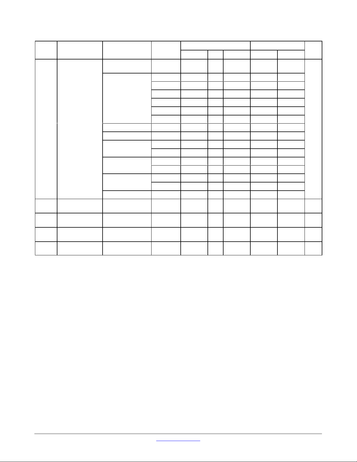
NL17SV125
DC ELECTRICAL CHARACTERISTICS (continued)
T
= −555C to +1255CTA = 255C
A
Symbol Unit
Low−Level Output
V
OL
Voltage
VIN = VIH or V
IL
IOL = 100 mA
V
(V)ConditionParameter
CC
0.9 − 0.1 − − −
1.1 to 1.3 − − 0.1 − 0.1
1.4 to 1.6 − − 0.1 − 0.1
1.65 to 1.95 − − 0.2 − 0.2
2.3 to < 2.7 − − 0.2 − 0.2
2.7 to 3.6 − − 0.2 − 0.2
IOL = 2 mA 1.1 to 1.3 − − 0.25 x V
IOL = 4 mA 1.4 to 1.6 − − 0.25 x V
IOL = 6 mA
1.65 to 1.95 − − 0.3 − 0.3
CC
CC
− 0.25 x V
− 0.25 x V
2.3 to 2.7 − − 0.3 − 0.3
IOL = 12 mA
2.3 to 2.7 − − 0.4 − 0.4
2.7 to 3.6 − − 0.4 − 0.4
IOL = 18 mA
2.3 to 2.7 − − 0.6 − 0.6
2.7 to 3.6 − − 0.4 − 0.4
IOL = 24 mA 2.7 to 3.6 − − 0.55 − 0.55
I
Input Leakage
IN
Current
I
3−State Output
OZ
Leakage Current
I
Power Off Leakage
OFF
Current
I
Quiescent Supply
CC
Current
VIN = 3.6 V or GND 0.9 to 3.6 − − ±0.1 − ±0.9
V
= 0 V to 3.6 V 0.9 to 3.6 − − ±0.5 − ±5.0
OUT
VIN = 3.6 V or
V
= 3.6 V
OUT
0 − − 1.0 − 5.0
VIN = VCC or GND 0.9 to 3.6 − − 0.9 − 5.0
Product parametric performance is indicated in the Electrical Characteristics for the listed test conditions, unless otherwise noted. Product
performance may not be indicated by the Electrical Characteristics if operated under different conditions.
MaxMinMaxTypMin
V
CC
CC
mA
mA
mA
mA
www.onsemi.com
4
Page 5

AC ELECTRICAL CHARACTERISTICS
Symbol
t
, t
PLH
t
, t
PZH
t
, t
PHZ
PHL
PZL
PLZ
Parameter
Propagation Delay,
A to Y (Figures 3 and 4)
Output Enable Time,
OE
to Y
(Figures 3 and 4)
Output Disable Time,
OE
to Y
(Figures 3 and 4)
R
= 1 MW, C
L
R
= 2 kW, C
L
R
= 500 W, C
L
C
= 30 pF
L
= RL = 1 kW
R
1
C
= 30 pF
L
= RL = 1 kW
R
1
NL17SV125
TA = 25°C
Min
Condition
= 15 pF
L
= 15 pF 1.10 to 1.30 − 7.3 11.5 − 14.9
L
VCC (V)
0.9 − 16.6 − − −
Typ
1.40 to 1.60 − 3.9 5.3 − 5.7
= 30 pF 1.65 to 1.95 − 2.7 4.3 − 4.6
L
2.3 to 2.7 − 1.9 2.8 − 3.0
2.7 to 3.6 − 1.6 2.6 − 2.8
0.9 − 14 − − −
1.10 to 1.30 − 6.0 9.7 − 16.4
1.40 to 1.60 − 4.0 6.0 − 7.5
1.65 to 1.95 − 3.0 4.5 − 5.0
2.3 to 2.7 − 2.0 3.0 − 3.4
2.7 to 3.6 − 1.2 2.6 − 2.9
0.9 − 14 − − −
1.10 to 1.30 − 5.0 9.5 − 14.0
1.40 to 1.60 − 3.0 5.5 − 7.0
1.65 to 1.95 − 2.0 5.6 − 5.8
2.3 to 2.7 − 1.5 4.2 − 5.0
2.7 to 3.6 − 1.0 3.9 − 4.2
TA = −555C to +1255C
Max
Min
Max
Unit
ns
ns
ns
CAPACITIVE CHARACTERISTICS
Symbol Parameter Test Condition Typical (TA = 25°C) Unit
C
C
C
5. CPD is defined as the value of the internal equivalent capacitance which is calculated from the operating current consumption without load.
Average operating current can be obtained by the equation I
power consumption: P
Input Capacitance VCC = 0 V 2.0 pF
IN
Output Capacitance VCC = 0 V 4.5 pF
OUT
Power Dissipation Capacitance (Note 5) 10 MHz, VCC = 0.9 to 3.6 V, VIN = 0 V or V
PD
= CPD VCC fin + ICC. CPD is used to determine the no−load dynamic
)
= CPD V
D
2
fin + ICC VCC.
CC
CC(OPR
CC
20 pF
www.onsemi.com
5
Page 6

NL17SV125
OPEN
2 x V
CC
R
INPUT
R
T
DUT
1
R
L
CL includes probe and jig capacitance
R
is Z
T
of pulse generator (typically 50 W)
OUT
f = 1 MHz
tr = 3 ns
90%
90%
INPUT
V
mi
V
10%
t
PHL
t
PLH
V
mo
V
mo
OUTPUT
OUTPUT
GND
t
PLH
t
t
PHZ
PLZ
Test
/ t
/ t
/ t
PHL
PZL
PZH
Switch Position
Open
2 x V
CC
GND
OUTPUT
CL*
Figure 3. Test Circuit
V
GND
VOL + V
V
V
VOH − V
~V
OL
OH
CC
CC
Y
Y
tf = 3 ns
V
CC
INPUT
mi
t
PLH
t
PHL
10%
V
V
mo
mo
GND
V
OH
V
OL
V
OH
OUTPUT
OUTPUT
t
t
PZH
PZL
V
mi
V
mo
V
mo
V
mi
t
PLZ
t
PHZ
V
OL
Vmo, V
VCC, V Vmi, V
0.9 V
1.1 to 1.3 V
1.4 to 1.6 V
1.65 to 1.95 V
2.3 to 2.7 V
/ 2 V
CC
/ 2 V
CC
/ 2 V
CC
/ 2 V
CC
/ 2 V
CC
, t
PLH
PHL
/ 2 V
CC
/ 2 V
CC
/ 2 V
CC
/ 2 V
CC
/ 2 V
CC
t
PZL
, t
, t
PLZ
, t
PZH
PHZ
/ 2 0.1
CC
/ 2 0.1
CC
/ 2 0.1
CC
/ 2 0.15
CC
/ 2 0.15
CC
t
3.0 to 3.6 1.5 1.5 1.5 0.3
Figure 4. Switching Waveforms
~0 V
VY, V
www.onsemi.com
6
Page 7

NL17SV125
ORDERING INFORMATION
Pin 1 Orientation
Device Package Marking
NL17SV125DFT2G
(Contact ON Semiconductor)
NLV17SV125DFT2G* SC−88A CC Q4 3000 / Tape & Reel
SC−88A CC Q4 3000 / Tape & Reel
(See below)
Shipping
†
NL17SV125XV5T2G
(Contact ON Semiconductor)
NL17SV125P5T5G
(Contact ON Semiconductor)
NL17SV125DBVT1G
(Contact ON Semiconductor)
NL17SV125MU1TCG
(Contact ON Semiconductor)
NL17SV125MU3TCG
(Contact ON Semiconductor)
†For information on tape and reel specifications, including part orientation and tape sizes, please refer to our Tape and Reel Packaging
Specifications Brochure, BRD8011/D.
*NLV Prefix for Automotive and Other Applications Requiring Unique Site and Control Change Requirements; AEC−Q100 Qualified and PPAP
Capable.
SOT−553 TBD Q4 4000 / Tape & Reel
SOT−953 TBD Q2 8000 / Tape & Reel
SC−74A TBD Q4 3000 / Tape & Reel
UDFN6, 1.45 x 1.0, 0.5P TBD Q4 3000 / Tape & Reel
UDFN6, 1.0 x 1.0, 0.35P TBD Q4 3000 / Tape & Reel
Pin 1 Orientation in Tape and Reel
www.onsemi.com
7
Page 8

54
E1
123
B
A
D
e
TOP VIEW
A
SIDE VIEW
RECOMMENDED
SOLDERING FOOTPRINT*
0.95
PITCH
5X
E
C
b
0.20
SEATING
PLANE
C AB
NL17SV125
PACKAGE DIMENSIONS
SC−74A
CASE 318BQ
ISSUE B
M
0.05
A1
L
DETAIL A
DETAIL A
c
END VIEW
NOTES:
1. DIMENSIONING AND TOLERANCING PER ASME
Y14.5M, 1994.
2. CONTROLLING DIMENSION: MILLIMETERS.
3. MAXIMUM LEAD THICKNESS INCLUDES LEAD FINISH
THICKNESS. MINIMUM LEAD THICKNESS IS THE
MINIMUM THICKNESS OF BASE MATERIAL.
4. DIMENSIONS A AND B DO NOT INCLUDE MOLD
FLASH, PROTRUSIONS, OR GATE BURRS. MOLD
FLASH, PROTRUSIONS, OR GATE BURRS SHALL NOT
EXCEED 0.15 PER SIDE.
MILLIMETERS
DIM MIN MAX
A 0.90 1.10
A1 0.01 0.10
b 0.25 0.50
c 0.10 0.26
D
2.85 3.15
E 2.50 3.00
E1
1.35 1.65
e 0.95 BSC
L 0.20 0.60
M 0 10
__
2.40
5X
1.00
5X
0.70
DIMENSIONS: MILLIMETERS
*For additional information on our Pb−Free strategy and soldering
details, please download the ON Semiconductor Soldering and
Mounting Techniques Reference Manual, SOLDERRM/D.
www.onsemi.com
8
Page 9

NL17SV125
PACKAGE DIMENSIONS
SC−88A (SC−70−5/SOT−353)
CASE 419A−02
ISSUE L
A
G
45
D
5 PL
−B−
MM
B0.2 (0.008)
S
12 3
N
NOTES:
1. DIMENSIONING AND TOLERANCING
PER ANSI Y14.5M, 1982.
2. CONTROLLING DIMENSION: INCH.
3. 419A−01 OBSOLETE. NEW STANDARD
419A−02.
4. DIMENSIONS A AND B DO NOT INCLUDE
MOLD FLASH, PROTRUSIONS, OR GATE
BURRS.
INCHES
DIMAMIN MAX MIN MAX
B 1.15 1.350.045 0.053
C 0.80 1.100.031 0.043
D 0.10 0.300.004 0.012
G 0.65 BSC0.026 BSC
H --- 0.10---0.004
J 0.10 0.250.004 0.010
K 0.10 0.300.004 0.012
N 0.20 REF0.008 REF
S 2.00 2.200.079 0.087
MILLIMETERS
1.80 2.200.071 0.087
J
C
H
K
SOLDER FOOTPRINT
0.50
0.0197
0.40
0.0157
STYLE 1:
PIN 1. BASE
2. EMITTER
3. BASE
4. COLLECTOR
5. COLLECTOR
STYLE 6:
PIN 1. EMITTER 2
2. BASE 2
3. EMITTER 1
4. COLLECTOR
5. COLLECTOR 2/BASE 1
1.9
0.0748
STYLE 2:
PIN 1. ANODE
2. EMITTER
3. BASE
4. COLLECTOR
5. CATHODE
STYLE 7:
PIN 1. BASE
2. EMITTER
3. BASE
4. COLLECTOR
5. COLLECTOR
SCALE 20:1
STYLE 3:
PIN 1. ANODE 1
2. N/C
3. ANODE 2
4. CATHODE 2
5. CATHODE 1
STYLE 8:
PIN 1. CATHODE
2. COLLECTOR
3. N/C
4. BASE
5. EMITTER
0.65
0.025
0.65
0.025
mm
ǒ
inches
Ǔ
STYLE 4:
PIN 1. SOURCE 1
2. DRAIN 1/2
3. SOURCE 1
4. GATE 1
5. GATE 2
STYLE 9:
PIN 1. ANODE
2. CATHODE
3. ANODE
4. ANODE
5. ANODE
STYLE 5:
PIN 1. CATHODE
2. COMMON ANODE
3. CATHODE 2
4. CATHODE 3
5. CATHODE 4
www.onsemi.com
9
Page 10

NL17SV125
PACKAGE DIMENSIONS
SOT−553, 5 LEAD
CASE 463B
ISSUE C
D
−X−
45
12 3
e
E
−Y−
5 PL
b
0.08 (0.003) X
M
Y
A
L
H
E
c
RECOMMENDED
SOLDERING FOOTPRINT*
0.3
0.0118
0.45
0.0177
1.0
1.35
0.0531
*For additional information on our Pb−Free strategy and soldering
details, please download the ON Semiconductor Soldering and
Mounting Techniques Reference Manual, SOLDERRM/D.
0.0394
0.5
0.0197
0.5
0.0197
SCALE 20:1
ǒ
inches
mm
Ǔ
NOTES:
1. DIMENSIONING AND TOLERANCING PER ANSI Y14.5M, 1982.
2. CONTROLLING DIMENSION: MILLIMETERS
3. MAXIMUM LEAD THICKNESS INCLUDES LEAD FINISH
THICKNESS. MINIMUM LEAD THICKNESS IS THE MINIMUM
THICKNESS OF BASE MATERIAL.
DIMAMIN NOM MAX MIN
b 0.17 0.22 0.27 0.007
c
D 1.55 1.60 1.65 0.061
E 1.15 1.20 1.25 0.045
e 0.50 BSC
L 0.10 0.20 0.30 0.004
H
E
MILLIMETERS
0.50 0.55 0.60 0.020
0.08 0.13 0.18
1.55 1.60 1.65 0.061 0.063 0.065
INCHES
NOM MAX
0.022 0.024
0.009 0.011
0.003 0.005 0.007
0.063 0.065
0.047 0.049
0.020 BSC
0.008 0.012
STYLE 1:
PIN 1. BASE
2. EMITTER
3. BASE
4. COLLECTOR
5. COLLECTOR
STYLE 6:
PIN 1. EMITTER 2
2. BASE 2
3. EMITTER 1
4. COLLECTOR 1
5. COLLECTOR 2/BASE 1
STYLE 2:
PIN 1. CATHODE
2. COMMON ANODE
3. CATHODE 2
4. CATHODE 3
5. CATHODE 4
STYLE 7:
PIN 1. BASE
2. EMITTER
3. BASE
4. COLLECTOR
5. COLLECTOR
STYLE 3:
PIN 1. ANODE 1
2. N/C
3. ANODE 2
4. CATHODE 2
5. CATHODE 1
STYLE 8:
PIN 1. CATHODE
2. COLLECTOR
3. N/C
4. BASE
5. EMITTER
www.onsemi.com
10
STYLE 4:
PIN 1. SOURCE 1
2. DRAIN 1/2
3. SOURCE 1
4. GATE 1
5. GATE 2
STYLE 9:
PIN 1. ANODE
2. CATHODE
3. ANODE
4. ANODE
5. ANODE
STYLE 5:
PIN 1. ANODE
2. EMITTER
3. BASE
4. COLLECTOR
5. CATHODE
Page 11

NL17SV125
PACKAGE DIMENSIONS
UDFN6, 1.45x1.0, 0.5P
CASE 517AQ
ISSUE O
REFERENCE
6X
PIN ONE
0.10 C
0.10
0.05 C
0.05 C
DETAIL A
TOP VIEW
C
SIDE VIEW
e
1
BOTTOM VIEW
D
DETAIL B
A1
3
46
A
B
E
A
A2
C
L6X
b
6X
0.10 B
0.05ACC
L1
SEATING
PLANE
NOTE 3
L
DETAIL A
OPTIONAL
CONSTRUCTIONS
MOLD CMPDEXPOSED Cu
DETAIL B
OPTIONAL
CONSTRUCTIONS
L
NOTES:
1. DIMENSIONING AND TOLERANCING PER
ASME Y14.5M, 1994.
2. CONTROLLING DIMENSION: MILLIMETERS.
3. DIMENSION b APPLIES TO PLATED TERMINAL
AND IS MEASURED BETWEEN 0.15 AND
0.30 mm FROM THE TERMINAL TIP.
MILLIMETERS
DIM MIN MAX
A 0.45 0.55
A1 0.00 0.05
A2 0.07 REF
b 0.20 0.30
D 1.45 BSC
E 1.00 BSC
e 0.50 BSC
L 0.30 0.40
L1 −−− 0.15
MOUNTING FOOTPRINT
6X
PACKAGE
OUTLINE
0.30
1.24
6X
0.53
1
0.50
PITCH
DIMENSIONS: MILLIMETERS
*For additional information on our Pb−Free strategy and soldering
details, please download the ON Semiconductor Soldering and
Mounting Techniques Reference Manual, SOLDERRM/D.
www.onsemi.com
11
Page 12

NL17SV125
PACKAGE DIMENSIONS
UDFN6, 1x1, 0.35P
CASE 517BX
ISSUE O
PIN ONE
REFERENCE
2X
2X
0.10 C
0.10
0.05 C
0.05 C
C
TOP VIEW
SIDE VIEW
e
1
L1
BOTTOM VIEW
D
A B
E
A3
A
A1
C
SEATING
PLANE
NOTES:
1. DIMENSIONING AND TOLERANCING PER
ASME Y14.5M, 1994.
2. CONTROLLING DIMENSION: MILLIMETERS.
3. DIMENSION b APPLIES TO PLATED
TERMINAL AND IS MEASURED BETWEEN
0.15 AND 0.20 MM FROM TERMINAL TIP.
4. PACKAGE DIMENSIONS EXCLUSIVE OF
BURRS AND MOLD FLASH.
MILLIMETERS
DIM MIN MAX
A 0.45 0.55
A1 0.00 0.05
A3 0.13 REF
b 0.12 0.22
D 1.00 BSC
E 1.00 BSC
e 0.35 BSC
L 0.25 0.35
L1 0.30 0.40
L5X
3
46
b
6X
0.10 B
0.05ACC
M
M
NOTE 3
RECOMMENDED
SOLDERING FOOTPRINT*
5X
0.48
PKG
OUTLINE
1
DIMENSIONS: MILLIMETERS
0.53
*For additional information on our Pb−Free strategy and soldering
details, please download the ON Semiconductor Soldering and
Mounting Techniques Reference Manual, SOLDERRM/D.
6X
0.22
1.18
0.35
PITCH
www.onsemi.com
12
Page 13

NL17SV125
PACKAGE DIMENSIONS
SOT−953
CASE 527AE
ISSUE E
D
PIN ONE
INDICATOR
123
TOP VIEW
5X
L3
5X
L2
BOTTOM VIEW
SOLDERING FOOTPRINT*
5X
0.20
X
Y
A
45
E
H
E
C
SIDE VIEW
e
5X
L
5X
b
NOTES:
1. DIMENSIONING AND TOLERANCING PER ASME
Y14.5M, 1994.
2. CONTROLLING DIMENSION: MILLIMETERS
3. MAXIMUM LEAD THICKNESS INCLUDES LEAD
FINISH. MINIMUM LEAD THICKNESS IS THE
MINIMUM THICKNESS OF THE BASE MATERIAL.
4. DIMENSIONS D AND E DO NOT INCLUDE MOLD
FLASH, PROTRUSIONS, OR GATE BURRS.
MILLIMETERS
DIM MIN NOM MAX
A 0.34 0.37 0.40
b 0.10 0.15 0.20
C 0.07 0.12 0.17
D 0.95 1.00 1.05
E 0.75 0.80 0.85
e 0.35 BSC
H
E
0.95 1.00 1.05
L
L2 0.05 0.10 0.15
L3 −−− −−− 0.15
0.175 REF
X0.08 Y
5X
0.35
PACKAGE
OUTLINE
1.20
1
0.35
PITCH
DIMENSIONS: MILLIMETERS
*For additional information on our Pb−Free strategy and soldering
details, please download the ON Semiconductor Soldering and
Mounting Techniques Reference Manual, SOLDERRM/D.
ON Semiconductor and are trademarks of Semiconductor Components Industries, LLC dba ON Semiconductor or its subsidiaries in the United States and/or other countries.
ON Semiconductor owns the rights to a number of patents, trademarks, copyrights, trade secrets, and other intellectual property. A listing of ON Semiconductor’s product/patent
coverage may be accessed at www.onsemi.com/site/pdf/Patent−Marking.pdf
ON Semiconductor makes no warranty, representation or guarantee regarding the suitability of its products for any particular purpose, nor does ON Semiconductor assume any liability
arising out of the application or use of any product or circuit, and specifically disclaims any and all liability, including without limitation special, consequential or incidental damages.
Buyer is responsible for its products and applications using ON Semiconductor products, including compliance with all laws, regulations and safety requirements or standards,
regardless of any support or applications information provided by ON Semiconductor. “Typical” parameters which may be provided in ON Semiconductor data sheets and/or
specifications can and do vary in different applications and actual performance may vary over time. All operating parameters, including “Typicals” must be validated for each customer
application by customer’s technical experts. ON Semiconductor does not convey any license under its patent rights nor the rights of others. ON Semiconductor products are not
designed, intended, or authorized for use as a critical component in life support systems or any FDA Class 3 medical devices or medical devices with a same or similar classification
in a foreign jurisdiction or any devices intended for implantation in the human body. Should Buyer purchase or use ON Semiconductor products for any such unintended or unauthorized
application, Buyer shall indemnify and hold ON Semiconductor and its officers, employees, subsidiaries, affiliates, and distributors harmless against all claims, costs, damages, and
expenses, and reasonable attorney fees arising out of, directly or indirectly, any claim of personal injury or death associated with such unintended or unauthorized use, even if such
claim alleges that ON Semiconductor was negligent regarding the design or manufacture of the part. ON Semiconductor is an Equal Opportunity/Affirmative Action Employer. This
literature is subject to all applicable copyright laws and is not for resale in any manner.
. ON Semiconductor reserves the right to make changes without further notice to any products herein.
PUBLICATION ORDERING INFORMATION
LITERATURE FULFILLMENT:
Email Requests to: orderlit@onsemi.com
ON Semiconductor Website: www.onsemi.com
TECHNICAL SUPPORT
North American Technical Support:
Voice Mail: 1 800−282−9855 Toll Free USA/Canada
Phone: 011 421 33 790 2910
Europe, Middle East and Africa Technical Support:
Phone: 00421 33 790 2910
For additional information, please contact your local Sales Representative
◊
www.onsemi.com
13
 Loading...