

Page 1
NL17SG08
Single 2-Input AND Gate
The NL17SG08 MiniGatet is an advanced high−speed CMOS
2−input AND gate in ultra−small footprint.
The NL17SG08 input structures provides protection when voltages
up to 4.6 V are applied.
Features
• Wide Operating V
• High Speed: t
• Low Power Dissipation: I
• 4.6 V Overvoltage Tolerant (OVT) Input Pins
• Ultra−Small Packages
• NLV Prefix for Automotive and Other Applications Requiring
Unique Site and Control Change Requirements; AEC−Q101
Qualified and PPAP Capable
• These are Pb−Free and Halide−Free Devices
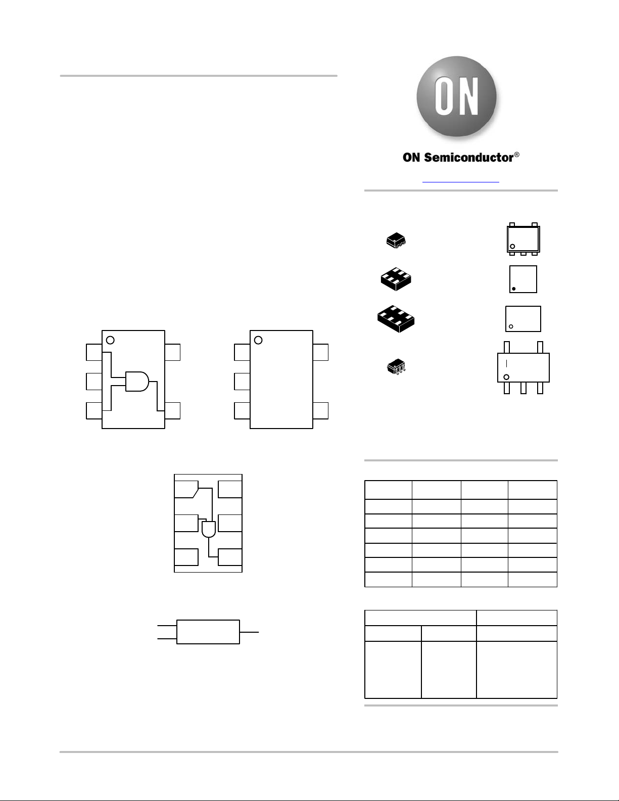
IN A
1
GND
2
Range: 0.9 V to 3.6 V
CC
= 2.5 ns (Typ) at VCC = 3.0 V, CL = 15 pF
PD
= 0.5 mA (Max) at TA = 25°C
CC
5
V
CC
IN B
IN A
1
2
www.onsemi.com
MARKING
DIAGRAMS
SOT−953
CASE 527AE
UDFN6
1.0 x 1.0
CASE 517BX
UDFN6
1.45 x 1.0
CASE 517AQ
5
V
CC
SC−88A
DF SUFFIX
CASE 419A
Y M
1
L
M
L
M
M
AT M G
G
IN B OUT Y
3
4
Figure 1. SOT−953
(Top Thru View)
IN B
1
IN A
2
GND
3
Figure 1. UDFN6
(Top View)
IN A
IN B
Figure 2. Logic Symbol
GND OUT Y
3
4
Figure 1. SC−88A
(Top View)
6
V
CC
NC
5
OUT Y
4
&
OUT Y
M = Date Code*
G = Pb−Free Package
(Note: Microdot may be in either location)
*Date Code orientation and/or position may vary
depending upon manufacturing location.
PIN ASSIGNMENT
PIN
1
2
3 IN B
4
5V
6−
SOT−953
IN A
GND
OUT Y
CC
SC−88A
IN B
IN A
GND
OUT Y
V
CC
−
UDFN6
IN B
IN A
GND
OUT Y
VC
V
CC
FUNCTION TABLE
Inputs Output
AB
L
L
H
H
L
H
L
H
Y
L
L
L
H
© Semiconductor Components Industries, LLC, 2016
June, 2016 − Rev. 7
See detailed ordering and shipping information in the package
ORDERING INFORMATION
dimensions section on page 5 of this data sheet.
1 Publication Order Number:
NL17SG08/D
Page 2
NL17SG08
MAXIMUM RATINGS
Symbol Parameter Value Unit
V
CC
V
V
OUT
I
IK
I
OK
I
OUT
I
CC
I
GND
T
STG
T
T
MSL Moisture Sensitivity Level 1
F
V
ESD
Stresses exceeding those listed in the Maximum Ratings table may damage the device. If any of these limits are exceeded, device functionality
should not be assumed, damage may occur and reliability may be affected.
1. Measured with minimum pad spacing on an FR4 board, using 10 mm−by−1 inch, 2−ounce copper trace with no air flow.
2. Tested to EIA/JESD22−A114−A.
3. Tested to EIA/JESD22−A115−A.
DC Supply Voltage −0.5 to +5.5 V
DC Input Voltage −0.5 to +4.6 V
IN
DC Output Voltage Output at High or Low State
Power−Down Mode (V
CC
= 0 V)
−0.5 to V
−0.5 to +4.6
CC
DC Input Diode Current VIN < GND −20 mA
DC Output Diode Current V
< GND −20 mA
OUT
DC Output Source/Sink Current ±20 mA
DC Supply Current per Supply Pin ±20 mA
DC Ground Current per Ground Pin ±20 mA
Storage Temperature Range −65 to +150 °C
Lead Temperature, 1 mm from Case for 10 Seconds 260 °C
L
Junction Temperature Under Bias +150 °C
J
Flammability Rating Oxygen Index: 28 to 34 UL 94 V−0 @ 0.125 in
R
ESD Withstand Voltage Human Body Model (Note 2)
Machine Model (Note 3)
>2000
>100
+0.5
V
V
RECOMMENDED OPERATING CONDITIONS
Symbol Characteristics Min Max Unit
V
CC
V
V
OUT
T
Dt / DV
Functional operation above the stresses listed in the Recommended Operating Ranges is not implied. Extended exposure to stresses beyond
the Recommended Operating Ranges limits may affect device reliability.
Positive DC Supply Voltage 0.9 3.6 V
Digital Input Voltage 0.0 3.6 V
IN
Output Voltage Output at High or Low State
Power−Down Mode (V
Operating Temperature Range −55 +125 °C
A
CC
= 0 V)
0.0
0.0
Input Transition Rise or Fail Rate VCC = 3.3 V ± 0.3 V 0 10 ns/V
V
3.6
CC
V
www.onsemi.com
2
Page 3
NL17SG08
DC ELECTRICAL CHARACTERISTICS
Symbol Parameter Conditions VCC (V)
V
V
V
OH
V
OL
I
IN
IH
IL
High-Level Input
Voltage
Low-Level Input
Voltage
High-Level
Output Voltage
Low-Level
Output Voltage
Input Leakage
Current
0.9 V
1.1 to 1.3 0.7xV
1.4 to 1.6 0.65xV
1.65 to 1.95 0.65xV
2.3 to 2.7 1.7 1.7
3.0 to 3.6 2.0 2.0
0.9 GND GND
1.1 to 1.3 0.3xV
1.4 to 1.6 0.35xV
1.65 to 1.95 0.35xV
2.3 to 2.7 0.7 0.7
3.0 to 3.6 0.8 0.8
VIN =
V
IH
V
IOH = −20 mA
or
IOH = -0.3 mA 1.1 to 1.3 0.75xV
IL
0.9 0.75 0.75
IOH = -1.7 mA 1.4 to 1.6 0.75xV
IOH = -3.0 mA 1.65 to 1.95 Vcc-0.45 Vcc-0.45
IOH = -4.0 mA 2.3 to 2.7 2.0 2.0
IOH = -8.0 mA 3.0 to 3.6 2.48 2.48
VIN =
V
IH
V
IOL = 20 mA
or
IOL = 1.1 mA 1.1 to 1.3 0.25xV
IL
0.9 0.1 0.1
IOL = 1.7 mA 1.4 to 1.6 0.25xV
IOL = 3.0 mA 1.65 to 1.95 0.45 0.45
IOL = 4.0 mA 2.3 to 2.7 0.4 0.4
IOL = 8.0 mA 3.0 to 3.6 0.4 0.4
0 ≤ VIN ≤ 3.6 V 0 to 3.6 $0.1 $1.0
TA = 255C
TA =
-555C to +1255C
Min Max Min Max
CC
CC
CC
CC
CC
CC
CC
CC
CC
CC
CC
V
CC
0.7xV
0.65xV
0.65xV
0.75xV
0.75xV
CC
CC
CC
0.3xV
0.35xV
0.35xV
CC
CC
0.25xV
0.25xV
Unit
V
V
CC
CC
CC
V
V
CC
CC
mA
I
CC
Quiescent
Supply Current
VIN = VCC or GND 3.6 0.5 10.0
mA
Product parametric performance is indicated in the Electrical Characteristics for the listed test conditions, unless otherwise noted. Product
performance may not be indicated by the Electrical Characteristics if operated under different conditions.
www.onsemi.com
3
Page 4
NL17SG08
AC ELECTRICAL CHARACTERISTICS (Input t
Symbol Parameter Test Condition VCC (V)
r
= t
= 3.0 ns)
f
TA = 255 C
TA =
-555C to +1255C
Min Typ Max Min Max Unit
t
,
PLH
t
PHL
Propagation Delay,
A or B to Y
CL = 10 pF,
= 1 MW
R
L
0.9 - 10.0 12.4 - 14.8
1.1 to 1.3 - 8.0 10.7 - 13.6
ns
1.4 to 1.6 - 5.9 9.6 - 11.3
1.65 to 1.95 - 4.5 7.0 - 7.5
2.3 to 2.7 - 2.9 4.4 - 4.9
3.0 to 3.6 - 2.2 3.5 - 4.1
CL = 15 pF,
= 1 MW
R
L
0.9 - 11.7 13.5 - 15.0
1.1 to 1.3 - 8.8 10.2 - 13.7
ns
1.4 to 1.6 - 6.5 9.5 - 12.6
1.65 to 1.95 - 5.0 7.7 - 8.0
2.3 to 2.7 - 3.2 4.9 - 5.6
3.0 to 3.6 - 2.5 3.8 - 4.4
CL = 30 pF,
= 1 MW
R
L
0.9 - 13.0 16.0 - 19.0
1.1 to 1.3 - 10.0 12.4 - 17.2
ns
1.4 to 1.6 - 8.9 11.8 - 14.9
1.65 to 1.95 - 6.9 10.3 - 10.8
2.3 to 2.7 - 4.4 6.4 - 6.8
3.0 to 3.6 - 3.5 4.9 - 5.4
C
IN
C
PD
Input Capacitance 0 to 3.6 3 - - - pF
Power Dissipation
Capacitance (Note 4)
f = 10 MHz 0.9 to 3.6 - 4 - - - pF
Product parametric performance is indicated in the Electrical Characteristics for the listed test conditions, unless otherwise noted. Product
performance may not be indicated by the Electrical Characteristics if operated under different conditions.
is defined as the value of the internal equivalent capacitance which is calculated from the operating current consumption without load.
4. C
PD
Average operating current can be obtained by the equation: I
power consumption; P
= CPD V
D
2
fin + ICC VCC.
CC
= CPD VCC fin + ICC. CPD is used to determine the no−load dynamic
)
CC(OPR
www.onsemi.com
4
Page 5

NL17SG08
Input A or B
Output Y
50%
t
PLH
50% V
Figure 2. Switching Waveforms
V
CC
INPUT
*Includes all probe and jig capacitance.
A 1−MHz square input wave is recommended
for propagation delay tests.
Figure 3. Test Circuit
CC
C
L*
50% V
CC
GND
t
PHL
V
V
OUTPUT
OH
OL
ORDERING INFORMATION
Device Package Shipping
NL17SG08P5T5G SOT−953
8000 / Tape & Reel
(Pb−Free)
NL17SG08DFT2G SC−88A
3000 / Tape & Reel
(Pb−Free)
NLV17SG08DFT2G* SC−88A
3000 / Tape & Reel
(Pb−Free)
NL17SG08AMUTCG UDFN6 1.45x1 mm
3000 / Tape & Reel
(Pb−Free)
NL17SG08CMUTCG UDFN6 1x1 mm
3000 / Tape & Reel
(Pb−Free)
†For information on tape and reel specifications, including part orientation and tape sizes, please refer to our Tape and Reel Packaging
Specifications Brochure, BRD8011/D.
*NLV Prefix for Automotive and Other Applications Requiring Unique Site and Control Change Requirements; AEC−Q101 Qualified and PPAP
Capable.
†
MiniGate is a trademark of Semiconductor Components Industries, LLC (SCILLC).
www.onsemi.com
5
Page 6

MECHANICAL CASE OUTLINE
PACKAGE DIMENSIONS
SC−88A (SC−70−5/SOT−353)
SCALE 2:1
CASE 419A−02
ISSUE L
DATE 17 JAN 2013
S
0.40
0.0157
A
G
45
12 3
D
5 PL
C
H
SOLDER FOOTPRINT
0.50
0.0197
−B−
MM
B0.2 (0.008)
N
K
0.65
0.025
0.65
0.025
NOTES:
1. DIMENSIONING AND TOLERANCING
PER ANSI Y14.5M, 1982.
2. CONTROLLING DIMENSION: INCH.
3. 419A−01 OBSOLETE. NEW STANDARD
419A−02.
4. DIMENSIONS A AND B DO NOT INCLUDE
MOLD FLASH, PROTRUSIONS, OR GATE
BURRS.
INCHES
DIMAMIN MAX MIN MAX
B 1.15 1.350.045 0.053
C 0.80 1.100.031 0.043
D 0.10 0.300.004 0.012
G 0.65 BSC0.026 BSC
H --- 0.10---0.004
J 0.10 0.250.004 0.010
K 0.10 0.300.004 0.012
N 0.20 REF0.008 REF
S 2.00 2.200.079 0.087
MILLIMETERS
1.80 2.200.071 0.087
J
GENERIC MARKING
DIAGRAM*
XXXMG
G
XXX = Specific Device Code
M = Date Code
G = Pb−Free Package
(Note: Microdot may be in either location)
*This information is generic. Please refer to
device data sheet for actual part marking.
Pb−Free indicator, “G” or microdot “G”, may
or may not be present. Some products may
not follow the Generic Marking.
1.9
0.0748
STYLE 1:
PIN 1. BASE
2. EMITTER
3. BASE
4. COLLECTOR
5. COLLECTOR
STYLE 6:
PIN 1. EMITTER 2
2. BASE 2
3. EMITTER 1
4. COLLECTOR
5. COLLECTOR 2/BASE 1
DOCUMENT NUMBER:
DESCRIPTION:
ON Semiconductor and are trademarks of Semiconductor Components Industries, LLC dba ON Semiconductor or its subsidiaries in the United States and/or other countries.
ON Semiconductor reserves the right to make changes without further notice to any products herein. ON Semiconductor makes no warranty, representation or guarantee regarding
the suitability of its products for any particular purpose, nor does ON Semiconductor assume any liability arising out of the application or use of any product or circuit, and specifically
disclaims any and all liability, including without limitation special, consequential or incidental damages. ON Semiconductor does not convey any license under its patent rights nor the
rights of others.
© Semiconductor Components Industries, LLC, 2018
STYLE 2:
PIN 1. ANODE
2. EMITTER
3. BASE
4. COLLECTOR
5. CATHODE
STYLE 7:
PIN 1. BASE
2. EMITTER
3. BASE
4. COLLECTOR
5. COLLECTOR
98ASB42984B
SC−88A (SC−70−5/SOT−353)
SCALE 20:1
STYLE 3:
PIN 1. ANODE 1
STYLE 8:
PIN 1. CATHODE
mm
ǒ
Ǔ
inches
STYLE 4:
2. N/C
3. ANODE 2
4. CATHODE 2
5. CATHODE 1
2. COLLECTOR
3. N/C
4. BASE
5. EMITTER
Electronic versions are uncontrolled except when accessed directly from the Document Repository.
Printed versions are uncontrolled except when stamped “CONTROLLED COPY” in red.
PIN 1. SOURCE 1
2. DRAIN 1/2
3. SOURCE 1
4. GATE 1
5. GATE 2
STYLE 9:
PIN 1. ANODE
2. CATHODE
3. ANODE
4. ANODE
5. ANODE
STYLE 5:
PIN 1. CATHODE
2. COMMON ANODE
3. CATHODE 2
4. CATHODE 3
5. CATHODE 4
Note: Please refer to datasheet for
style callout. If style type is not called
out in the datasheet refer to the device
datasheet pinout or pin assignment.
PAGE 1 OF 1
www.onsemi.com
Page 7

MECHANICAL CASE OUTLINE
PACKAGE DIMENSIONS
1
SCALE 4:1
UDFN6, 1.45x1.0, 0.5P
CASE 517AQ−01
ISSUE O
DATE 15 MAY 2008
REFERENCE
6X
PIN ONE
0.10 C
0.10 C
0.05 C
0.05 C
DETAIL A
D
TOP VIEW
DETAIL B
SIDE VIEW
e
1
BOTTOM VIEW
A
B
L1
E
A
L
DETAIL A
OPTIONAL
CONSTRUCTIONS
MOLD CMPDEXPOSED Cu
DETAIL B
OPTIONAL
CONSTRUCTIONS
L
NOTES:
1. DIMENSIONING AND TOLERANCING PER
ASME Y14.5M, 1994.
2. CONTROLLING DIMENSION: MILLIMETERS.
3. DIMENSION b APPLIES TO PLATED TERMINAL
AND IS MEASURED BETWEEN 0.15 AND
0.30 mm FROM THE TERMINAL TIP.
MILLIMETERS
DIM MIN MAX
A 0.45 0.55
A1 0.00 0.05
A2 0.07 REF
b 0.20 0.30
D 1.45 BSC
E 1.00 BSC
e 0.50 BSC
L 0.30 0.40
L1 −−− 0.15
GENERIC
A1
A2
C
SEATING
PLANE
L6X
3
46
b
6X
0.10 B
NOTE 3
0.05ACC
MARKING DIAGRAM*
XM
X = Specific Device Code
M = Date Code
*This information is generic. Please refer to
device data sheet for actual part marking.
Pb−Free indicator, “G” or microdot “ G”,
may or may not be present.
MOUNTING FOOTPRINT
6X
PACKAGE
OUTLINE
6X
0.53
1
*For additional information on our Pb−Free strategy and soldering
details, please download the ON Semiconductor Soldering and
Mounting Techniques Reference Manual, SOLDERRM/D.
DOCUMENT NUMBER:
STATUS:
NEW STANDARD:
© Semiconductor Components Industries, LLC, 2002
October, 2002 − Rev. 0
DESCRIPTION:
0.30
1.24
0.50
PITCH
DIMENSIONS: MILLIMETERS
98AON30313E
ON SEMICONDUCTOR STANDARD
http://onsemi.com
UDFN6, 1.45X1.0, 0.5P
Electronic versions are uncontrolled except when
accessed directly from the Document Repository. Printed
versions are uncontrolled except when stamped
“CONTROLLED COPY” in red.
Case Outline Number:
1
PAGE 1 OF 2
XXX
Page 8

DOCUMENT NUMBER:
98AON30313E
PAGE 2 OF 2
ISSUE REVISION DATE
O RELEASED FOR PRODUCTION. REQ. BY K. VAN TYNE. 15 MAY 2008
ON Semiconductor and are registered trademarks of Semiconductor Components Industries, LLC (SCILLC). SCILLC reserves the right to make changes without further notice
to any products herein. SCILLC makes no warranty, representation or guarantee regarding the suitability of its products for any particular purpose, nor does SCILLC assume any
liability arising out of the application or use of any product or circuit, and specifically disclaims any and all liability, including without limitation special, consequential or incidental
damages. “Typical” parameters which may be provided in SCILLC data sheets and/or specifications can and do vary in different applications and actual performance may vary over
time. All operating parameters, including “Typicals” must be validated for each customer application by customer’s technical experts. SCILLC does not convey any license under
its patent rights nor the rights of others. SCILLC products are not designed, intended, or authorized for use as components in systems intended for surgical implant into the body,
or other applications intended to support or sustain life, or for any other application in which the failure of the SCILLC product could create a situation where personal injury or death
may occur. Should Buyer purchase or use SCILLC products for any such unintended or unauthorized application, Buyer shall indemnify and hold SCILLC and its officers, employees,
subsidiaries, affiliates, and distributors harmless against all claims, costs, damages, and expenses, and reasonable attorney fees arising out of, directly or indirectly, any claim of
personal injury or death associated with such unintended or unauthorized use, even if such claim alleges that SCILLC was negligent regarding the design or manufacture of the part.
SCILLC is an Equal Opportunity/Affirmative Action Employer. This literature is subject to all applicable copyright laws and is not for resale in any manner.
© Semiconductor Components Industries, LLC, 2008
May, 2008 − Rev. 01O
Case Outline Number:
517AQ
Page 9

MECHANICAL CASE OUTLINE
PACKAGE DIMENSIONS
SCALE 4:1
UDFN6, 1x1, 0.35P
CASE 517BX−01
ISSUE O
DATE 18 MAY 2011
PIN ONE
REFERENCE
2X
2X
0.10 C
0.10 C
0.05 C
0.05 C
TOP VIEW
SIDE VIEW
e
1
L1
BOTTOM VIEW
D
A B
E
A3
A
A1
C
SEATING
PLANE
L5X
3
NOTES:
1. DIMENSIONING AND TOLERANCING PER
ASME Y14.5M, 1994.
2. CONTROLLING DIMENSION: MILLIMETERS.
3. DIMENSION b APPLIES TO PLATED
TERMINAL AND IS MEASURED BETWEEN
0.15 AND 0.20 MM FROM TERMINAL TIP.
4. PACKAGE DIMENSIONS EXCLUSIVE OF
BURRS AND MOLD FLASH.
MILLIMETERS
DIM MIN MAX
A 0.45 0.55
A1 0.00 0.05
A3 0.13 REF
b 0.12 0.22
D 1.00 BSC
E 1.00 BSC
e 0.35 BSC
L 0.25 0.35
L1 0.30 0.40
GENERIC
MARKING DIAGRAM*
X M
1
X = Specific Device Code
M = Date Code
46
b
6X
M
0.10 B
M
0.05ACC
NOTE 3
*This information is generic. Please refer to
device data sheet for actual part marking.
Pb−Free indicator, “G” or microdot “ G”,
may or may not be present.
RECOMMENDED
SOLDERING FOOTPRINT*
5X
0.48
6X
0.22
DOCUMENT NUMBER:
STATUS:
NEW STANDARD:
© Semiconductor Components Industries, LLC, 2002
October, 2002 − Rev. 0
DESCRIPTION:
98AON56787E
ON SEMICONDUCTOR STANDARD
UDFN6, 1X1, 0.35P
*For additional information on our Pb−Free strategy and soldering
details, please download the ON Semiconductor Soldering and
Mounting Techniques Reference Manual, SOLDERRM/D.
http://onsemi.com
1
1.18
0.53
PKG
OUTLINE
1
DIMENSIONS: MILLIMETERS
0.35
PITCH
Electronic versions are uncontrolled except when
accessed directly from the Document Repository. Printed
versions are uncontrolled except when stamped
“CONTROLLED COPY” in red.
Case Outline Number:
PAGE 1 OF 2
XXX
Page 10

DOCUMENT NUMBER:
98AON56787E
PAGE 2 OF 2
ISSUE REVISION DATE
O RELEASED FOR PRODUCTION. REQ. BY I. CAMBALIZA. 18 MAY 2011
ON Semiconductor and are registered trademarks of Semiconductor Components Industries, LLC (SCILLC). SCILLC reserves the right to make changes without further notice
to any products herein. SCILLC makes no warranty, representation or guarantee regarding the suitability of its products for any particular purpose, nor does SCILLC assume any
liability arising out of the application or use of any product or circuit, and specifically disclaims any and all liability, including without limitation special, consequential or incidental
damages. “Typical” parameters which may be provided in SCILLC data sheets and/or specifications can and do vary in different applications and actual performance may vary over
time. All operating parameters, including “Typicals” must be validated for each customer application by customer’s technical experts. SCILLC does not convey any license under
its patent rights nor the rights of others. SCILLC products are not designed, intended, or authorized for use as components in systems intended for surgical implant into the body,
or other applications intended to support or sustain life, or for any other application in which the failure of the SCILLC product could create a situation where personal injury or death
may occur. Should Buyer purchase or use SCILLC products for any such unintended or unauthorized application, Buyer shall indemnify and hold SCILLC and its officers, employees,
subsidiaries, affiliates, and distributors harmless against all claims, costs, damages, and expenses, and reasonable attorney fees arising out of, directly or indirectly, any claim of
personal injury or death associated with such unintended or unauthorized use, even if such claim alleges that SCILLC was negligent regarding the design or manufacture of the part.
SCILLC is an Equal Opportunity/Affirmative Action Employer. This literature is subject to all applicable copyright laws and is not for resale in any manner.
© Semiconductor Components Industries, LLC, 2011
Case Outline Number:
May, 2011 − Rev. 01O
517BX
Page 11

MECHANICAL CASE OUTLINE
PACKAGE DIMENSIONS
SCALE 4:1
X
Y
45
E
e
5X
L
PIN ONE
INDICATOR
D
123
TOP VIEW
SOT−953
CASE 527AE
ISSUE E
A
C
SIDE VIEW
DATE 02 AUG 2011
NOTES:
1. DIMENSIONING AND TOLERANCING PER ASME
Y14.5M, 1994.
2. CONTROLLING DIMENSION: MILLIMETERS
3. MAXIMUM LEAD THICKNESS INCLUDES LEAD
FINISH. MINIMUM LEAD THICKNESS IS THE
MINIMUM THICKNESS OF THE BASE MATERIAL.
H
E
4. DIMENSIONS D AND E DO NOT INCLUDE MOLD
FLASH, PROTRUSIONS, OR GATE BURRS.
MILLIMETERS
DIM MIN NOM MAX
A 0.34 0.37 0.40
b 0.10 0.15 0.20
C 0.07 0.12 0.17
D 0.95 1.00 1.05
E 0.75 0.80 0.85
e 0.35 BSC
H
E
0.95 1.00 1.05
L
L2 0.05 0.10 0.15
L3 −−− −−− 0.15
0.175 REF
5X
L3
5X
L2
BOTTOM VIEW
5X
b
X0.08 Y
SOLDERING FOOTPRINT*
5X
5X
0.20
PACKAGE
OUTLINE
1
0.35
PITCH
DIMENSIONS: MILLIMETERS
*For additional information on our Pb−Free strategy and soldering
details, please download the ON Semiconductor Soldering and
Mounting Techniques Reference Manual, SOLDERRM/D.
0.35
1.20
GENERIC
MARKING DIAGRAM*
XM
1
X = Specific Device Code
M = Month Code
*This information is generic. Please refer
to device data sheet for actual part
marking.
Pb−Free indicator, “G” or microdot “ G”,
may or may not be present.
DOCUMENT NUMBER:
DESCRIPTION:
ON Semiconductor and are trademarks of Semiconductor Components Industries, LLC dba ON Semiconductor or its subsidiaries in the United States and/or other countries.
ON Semiconductor reserves the right to make changes without further notice to any products herein. ON Semiconductor makes no warranty, representation or guarantee regarding
the suitability of its products for any particular purpose, nor does ON Semiconductor assume any liability arising out of the application or use of any product or circuit, and specifically
disclaims any and all liability, including without limitation special, consequential or incidental damages. ON Semiconductor does not convey any license under its patent rights nor the
rights of others.
© Semiconductor Components Industries, LLC, 2019
98AON26457D
SOT−953
Electronic versions are uncontrolled except when accessed directly from the Document Repository.
Printed versions are uncontrolled except when stamped “CONTROLLED COPY” in red.
PAGE 1 OF 1
www.onsemi.com
Page 12

ON Semiconductor and are trademarks of Semiconductor Components Industries, LLC dba ON Semiconductor or its subsidiaries in the United States and/or other countries.
ON Semiconductor owns the rights to a number of patents, trademarks, copyrights, trade secrets, and other intellectual property. A listing of ON Semiconductor’s product/patent
coverage may be accessed at www.onsemi.com/site/pdf/Patent−Marking.pdf
ON Semiconductor makes no warranty, representation or guarantee regarding the suitability of its products for any particular purpose, nor does ON Semiconductor assume any liability
arising out of the application or use of any product or circuit, and specifically disclaims any and all liability, including without limitation special, consequential or incidental damages.
Buyer is responsible for its products and applications using ON Semiconductor products, including compliance with all laws, regulations and safety requirements or standards,
regardless of any support or applications information provided by ON Semiconductor. “Typical” parameters which may be provided in ON Semiconductor data sheets and/or
specifications can and do vary in different applications and actual performance may vary over time. All operating parameters, including “Typicals” must be validated for each customer
application by customer’s technical experts. ON Semiconductor does not convey any license under its patent rights nor the rights of others. ON Semiconductor products are not
designed, intended, or authorized for use as a critical component in life support systems or any FDA Class 3 medical devices or medical devices with a same or similar classification
in a foreign jurisdiction or any devices intended for implantation in the human body. Should Buyer purchase or use ON Semiconductor products for any such unintended or unauthorized
application, Buyer shall indemnify and hold ON Semiconductor and its officers, employees, subsidiaries, affiliates, and distributors harmless against all claims, costs, damages, and
expenses, and reasonable attorney fees arising out of, directly or indirectly, any claim of personal injury or death associated with such unintended or unauthorized use, even if such
claim alleges that ON Semiconductor was negligent regarding the design or manufacture of the part. ON Semiconductor is an Equal Opportunity/Affirmative Action Employer. This
literature is subject to all applicable copyright laws and is not for resale in any manner.
. ON Semiconductor reserves the right to make changes without further notice to any products herein.
PUBLICATION ORDERING INFORMATION
LITERATURE FULFILLMENT:
Email Requests to: orderlit@onsemi.com
ON Semiconductor Website: www.onsemi.com
TECHNICAL SUPPORT
North American Technical Support:
Voice Mail: 1 800−282−9855 Toll Free USA/Canada
Phone: 011 421 33 790 2910
Europe, Middle East and Africa Technical Support:
Phone: 00421 33 790 2910
For additional information, please contact your local Sales Representative
◊
www.onsemi.com
1
 Loading...