

ON Semiconductor NJL4281D, NJL4281DG, NJL4302D, NJL4302DG Service Manual
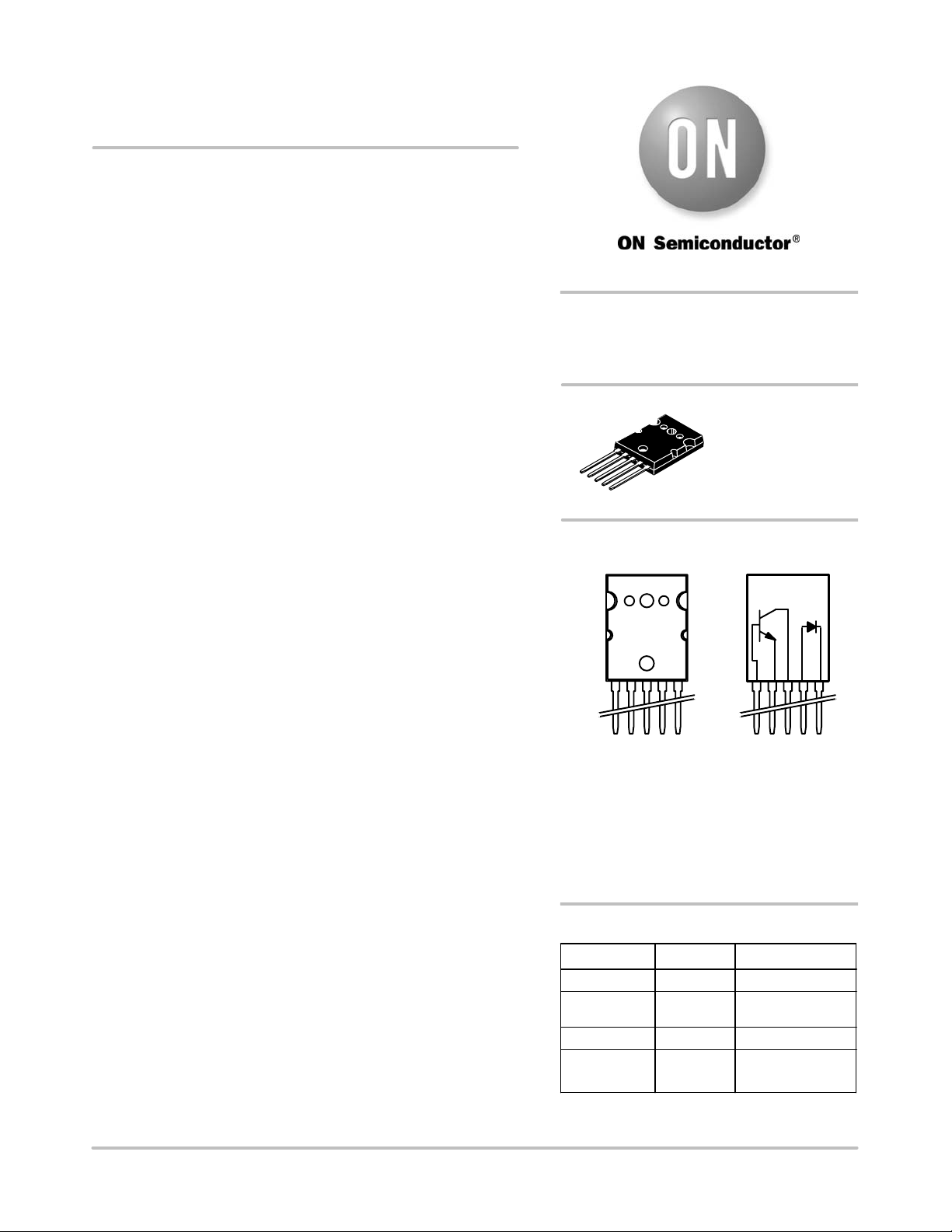
NJL4281D (NPN)
NJL4302D (PNP)
Complementary
ThermalTrakt Transistors
The ThermalTrak family of devices has been designed to eliminate
thermal equilibrium lag time and bias trimming in audio amplifier
applications. They can also be used in other applications as transistor
die protection devices.
Features
• Thermally Matched Bias Diode
• Instant Thermal Bias Tracking
• Absolute Thermal Integrity
• High Safe Operating Area
• Pb−Free Packages are Available*
Benefits
• Eliminates Thermal Equilibrium Lag Time and Bias Trimming
• Superior Sound Quality Through Improved Dynamic Temperature
Response
• Significantly Improved Bias Stability
• Simplified Assembly
♦ Reduced Labor Costs
♦ Reduced Component Count
• High Reliability
http://onsemi.com
BIPOLAR POWER
TRANSISTORS
15 AMP, 350 VOLT, 230 WATT
TO−264, 5 LEAD
CASE 340AA
STYLE 1
MARKING DIAGRAM
NJLxxxxDG
AYYWW
Thermal Trak
SCHEMATIC
Applications
• High−End Consumer Audio Products
♦ Home Amplifiers
♦ Home Receivers
• Professional Audio Amplifiers
♦ Theater and Stadium Sound Systems
♦ Public Address Systems (PAs)
*For additional information on our Pb−Free strategy and soldering details, please
download the ON Semiconductor Soldering and Mounting Techniques
Reference Manual, SOLDERRM/D.
NJLxxxxD =Device Code
G = Pb−Free Package
A =Assembly Location
YY =Year
WW =Work Week
ORDERING INFORMATION
Device Package Shipping
NJL4281D TO−264 25 Units / Rail
NJL4281DG
NJL4302D
NJL4302DG
xxxx = 4281 or 4302
TO−264
(Pb−Free)
TO−264
TO−264
(Pb−Free)
25 Units / Rail
25 Units / Rail
25 Units / Rail
© Semiconductor Components Industries, LLC, 2006
June, 2006 − Rev. 2
1 Publication Order Number:
NJL4281D/D
NJL4281D (NPN) NJL4302D (PNP)
MAXIMUM RATINGS (T
= 25°C unless otherwise noted)
J
Rating Symbol Value Unit
Collector−Emitter Voltage V
Collector−Base Voltage V
Emitter−Base Voltage V
Collector−Emitter Voltage − 1.5 V V
CEO
CBO
EBO
CEX
Collector Current − Continuous
− Peak (Note 1)
Base Current − Continuous I
Total Power Dissipation @ TC = 25°C
P
Derate Above 25°C
Operating and Storage Junction Temperature Range TJ, T
DC Blocking Voltage V
Average Rectified Forward Current I
F(AV)
I
C
B
D
stg
R
350 Vdc
350 Vdc
5 Vdc
350 Vdc
15
30
1.5 Adc
230
1.84
− 65 to +150
200 V
1.0 A
Adc
W
W/°C
°C
THERMAL CHARACTERISTICS
Characteristic Symbol Max Unit
Thermal Resistance, Junction−to−Case
R
q
JC
0.54 °C/W
Stresses exceeding Maximum Ratings may damage the device. Maximum Ratings are stress ratings only. Functional operation above the
Recommended Operating Conditions is not implied. Extended exposure to stresses above the Recommended Operating Conditions may affect
device reliability.
1. Pulse Test: Pulse Width = 5 ms, Duty Cycle < 10%.
ATTRIBUTES
Characteristic Value
ESD Protection Human Body Model
Machine Model
Flammability Rating UL 94 V−0 @ 0.125 in
>8000 V
> 400 V
http://onsemi.com
2
NJL4281D (NPN) NJL4302D (PNP)
ELECTRICAL CHARACTERISTICS (T
= 25°C unless otherwise noted)
C
Characteristic Symbol Min Max Unit
OFF CHARACTERISTICS
Collector Emitter Sustaining Voltage
(IC = 50 mA, IB = 0)
Collector Cut−off Current
(VCE = 200 V, IB = 0)
Collector Cutoff Current
(VCB = 350 Vdc, IE = 0)
Emitter Cutoff Current
(VEB = 5.0 Vdc, IC = 0)
SECOND BREAKDOWN
Second Breakdown Collector with Base Forward Biased
(VCE = 50 Vdc, t = 1.0 s (non−repetitive)
(VCE = 100 Vdc, t = 1.0 s (non−repetitive)
ON CHARACTERISTICS
DC Current Gain
(IC = 100 mAdc, VCE = 5.0 Vdc)
(IC = 1.0 Adc, VCE = 5.0 Vdc)
(IC = 3.0 Adc, VCE = 5.0 Vdc)
(IC = 5.0 Adc, VCE = 5.0 Vdc)
(IC = 8.0 Adc, VCE = 5.0 Vdc)
(IC = 15 Adc, VCE = 5.0 Vdc)
Collector−Emitter Saturation Voltage
(IC = 8.0 Adc, IB = 0.8 Adc)
Emitter−Base Saturation Voltage
(IC = 8.0 Adc, IB = 0.8 A)
Base−Emitter ON Voltage
(IC = 8.0 Adc, VCE = 5.0 Vdc)
DYNAMIC CHARACTERISTICS
Current−Gain − Bandwidth Product
(IC = 1.0 Adc, VCE = 5.0 Vdc, f
= 1.0 MHz)
test
Output Capacitance
(VCB = 10 Vdc, IE = 0, f
= 1.0 MHz)
test
Maximum Instantaneous Forward Voltage (Note 2)
(iF = 1.0 A, TJ = 25°C)
(iF = 1.0 A, TJ = 150°C)
Maximum Instantaneous Reverse Current (Note 2)
(Rated dc Voltage, TJ = 25°C)
(Rated dc Voltage, TJ = 150°C)
Maximum Reverse Recovery Time
(iF = 1.0 A, di/dt = 50 A/ms)
2. Diode Pulse Test: Pulse Width = 300 ms, Duty Cycle v 2.0%.
V
CE(sus)
I
CEO
I
CBO
I
EBO
I
S/b
h
V
CE(sat)
V
BE(sat)
V
BE(on)
C
v
350 − Vdc
− 100
mAdc
mAdc
− 50
mAdc
− 5.0
Adc
FE
4.5
1.0
80
80
80
80
40
10
−
−
−
250
250
250
250
−
−
Vdc
− 1.0
Vdc
− 1.4
Vdc
− 1.5
f
T
ob
F
35 −
− 600
1.1
MHz
pF
V
0.93
i
R
10
mA
100
t
rr
100 ns
http://onsemi.com
3
 Loading...