

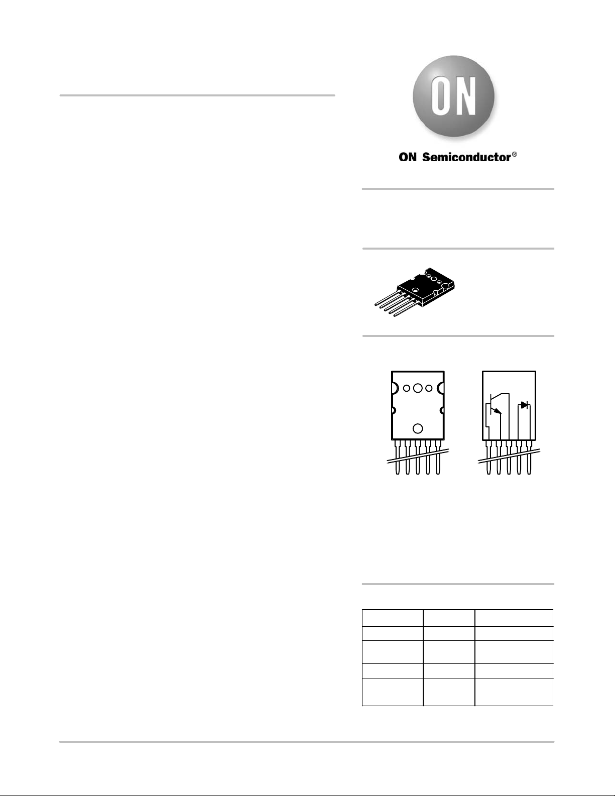
NJL4281D (NPN)
NJL4302D (PNP)
Complementary
ThermalTrakt Transistors
The ThermalTrak family of devices has been designed to eliminate
thermal equilibrium lag time and bias trimming in audio amplifier
applications. They can also be used in other applications as transistor
die protection devices.
Features
• Thermally Matched Bias Diode
• Instant Thermal Bias Tracking
• Absolute Thermal Integrity
• High Safe Operating Area
• Pb−Free Packages are Available*
Benefits
• Eliminates Thermal Equilibrium Lag Time and Bias Trimming
• Superior Sound Quality Through Improved Dynamic Temperature
Response
• Significantly Improved Bias Stability
• Simplified Assembly
♦ Reduced Labor Costs
♦ Reduced Component Count
• High Reliability
http://onsemi.com
BIPOLAR POWER
TRANSISTORS
15 AMP, 350 VOLT, 230 WATT
TO−264, 5 LEAD
CASE 340AA
STYLE 1
MARKING DIAGRAM
NJLxxxxDG
AYYWW
Thermal Trak
SCHEMATIC
Applications
• High−End Consumer Audio Products
♦ Home Amplifiers
♦ Home Receivers
• Professional Audio Amplifiers
♦ Theater and Stadium Sound Systems
♦ Public Address Systems (PAs)
*For additional information on our Pb−Free strategy and soldering details, please
download the ON Semiconductor Soldering and Mounting Techniques
Reference Manual, SOLDERRM/D.
NJLxxxxD =Device Code
G = Pb−Free Package
A =Assembly Location
YY =Year
WW =Work Week
ORDERING INFORMATION
Device Package Shipping
NJL4281D TO−264 25 Units / Rail
NJL4281DG
NJL4302D
NJL4302DG
xxxx = 4281 or 4302
TO−264
(Pb−Free)
TO−264
TO−264
(Pb−Free)
25 Units / Rail
25 Units / Rail
25 Units / Rail
© Semiconductor Components Industries, LLC, 2006
June, 2006 − Rev. 2
1 Publication Order Number:
NJL4281D/D
NJL4281D (NPN) NJL4302D (PNP)
MAXIMUM RATINGS (T
= 25°C unless otherwise noted)
J
Rating Symbol Value Unit
Collector−Emitter Voltage V
Collector−Base Voltage V
Emitter−Base Voltage V
Collector−Emitter Voltage − 1.5 V V
CEO
CBO
EBO
CEX
Collector Current − Continuous
− Peak (Note 1)
Base Current − Continuous I
Total Power Dissipation @ TC = 25°C
P
Derate Above 25°C
Operating and Storage Junction Temperature Range TJ, T
DC Blocking Voltage V
Average Rectified Forward Current I
F(AV)
I
C
B
D
stg
R
350 Vdc
350 Vdc
5 Vdc
350 Vdc
15
30
1.5 Adc
230
1.84
− 65 to +150
200 V
1.0 A
Adc
W
W/°C
°C
THERMAL CHARACTERISTICS
Characteristic Symbol Max Unit
Thermal Resistance, Junction−to−Case
R
q
JC
0.54 °C/W
Stresses exceeding Maximum Ratings may damage the device. Maximum Ratings are stress ratings only. Functional operation above the
Recommended Operating Conditions is not implied. Extended exposure to stresses above the Recommended Operating Conditions may affect
device reliability.
1. Pulse Test: Pulse Width = 5 ms, Duty Cycle < 10%.
ATTRIBUTES
Characteristic Value
ESD Protection Human Body Model
Machine Model
Flammability Rating UL 94 V−0 @ 0.125 in
>8000 V
> 400 V
http://onsemi.com
2
NJL4281D (NPN) NJL4302D (PNP)
ELECTRICAL CHARACTERISTICS (T
= 25°C unless otherwise noted)
C
Characteristic Symbol Min Max Unit
OFF CHARACTERISTICS
Collector Emitter Sustaining Voltage
(IC = 50 mA, IB = 0)
Collector Cut−off Current
(VCE = 200 V, IB = 0)
Collector Cutoff Current
(VCB = 350 Vdc, IE = 0)
Emitter Cutoff Current
(VEB = 5.0 Vdc, IC = 0)
SECOND BREAKDOWN
Second Breakdown Collector with Base Forward Biased
(VCE = 50 Vdc, t = 1.0 s (non−repetitive)
(VCE = 100 Vdc, t = 1.0 s (non−repetitive)
ON CHARACTERISTICS
DC Current Gain
(IC = 100 mAdc, VCE = 5.0 Vdc)
(IC = 1.0 Adc, VCE = 5.0 Vdc)
(IC = 3.0 Adc, VCE = 5.0 Vdc)
(IC = 5.0 Adc, VCE = 5.0 Vdc)
(IC = 8.0 Adc, VCE = 5.0 Vdc)
(IC = 15 Adc, VCE = 5.0 Vdc)
Collector−Emitter Saturation Voltage
(IC = 8.0 Adc, IB = 0.8 Adc)
Emitter−Base Saturation Voltage
(IC = 8.0 Adc, IB = 0.8 A)
Base−Emitter ON Voltage
(IC = 8.0 Adc, VCE = 5.0 Vdc)
DYNAMIC CHARACTERISTICS
Current−Gain − Bandwidth Product
(IC = 1.0 Adc, VCE = 5.0 Vdc, f
= 1.0 MHz)
test
Output Capacitance
(VCB = 10 Vdc, IE = 0, f
= 1.0 MHz)
test
Maximum Instantaneous Forward Voltage (Note 2)
(iF = 1.0 A, TJ = 25°C)
(iF = 1.0 A, TJ = 150°C)
Maximum Instantaneous Reverse Current (Note 2)
(Rated dc Voltage, TJ = 25°C)
(Rated dc Voltage, TJ = 150°C)
Maximum Reverse Recovery Time
(iF = 1.0 A, di/dt = 50 A/ms)
2. Diode Pulse Test: Pulse Width = 300 ms, Duty Cycle v 2.0%.
V
CE(sus)
I
CEO
I
CBO
I
EBO
I
S/b
h
V
CE(sat)
V
BE(sat)
V
BE(on)
C
v
350 − Vdc
− 100
mAdc
mAdc
− 50
mAdc
− 5.0
Adc
FE
4.5
1.0
80
80
80
80
40
10
−
−
−
250
250
250
250
−
−
Vdc
− 1.0
Vdc
− 1.4
Vdc
− 1.5
f
T
ob
F
35 −
− 600
1.1
MHz
pF
V
0.93
i
R
10
mA
100
t
rr
100 ns
http://onsemi.com
3

NJL4281D (NPN) NJL4302D (PNP)
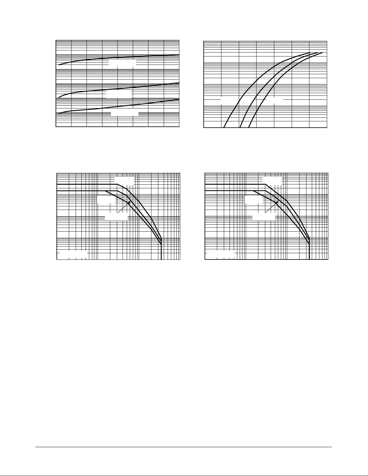
TYPICAL CHARACTERISTICS
1000
TJ = 100°C
100
hFE, DC CURRENT GAIN
10
0.01 0.1 1 10 100
TJ = 25°C
IC, COLLECTOR CURRENT (A)
Figure 1. DC Current Gain, VCE = 5 V,
NPN NJL4281D
1000
TJ = 100°C
100
TJ = 25°C
1000
TJ = 100°C
100
hFE, DC CURRENT GAIN
10
0.01 0.1 1 10 100
TJ = 25°C
IC, COLLECTOR CURRENT (A)
Figure 2. DC Current Gain, VCE = 5 V,
PNP NJL4302D
1000
TJ = 100°C
100
TJ = 25°C
hFE, DC CURRENT GAIN
10
0.01 0.1 1 10 100
IC, COLLECTOR CURRENT (A)
Figure 3. DC Current Gain, VCE = 20 V,
NPN NJL4281D
1.4
1.2
1
0.8
0.6
0.4
SATURATION VOLTAGE (V)
0.2
0
0.01 0.1 1 10 100
V
be(sat)
V
ce(sat)
IC, COLLECTOR CURRENT (A)
TJ = 25°C
Ic/Ib = 10
Figure 5. Typical Saturation Voltage,
NPN NJL4281D
hFE, DC CURRENT GAIN
10
0.01 0.1 1 10 100
IC, COLLECTOR CURRENT (A)
Figure 4. DC Current Gain, VCE = 20 V,
PNP NJL4302D
2.0
1.8
1.6
1.4
1.2
1.0
V
0.8
0.6
0.4
SATURATION VOLTAGE (V)
0.2
0.0
0.01 0.1 1 10 100
IC, COLLECTOR CURRENT (A)
be(sat)
V
ce(sat)
Figure 6. Typical Saturation Voltage,
PNP NJL4302D
TJ = 25°C
Ic/Ib = 10
http://onsemi.com
4

NJL4281D (NPN) NJL4302D (PNP)
V
, BASE−EMITTER VOLTAGE
0
fT, CURRENT BANDWIDTH PRODUCT (MHz)
0
,
TYPICAL CHARACTERISTICS
1.4
1.2
1.0
0.8
(V)
0.6
0.4
0.2
BE(on)
0.0
0.01 0.1 1 10 100
IC, COLLECTOR CURRENT (A)
Figure 7. Typical Base−Emitter Voltages,
NPN NJL4281D
70
60
50
40
30
V
= 5 V
CE
V
= 10 V
CE
2.5
2.0
1.5
(V)
1.0
, BASE−EMITTER VOLTAGE
0.5
BE(on)
V
0.0
0.01 0.1 1 10 10
IC, COLLECTOR CURRENT (A)
Figure 8. Typical Base−Emitter Voltages,
PNP NJL4302D
70
60
50
40
30
V
= 5 V
CE
V
= 10 V
CE
20
10
TJ = 25°C
f
= 1 MHz
test
0
0.1 1 10
IC, COLLECTOR CURRENT (A)
Figure 9. Typical Current Gain Bandwidth Product,
NPN NJL4281D
20
10
TJ = 25°C
f
= 1 MHz
test
0
fT, CURRENT BANDWIDTH PRODUCT (MHz)
0.1 1 1
Figure 10. Typical Current Gain Bandwidth Product
PNP NJL4302D
http://onsemi.com
5
NJL4281D (NPN) NJL4302D (PNP)
1E−05
1E−06
1E−07
1E−08
1E−09
, REVERSE CURRENT (mA)
R
1E−10
I
1E−11
100
TJ = 100°C
TJ = 25°C
TJ = −25°C
0
VR, REVERSE VOLTAGE (VOLTS)
20015010050 400
250 300
Figure 11. Typical Diode Reverse Current
10 mS
10
1 Sec
350
10
1
0.1
0.01
, FORWARD CURRENT (A)
F
I
0.001
0.1
100°C
Figure 12. Typical Diode Forward Voltage
100
10
25°C
VF, VOLTAGE (VOLTS)
1 Sec
−25°C
0.70.50.3 0.9
10 mS
1.31.1
1.5
1
0.1
, COLLECTOR CURRENT (A)
C
I
TJ = 25°C
0.01
1 10 100 1000
Vce, COLLECTOR−EMITTER VOLTAGE (V)
100 mS
Figure 13. Active Region Safe Operating Area,
NPN NJL4281D
1
0.1
, COLLECTOR CURRENT (A)
C
I
TJ = 25°C
0.01
1 10 100 1000
Vce, COLLECTOR−EMITTER VOLTAGE (V)
100 mS
Figure 14. Active Region Safe Operating Area,
PNP NJL4302D
http://onsemi.com
6
NJL4281D (NPN) NJL4302D (PNP)
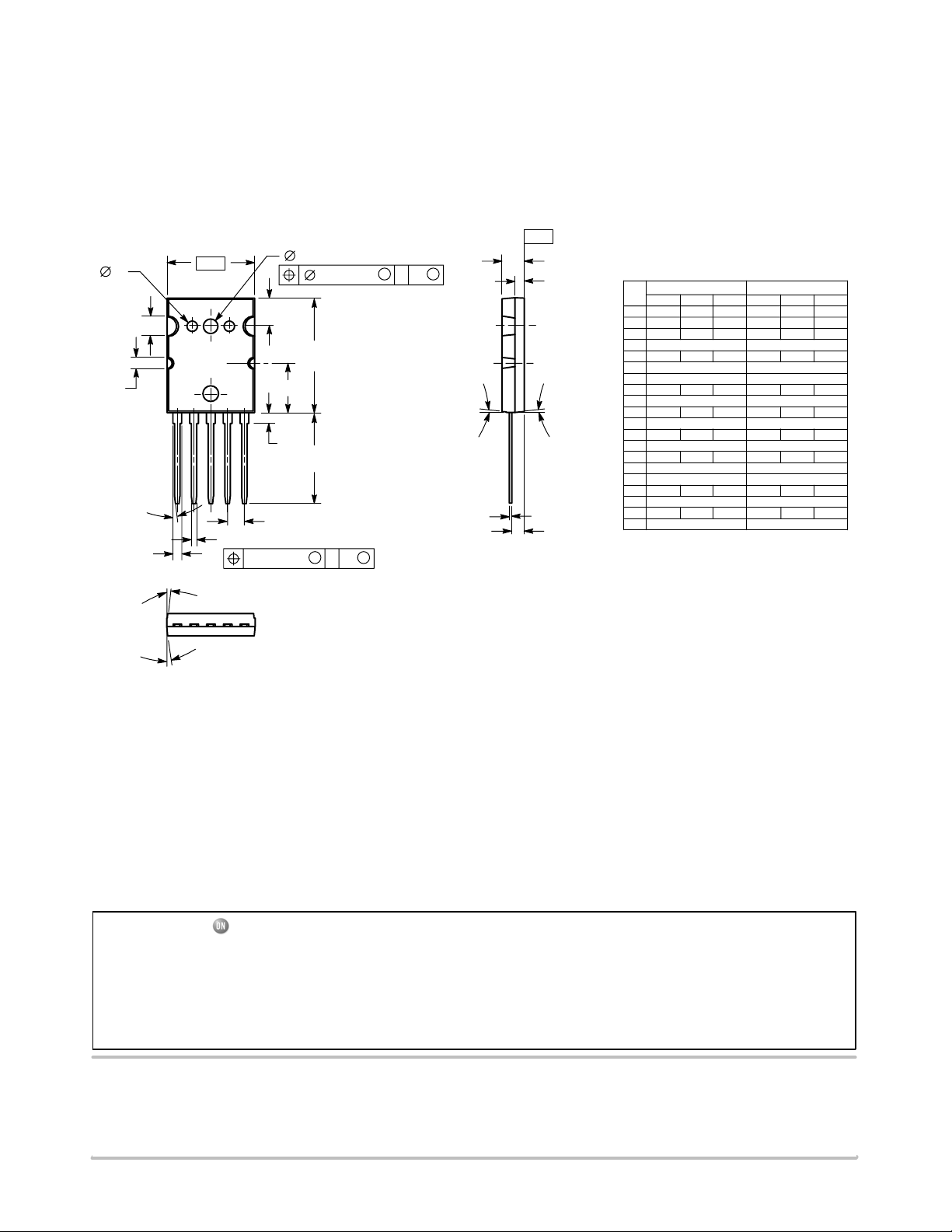
PACKAGE DIMENSIONS
TO−264, 5 LEAD
CASE 340AA−01
ISSUE O
−T−
Y
−B−
Q
0.25 (0.010) MTB
M
C
E
U
N
A
R
12 3
45
L
SW
P
K
M
F
5 PL
G
D
5 PL
0.25 (0.010) MTB
S
J
H
W
NOTES:
1. DIMENSIONING AND TOLERANCING PER
ANSI Y14.5M, 1982.
2. CONTROLLING DIMENSION: MILLIMETER.
MILLIMETERS
DIM MIN NOM MAX
A 25.857 25.984 26.111
B 19.761 19.888 20.015
C 4.928 5.055 5.182
D 1.219 BSC
E 2.032 2.108 2.184
1.981 BSC
F
G 3.81 BSC
H 2.667 2.718 2.769
J 0.584 BSC
K 20.422 20.549 20.676
L 11.28 REF
0 −−−
M
_
N 4.57 REF
P 2.259 2.386 2.513
Q 3.480 BSC
R 2.54 REF
S
0 −−−
U 6.17 REF
W
0 −−−
Y 2.388 BSC
STYLE 1:
PIN 1. BASE
2. EMITTER
3. COLLECTOR
4. ANODE
5. CATHODE
8 _0
_
6 _0
_
7 _0
INCHES
MIN NOM MAX
1.018 1.023 1.028
0.778 0.783 0.788
0.194 0.199 0.204
0.0480 BSC
0.0800 0.0830 0.0860
0.0780 BSC
0.150 BSC
0.1050 0.1070 0.1090
0.0230 BSC
0.804 0.809
0.444 REF
_
0.180 REF
0.0889 0.0939 0.0989
0.1370 BSC
0.100 REF
_
0.243 REF
_
0.0940 BSC
−−−
−−−
−−−
0.814
7
8
6
_
_
_
S
ThermalTrak is a trademark of Semiconductor Components Industries, LLC (SCILLC).
ON Semiconductor and are registered trademarks of Semiconductor Components Industries, LLC (SCILLC). SCILLC reserves the right to make changes without further notice
to any products herein. SCILLC makes no warranty, representation or guarantee regarding the suitability of its products for any particular purpose, nor does SCILLC assume any liability
arising out of the application or use of any product or circuit, and specifically disclaims any and all liability, including without limitation special, consequential or incidental damages.
“Typical” parameters which may be provided in SCILLC data sheets and/or specifications can and do vary in different applications and actual performance may vary over time. All
operating parameters, including “Typicals” must be validated for each customer application by customer’s technical experts. SCILLC does not convey any license under its patent rights
nor the rights of others. SCILLC products are not designed, intended, or authorized for use as components in systems intended for surgical implant into the body, or other applications
intended to support or sustain life, or for any other application in which the failure of the SCILLC product could create a situation where personal injury or death may occur. Should
Buyer purchase or use SCILLC products for any such unintended or unauthorized application, Buyer shall indemnify and hold SCILLC and its officers, employees, subsidiaries, affiliates,
and distributors harmless against all claims, costs, damages, and expenses, and reasonable attorney fees arising out of, directly or indirectly, any claim of personal injury or death
associated with such unintended or unauthorized use, even if such claim alleges that SCILLC was negligent regarding the design or manufacture of the part. SCILLC is an Equal
Opportunity/Affirmative Action Employer. This literature is subject to all applicable copyright laws and is not for resale in any manner.
PUBLICATION ORDERING INFORMATION
LITERATURE FULFILLMENT:
Literature Distribution Center for ON Semiconductor
P.O. Box 5163, Denver, Colorado 80217 USA
Phone: 303−675−2175 or 800−344−3860 Toll Free USA/Canada
Fax: 303−675−2176 or 800−344−3867 Toll Free USA/Canada
Email: orderlit@onsemi.com
N. American Technical Support: 800−282−9855 Toll Free
USA/Canada
Europe, Middle East and Africa Technical Support:
Phone: 421 33 790 2910
Japan Customer Focus Center
Phone: 81−3−5773−3850
http://onsemi.com
ON Semiconductor Website: www.onsemi.com
Order Literature: http://www.onsemi.com/orderlit
For additional information, please contact your local
Sales Representative
NJL4281D/D
7
 Loading...