

Page 1
9 to 24 Volt Electronic Fuse
NIS4461 Series
The NIS4461 eFuse is a cost effective, resettable fuse which can
greatly enhance the reliability of a hard drive or other circuit from both
catastrophic and shutdown failures.
It is designed to protect the downstream circuitry against an
overcurrent event by limiting the current while protecting against high
inrush current, as well as monitoring the load current in real time.
Features
• Integrated Power Device
• Power Device Thermally Protected
• No External Current Shunt Required
• 9 V to 24 V Input Range
• 39 mW Typical
• Internal Charge Pump
• Internal Undervoltage Lockout Circuit
• ESD Ratings:
Human Body Model (HBM); 2000 V
Charged Device Model (CDM); 2000 V
Latch−Up; Class 1
• These Devices are Pb−Free, Halogen Free/BFR Free and are RoHS
Compliant
Typical Applications
• Hard Drives
• Mother Board Power Management
• Fan Drives
• Industrial
• Handheld Devices
• Portable Instruments
www.onsemi.com
4.2 AMP, 9 to 24 VOLT
ELECTRONIC FUSE
MARKING
DIAGRAM
WDFN10
CASE 522AA
XXX = Specific Device Code
A = Assembly Location
L = Wafer Lot
Y = Year
W = Work Week
G = Pb−Free Package
(Note: Microdot may be in either location)
PIN CONNECTIONS
GND
dV/dt
NC/I
En/Flt
I
LIM
SENSE
V
CC
XXXXX
XXXXX
ALYWG
Src
Src
Src
Src
Src
G
© Semiconductor Components Industries, LLC, 2020
March, 2021 − Rev. 2
WDFN10
(Top View)
See detailed ordering, marking and shipping information in the
ordering information section on page 11 of this data sheet.
1 Publication Order Number:
ORDERING INFORMATION
NIS4461/D
Page 2
NIS4461 Series
VCC
ENABLE/
FAULT
ENABLE/
FAULT
Enable
Thermal
Shutdown
UVLO
Enable
Charge
Pump
Current
Limit
dv/dt
Control
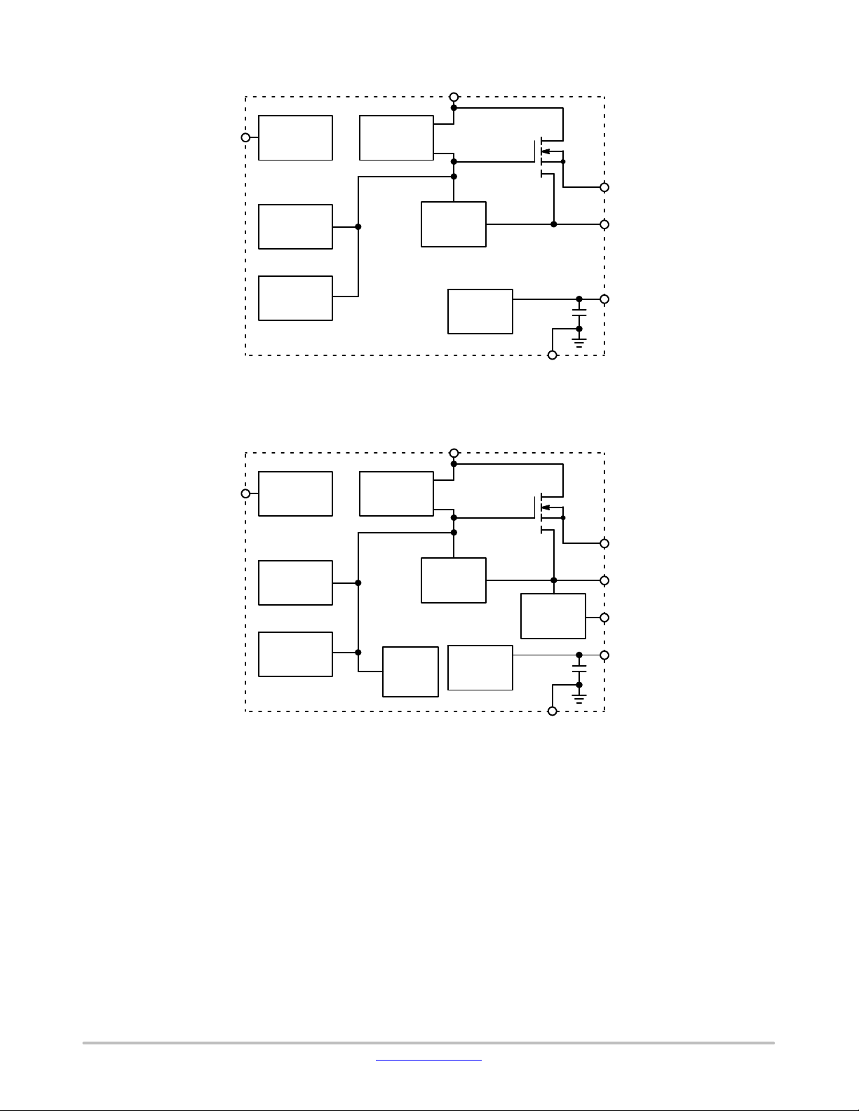
Figure 1. Block Diagram
(NIS4461MT2TXG, NIS4461MT4TXG)
VCC
Charge
Pump
GND
SOURCE
I
LIMIT
dv/dt
Thermal
Shutdown
UVLO
Current
Limit
Voltage
Clamp
dv/dt
Control
Figure 2. Block Diagram
(NIS4461MT1TXG, NIS4461MT3TXG
Current
Monitor
GND
SOURCE
I
LIMIT
I
SENSE
dv/dt
www.onsemi.com
2
Page 3
NIS4461 Series
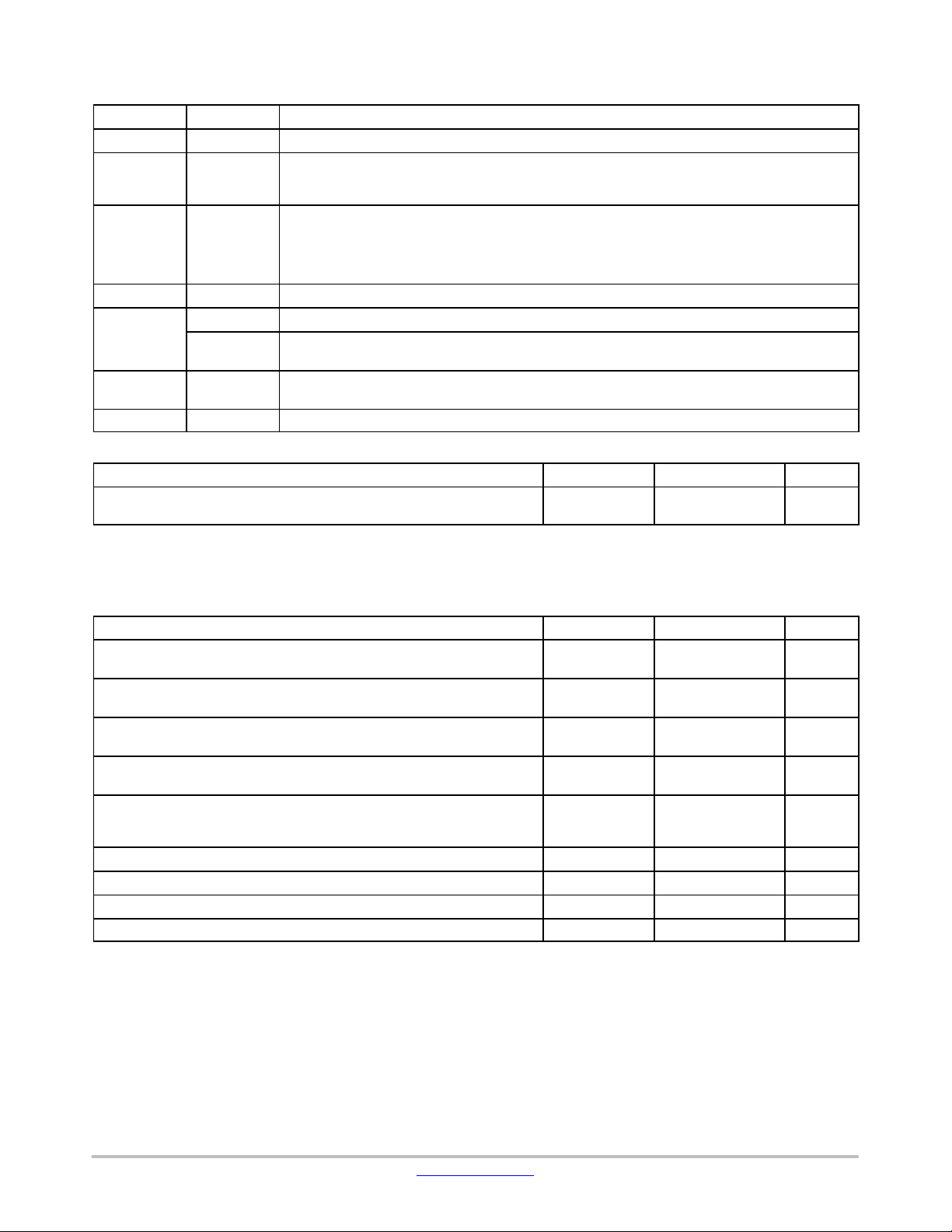
Table 1. FUNCTIONAL PIN DESCRIPTION
Pin Function Description
1 Ground Negative input voltage to the device. This is used as the internal reference for the IC.
2 dv/dt The internal dv/dt circuit controls the slew rate of the output voltage at turn on. It has an internal
3 Enable/Fault The enable/fault pin is a tri−state, bidirectional interface. It can be pulled to ground with external
4 I
5
Limit
NC For NIS4461MT2TXG and NIS4461MT4TXG
I
SENSE
6−10 Source This pin is the source of the internal power FET and the output terminal of the fuse. Connect an
11 (belly pad) V
CC
MAXIMUM RATINGS
Input Voltage, operating, steady−state (VCC to GND, Note 1)
Stresses exceeding those listed in the Maximum Ratings table may damage the device. If any of these limits are exceeded, device functionality
should not be assumed, damage may occur and reliability may be affected.
1. Negative voltage will not damage device provided that the power dissipation is limited to the rated allowable power for the package.
Transient (100 ms)
capacitor that allows it to ramp up over a period of 2 ms. An external capacitor can be added to this
pin to increase the ramp time. If an additional time delay is not required, this pin should be left open.
open−drain or open collector device to shutdown the eFuse. It can also be used as a status indicator;
if the voltage level is intermediate around 1.4 V − the eFuse is in the thermal shutdown, if the voltage
level is high around 3 V − the eFuse is operating normally. Do not actively drive this pin to any
voltage. Do not connect a capacitor to this pin.
A resistor between this pin and the source pin sets the overload and short circuit current limit levels.
For NIS4461MT1TXG and NIS4461MT3TXG load current monitor allows the system to monitor the
load current in real time. Connect R
SENSE
to GND.
electrolytic capacitor or Schottky diode for 27 V or higher.
Positive input voltage to the device.
Rating Symbol Value Unit
V
IN
−0.6 to 30
−0.6 to 30
V
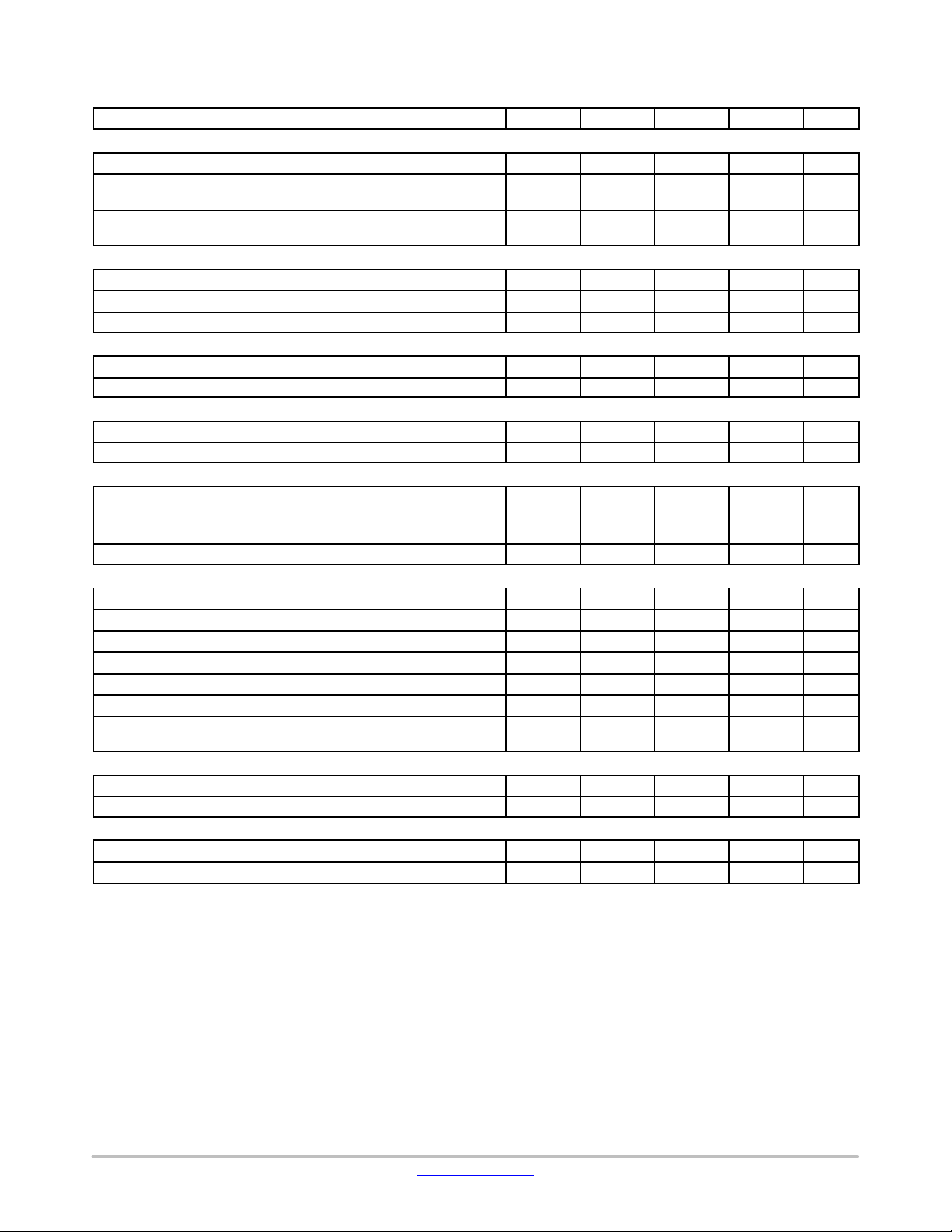
Table 2. THERMAL RATINGS
Rating Symbol Value Unit
Thermal Resistance, Junction−to−Air
(4 layer High−K JEDEC JESD51−7 PCB, 100 mm
Thermal Characterization Parameter, Junction−to−Lead
(4 layer High−K JEDEC JESD51−7 PCB, 100 mm
Thermal Characterization Parameter, Junction−to−Board
(4 layer High−K JEDEC JESD51−7 PCB, 100 mm
Thermal Characterization Parameter, Junction−to−Case Top
(4 layer High−K JEDEC JESD51−7 PCB, 100 mm
Total Power Dissipation @ TA = 25°C
(4 layer High−K JEDEC JESD51−7 PCB, 100 mm
Derate above 25°C
Operating Ambient Temperature Range T
Operating Junction Temperature Range T
Non−operating Temperature Range T
Lead Temperature, Soldering (10 Sec) T
2
, 2 oz. Cu)
2
, 2 oz. Cu)
2
, 2 oz. Cu)
2
, 2 oz. Cu)
2
, 2 oz. Cu)
Y
Y
Y
P
q
max
STG
JA
J−L
J−B
J−T
A
J
L
90 °C/W
27.5 °C/W
27.5 °C/W
7.6 °C/W
1.39
11.1
W
mW/°C
−40 to 125 °C
−40 to 150 °C
−55 to 155 °C
260 °C
www.onsemi.com
3
Page 4
NIS4461 Series
ELECTRICAL CHARACTERISTICS (V
Characteristics
= 24 V, CL = 100 mF, dv/dt pin open, R
CC
Symbol Min Typ Max Unit
= 20 W, Tj = 25°C unless otherwise noted.)
LIMIT
POWER FET
Delay Time (enabling of chip to ID = 100 mA with 1 A resistive load) T
Kelvin ON Resistance (Note 2)
T
= 140°C (Note 3)
J
R
Continuous Current (TA = 25°C, 0.5 in2 copper) (Note 3)
(T
= 80°C, minimum copper)
A
dly
DSon
I
D
I
D
− 220 −
30
−
−
−
39
60
4.2
2.5
50
ms
mW
−
−
A
−
THERMAL LATCH
Shutdown Temperature (Note 3) T
Thermal Hysteresis (Auto−retry part only) T
Thermal Shutdown Response Time T
Hyst
SD
SD
Res
150 175 200 °C
− 45 − °C
10 15 20
ms
UNDERVOLTAGE PROTECTION
Undervoltage Lockout V
UVLO Hysteresis V
UVLO
Hyst
6 6.5 7 V
− 0.80 − V
CURRENT LIMIT
Kelvin Short Circuit Current Limit (R
Kelvin Overload Current Limit (R
Limit
= 20 W, Note 4)
Limit
= 20 W, Note 4)
I
Lim−SS
I
Lim−OL
1.76 2.1 2.64 A
− 4.6 − A
dv/dt CIRCUIT
Output Voltage Ramp Time (Enable to V
Output Voltage Ramp Time
(10% to 90% − V
= 2.4 V to 21.6 V with 24W Load)
OUT
Maximum Capacitor Voltage V
= 23.7 V) t
OUT
slew
t
slew
max
− 2.0 − ms
− 1.2 − ms
− − V
CC
V
ENABLE/FAULT
Logic Level Low (Output Disabled)
Logic Level Mid (Thermal Fault, Output Disabled) V
Logic Level High (Output Enabled) V
High State Maximum Voltage V
Logic Low Sink Current (V
Logic High Leakage Current for External Switch (V
= 0 V) I
enable
= 3.3 V) I
enable
Maximum Fanout for Fault Signal (Total number of chips that can be
V
in−low
in−mid
in−high
in−max
in−low
in−leak
0.35 0.58 0.81 V
0.82 1.4 1.95 V
1.96 2.6 3.0 V
2.51 4.6 5 V
− −15 −25
− − 1.0
Fan − − 3.0 Units
mA
mA
connected to this pin for simultaneous shutdown)
TOTAL DEVICE
Bias Current (Operational)
Bias Current (Shutdown) I
I
Bias
Bias
− − 450
− − 220
mA
mA
LOAD CURRENT MONITOR
Current Monitor Sense (R
SENSE
= 1 kW)
Current Monitor Sense Accuracy I
I
SENSE
ACC
− 1 − mA/A
−10 − 10 %
Product parametric performance is indicated in the Electrical Characteristics for the listed test conditions, unless otherwise noted. Product
performance may not be indicated by the Electrical Characteristics if operated under different conditions.
2. Pulse test: Pulse width 300 ms, duty cycle 2%.
3. Verified by design.
4. Refer to explanation of short circuit and overload conditions in application note AND9441.
5. Device will shut down prior to reaching this level based on actual UVLO trip point.
6. For output slew rate calculation with external capacitor, please refer to ”Output Slew Rate (dv/dt)” in the ”Application Information ” section
www.onsemi.com
4
Page 5

100
10
TIME (ms)
NIS4461 Series
−40_C
25_C
85_C
+12 V
ENABLE
GND
1
01020 405060 80
30 70
POWER (W)
Figure 3. Thermal Trip Time vs. Power Dissipation
I
LIMIT
dv/dtGND
10
9
8
7
6
4
11
V
CC
SOURCE
NIS4461MT2/4
3
ENABLE/
FAULT
12
Figure 4. Application Circuit with Direct Current Sensing
R
S
LOAD
+12 V
ENABLE
GND
11
V
CC
SOURCE
10
9
8
7
3
ENABLE
NIS4461MT1/3
I
SENSE
I
LIMIT
dv/dtGND
6
4
R
SENSE
12
Figure 5. Application Circuit with Direct Current Sensing
www.onsemi.com
5
R
S
LOAD
Page 6

NIS4461 Series
LOAD
SOURCE
I
LIMIT
dv/dt
V
CC
V
CC
NIS5420 NIS4461
ENABLE/
FAULT
GND
ENABLE/
FAULT
GND
ENABLE
Figure 6. Common Thermal Shutdown
SOURCE
I
LIMIT
dv/dt
R
S
LOAD
www.onsemi.com
6
Page 7

NIS4461 Series
TYPICAL CHARACTERISTICS
2.0
1.95
1.9
1.85
1.8
(V)
1.75
SENSE
1.7
VI
1.65
1.6
1.55
1.5
−40 −20 0 20 40 60 80 100
TEMPERATURE (°C)
Figure 7. VI
vs. Temperature
SENSE
50
48
46
44
42
(mW)
40
38
DS(ON)
R
36
34
32
30
0 5 10 15 20 25 30
(V)
V
CC
Figure 9. R
DS(ON)
vs. V
CC
4.5
4
3.5
3
(V)
2.5
2
SENSE
VI
1.5
1
0.5
0
0 0.5 1 1.5 2 2.5 3 3.5 4
LOAD CURRENT (A)
Figure 8. VI
vs. Load Current
SENSE
100
90
80
70
60
(mW)
50
40
DS(ON)
R
30
20
10
0
−40 −20 0 20 40 60 100
TEMPERATURE (°C)
Figure 10. R
vs. Temperature
DS(ON)
4.5 5
80
10
9
IOL, R
LIM
= 10 W
8
(A)
SC
/I
OL
I
7
6
5
4
IOL, R
LIM
= 40 W
ISC, R
IOL, R
LIM
LIM
= 10 W
= 20 W
3
2
1
0
ISC, R
LIM
= 40 W
ISC, R
LIM
= 20 W
−40 −20 0 20 40 60 100
TEMPERATURE (°C)
Figure 11. IOL and ISC vs. Temperature
(A)
SC
/I
OL
I
80
www.onsemi.com
7
8
7
6
5
4
I
OL
3
2
I
SC
1
0
010 30 50 70
20 40 60
R
(W)
LIM
Figure 12. IOL and ISC vs. R
LIM
Page 8

NIS4461 Series
TYPICAL CHARACTERISTICS
30
VCC = 24 V
I
LOAD
25
20
(ms)
15
SLEW
T
10
5
= 1 A
Figure 13. Slew Rate Control Screenshot
1.4
1.2
1
0.8
(ms)
0.6
SLEW
T
0.4
0.2
0
−40 0 20 60 100
TEMPERATURE (°C)
Figure 15. T
SLEW
40−20 80
vs. Temperature
0
0 100 600
Figure 14. T
7.0
6.8
6.6
6.4
6.2
6.0
5.8
5.6
UVLO TURN ON (V)
5.4
5.2
5.0
−40 −20 0 20 40 60 100
200 300 400 500
Capacitance from dV/dt Pin to GND (pF)
vs. dV/dt Capacitance
SLEW
TEMPERATURE (°C)
Figure 16. UVLO TURN ON vs. Temperature
80
www.onsemi.com
8
Page 9

NIS4461 Series
APPLICATION INFORMATION
Basic Operation
This device is a self−protected, resettable, electronic fuse.
It contains circuits to monitor the input voltage, output
voltage, output current and die temperature.
On application of the input voltage, the device will apply
the input voltage to the load based on the restrictions of the
controlling circuits. The dv/dt of the output voltage will be
controlled by the internal dv/dt circuit. The output voltage
will slew from 0 V to the rated output voltage in 1 ms, unless
additional capacitance is added to the dv/dt pin.
The device will remain on as long as the temperature does
not exceed the 175°C limit that is programmed into the chip.
The current limit circuit does not shut down the part but will
reduce the conductivity of the FET to maintain a constant
current at the internally set current limit level.
An internal charge pump provides bias for the gate voltage
of the internal n−channel power FET and also for the current
limit circuit. The remainder of the control circuitry operates
between the input voltage (V
Current Limit
) and ground.
CC
The current limit circuit uses a SENSEFET along with a
reference and amplifier to control the peak current in the
device. The SENSEFET allows for a small fraction of the
load current to be measured, which has the advantage of
reducing the losses in the sense resistor as well as increasing
the value and decreasing the power rating of the sense
resistor. Sense resistors are typically in the tens of ohms
range with power ratings of several milliwatts making them
very inexpensive chip resistors.
The current limit circuit has two limiting values, one for
short circuit events which are defined as the mode of
operation in which the gate is high and the FET is fully
enhanced. The overload mode of operation occurs when the
device is actively limiting the current and the gate is at an
intermediate level. For a more detailed description of this
circuit please refer to application note AND9441.
There are two methods of biasing the current limit circuit
for this device. They are shown in the two application
figures. Direct current sensing connects the sense resistor
between the current limit pin and the load. This method
includes the bond wire resistance in the current limit circuit.
This resistance has an impact on the current limit levels for
a given resistor and may vary slightly depending on the
impedance between the sense resistor and the source pins.
The on resistance of the device will be slightly lower in this
configuration since all five source pins are connected in
parallel and therefore, the effective bond wire resistance is
one fifth of the resistance for any given pin.
The other method is Kelvin sensing. This method uses one
of the source pins as the connection for the current sense
resistor. This connection senses the voltage on the die and
therefore any bond wire resistance and external impedance
on the board have no effect on the current limit levels. In this
configuration the on resistance is slightly increased relative
to the direct sense method since only four of the source pins
are used for power.
Undervoltage Lockout
The undervoltage lockout circuit uses a comparator with
hysteresis to monitor the input voltage. If the input voltage
drops below the specified level, the output switch will be
switched to a high impedance state.
Output Slew Rate dv/dt
The dv/dt circuit brings the output voltage up under a
linear, controlled rate regardless of the load impedance
characteristics. An internal ramp generator creates a linear
ramp, and a control circuit forces the output voltage to
follow that ramp, scaled by a factor.
The default ramp time is approximately 1 ms. This can be
modified by adding an external capacitor at the dv/dt pin.
This pin includes an internal current source of
approximately 85 nA. Since the current level is very low, it
is important to use a ceramic cap or other low leakage
capacitor. Aluminum electrolytic capacitors are not
recommended for this circuit.
The ramp time from 0 to the nominal output voltage can
be determined by the following equation, where t is in
seconds:
t
2.4*21.6
C
+ 3.8e7 @ǒ28 pF ) C
ǒ
ext
t
+
2.4−21.6
* 0.00127
3.8e7
Ǔ
) 0.00127
ext
Ǔ
* 28 pF
Where:
C is in Farads
t is in seconds
Any time that the unit shuts down due to a fault, enable
shut−down, or recycling of input power, the timing capacitor
will be discharged and the output voltage will ramp from 0
at turn on.
Enable/Fault
The Enable/Fault pin is a multi−function, bidirectional pin
that can control the output of the chip as well as send
information to other devices regarding the state of the chip.
When this pin is low, the output of the fuse will be turned off.
When this pin is high the output of the fuse will be
turned−on. If a thermal fault occurs, this pin will be pulled
low to an intermediate level by an internal circuit.
To use as a simple enable pin, an open drain or open
collector device should be connected to this pin. Due to its
tri−state operation, it should not be connected to any type of
logic with an internal pullup device.
If the chip shuts down due to the die temperature reaching
its thermal limit, this pin will be pulled down to an
intermediate level. This signal can be monitored by an
external circuit to communicate that a thermal shutdown has
occurred. If this pin is tied to another device in this family,
www.onsemi.com
9
Page 10

NIS4461 Series
a thermal shutdown of one device will cause both devices to
disable their outputs. Both devices will turn on once the fault
is removed for the auto−retry devices.
For the latching thermal device, the outputs will be
enabled after the enable pin has been pulled to ground with
an external switch and then allowed to go high or after the
input power has been recycled. For the auto retry devices,
both devices will restart as soon as the die temperature of the
device in shutdown has been reduced to the lower thermal
limit.
Thermal Protection
The NIS4461 includes an internal temperature sensing
circuit that senses the temperature on the die of the power
3.3 V
1.95 V
FET. If the temperature reaches 175°C, the device will shut
down, and remove power from the load. Output power can
be restored by either recycling the input power or toggling
the enable pin for thermally latching devices. Power will
automatically be reapplied to the load for auto−retry devices
once the die temperature has been reduced by 45°C.
The thermal limit has been set high intentionally, to
increase the trip time during high power transient events. It
is not recommended to operate this device above 150°C for
extended periods of time.
Enable/Fault
0.81 V
Gnd
Figure 17. Fault/Enable Signal Levels
12 mA
1.4 V
SD
Startup
Blanking
Thermal
Shutdown
2.64 V
0.58 V
+
−
−
+
Thermal Reset
Thermal SD
Enable SD
Figure 18. Enable/Fault Simplified Circuit
www.onsemi.com
10
Page 11

NIS4461 Series
ORDERING INFORMATION
Device Marking Features ISENSE Package Shipping
NIS4461MT1TXG 61T1 Thermal Latching Ye s
NIS4461MT2TXG 61T2 Thermal Latching No
NIS4461MT3TXG 61T3 Auto−Retry Ye s
NIS4461MT4TXG 61T4 Auto−Retry No
†For information on tape and reel specifications, including part orientation and tape sizes, please refer to our Tape and Reel Packaging
Specifications Brochure, BRD8011/D.
WDFN10
(Pb−Free)
3000 / Tape & Reel
†
www.onsemi.com
11
Page 12

NIS4461 Series
PACKAGE DIMENSIONS
WDFN10, 3x3, 0.5P
CASE 522AA
ISSUE A
10X
REFERENCE
2X
2X
PIN ONE
0.15 C
0.10 C
0.08 C
10X
0.15 C
L
D
TOP VIEW
SIDE VIEW
D2
1
NOTES:
1. DIMENSIONING AND TOLERANCING PER
ASME Y14.5M, 1994.
2. CONTROLLING DIMENSION: MILLIMETERS.
3. DIMENSION b APPLIES TO PLATED
TERMINAL AND IS MEASURED BETWEEN
0.15 AND 0.30mm FROM TERMINAL.
4. COPLANARITY APPLIES TO THE EXPOSED
PAD AS WELL AS THE TERMINALS.
DIMAMIN NOM MAX
A1 0.00 0.03 0.05
A3 0.20 REF
b 0.18 0.24 0.30
D 3.00 BSC
D2 2.45 2.50 2.55
E 3.00 BSC
E2
e 0.50 BSC
K
L
MILLIMETERS
0.70 0.75 0.80
1.75 1.80 1.85
0.19 TYP
0.35 0.40 0.45
A3
B
A
E
A
A1
SEATING
C
PLANE
SOLDERING FOOTPRINT*
2.6016
e
5
E2
2.1746
1.8508
3.3048
10X
K 10
BOTTOM VIEW
6
b
10X
0.05 C
A0.10 C
B
NOTE 3
10X
0.5651
10X
0.3008
0.5000 PITCH
DIMENSIONS: MILLIMETERS
*For additional information on our Pb−Free strategy and soldering
details, please download the ON Semiconductor Soldering and
Mounting Techniques Reference Manual, SOLDERRM/D.
ON Semiconductor and are trademarks of Semiconductor Components Industries, LLC dba ON Semiconductor or its subsidiaries in the United States and/or other countries.
ON Semiconductor owns the rights to a number of patents, trademarks, copyrights, trade secrets, and other intellectual property. A listing of ON Semiconductor’s product/patent
coverage may be accessed at www.onsemi.com/site/pdf/Patent−Marking.pdf
ON Semiconductor makes no warranty, representation or guarantee regarding the suitability of its products for any particular purpose, nor does ON Semiconductor assume any liability
arising out of the application or use of any product or circuit, and specifically disclaims any and all liability, including without limitation special, consequential or incidental damages.
Buyer is responsible for its products and applications using ON Semiconductor products, including compliance with all laws, regulations and safety requirements or standards,
regardless of any support or applications information provided by ON Semiconductor. “Typical” parameters which may be provided in ON Semiconductor data sheets and/or
specifications can and do vary in different applications and actual performance may vary over time. All operating parameters, including “Typicals” must be validated for each customer
application by customer’s technical experts. ON Semiconductor does not convey any license under its patent rights nor the rights of others. ON Semiconductor products are not
designed, intended, or authorized for use as a critical component in life support systems or any FDA Class 3 medical devices or medical devices with a same or similar classification
in a foreign jurisdiction or any devices intended for implantation in the human body. Should Buyer purchase or use ON Semiconductor products for any such unintended or unauthorized
application, Buyer shall indemnify and hold ON Semiconductor and its officers, employees, subsidiaries, affiliates, and distributors harmless against all claims, costs, damages, and
expenses, and reasonable attorney fees arising out of, directly or indirectly, any claim of personal injury or death associated with such unintended or unauthorized use, even if such
claim alleges that ON Semiconductor was negligent regarding the design or manufacture of the part. ON Semiconductor is an Equal Opportunity/Affirmative Action Employer. This
literature is subject to all applicable copyright laws and is not for resale in any manner.
. ON Semiconductor reserves the right to make changes without further notice to any products herein.
PUBLICATION ORDERING INFORMATION
LITERATURE FULFILLMENT:
Email Requests to: orderlit@onsemi.com
ON Semiconductor Website: www.onsemi.com
TECHNICAL SUPPORT
North American Technical Support:
Voice Mail: 1 800−282−9855 Toll Free USA/Canada
Phone: 011 421 33 790 2910
Europe, Middle East and Africa Technical Support:
Phone: 00421 33 790 2910
For additional information, please contact your local Sales Representative
◊
www.onsemi.com
12
 Loading...