

NIF62514
Preferred Device
Self-Protected FET
with Temperature and
Current Limit
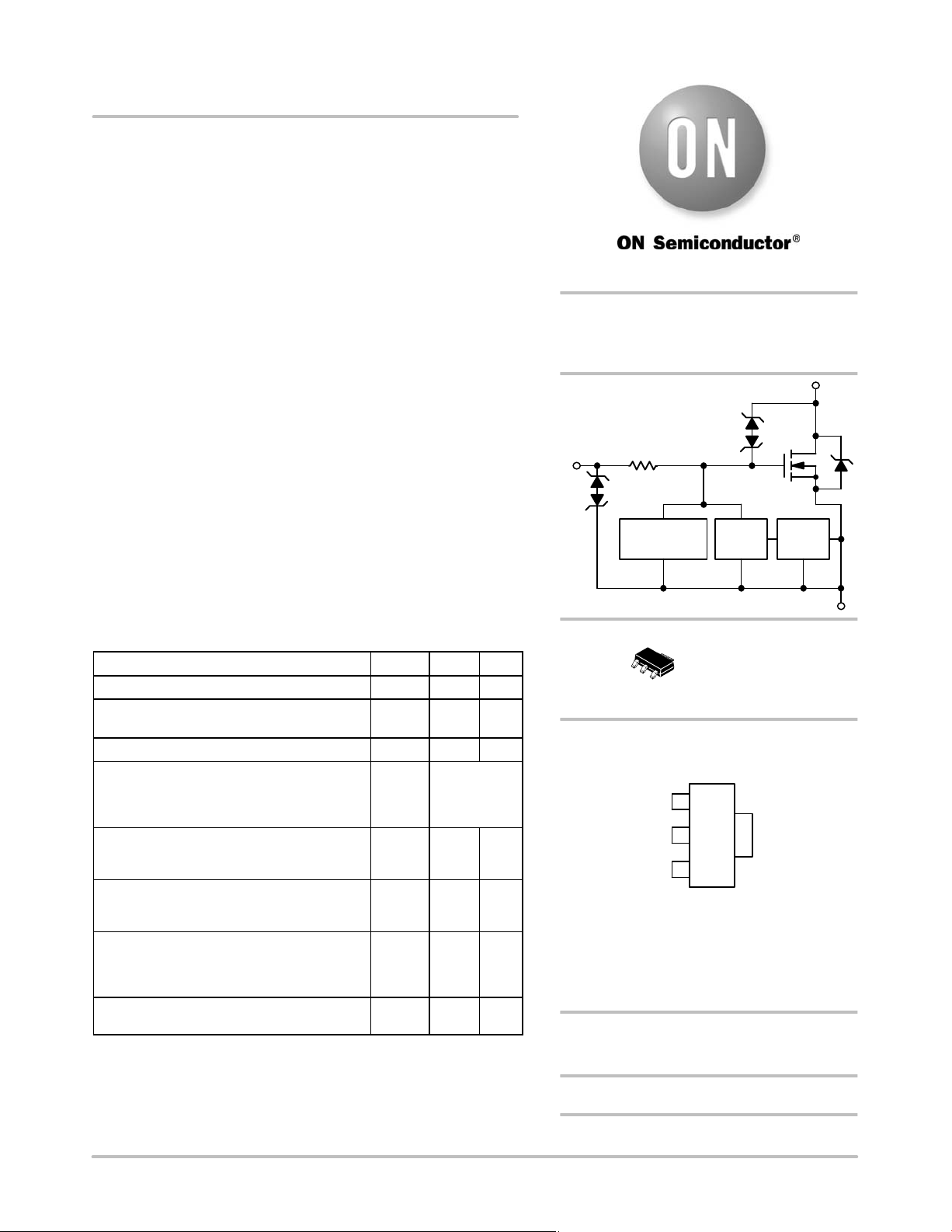
HDPlus devices are an advanced series of power MOSFETs which
utilize ON Semiconductor's latest MOSFET technology process to
achieve the lowest possible on-resistance per silicon area while
incorporating smart features. Integrated thermal and current limits
work together to provide short circuit protection. The devices feature
an integrated Drain-to-Gate Clamp that enables them to withstand
high energy in the avalanche mode. The Clamp also provides
additional safety margin against unexpected voltage transients.
Electrostatic Discharge (ESD) protection is provided by an integrated
Gate-to-Source Clamp.
Features
•Current Limitation
•Thermal Shutdown with Automatic Restart
•Short Circuit Protection
•Low R
•I
•Avalanche Energy Specified
•Slew Rate Control for Low Noise Switching
•Overvoltage Clamped Protection
•Pb-Free Packages are Available
DS(on)
Specified at Elevated Temperature
DSS
Gate
Input
http://onsemi.com
6.0 AMPERES*
40 VOLTS CLAMPED
R
DS(on)
R
G
ESD Protection
Temperature
Limit
= 90 mW
Overvoltage
Protection
Current
Limit
Drain
Current
Sense
Source
M
PWR
MOSFET MAXIMUM RATINGS (T
Rating Symbol Value Unit
Drain-to-Source Voltage Internally Clamped V
Drain-to-Gate Voltage Internally Clamped
= 1.0 MW)
(R
GS
Gate-to-Source Voltage V
Drain Current
- Continuous @ T
- Continuous @ TA = 100°C
- Pulsed (t
Total Power Dissipation @ TA = 25°C (Note 1)
@ T
@ TA = 25°C (Note 3)
Thermal Resistance, Junction-to-Tab
Junction-to-Ambient (Note 1)
Junction-to-Ambient (Note 2)
Single Pulse Drain-to-Source Avalanche Energy
(V
DD
VDS = 40 Vdc, IL = 2.8 Apk, L = 80 mH,
R
G
Operating and Storage Temperature Range TJ, T
Stresses exceeding Maximum Ratings may damage the device. Maximum
Ratings are stress ratings only. Functional operation above the Recommended
Operating Conditions is not implied. Extended exposure to stresses above the
Recommended Operating Conditions may affect device reliability.
1. Mounted onto min pad board.
2. Mounted onto 1″ pad board.
3. Mounted onto large heatsink.
p
= 25°C (Note 2)
A
= 25 Vdc, VGS = 5.0 Vdc,
= 25 W)
A
≤ 10 ms)
= 25°C
= 25°C unless otherwise noted)
J
JT
stg
40 Vdc
40 Vdc
"16 Vdc
Internally
Limited
1.1
1.73
8.93
14
114
72.3
300 mJ
-55 to
150
V
I
R
R
R
E
DSS
DGR
GS
I
D
I
D
DM
P
D
q
q
JA
q
JA
AS
W
°C/W
°C
4
1
2
3
SOT-223
CASE 318E
STYLE 3
MARKING DIAGRAM
GATE
DRAIN
SOURCE
A = Assembly Location
Y = Year
W = Work Week
62514 = Specific Device Code
G = Pb-Free Package
(Note: Microdot may be in either location)
1
4
62514G
AYW
2
G
3
DRAIN
ORDERING INFORMATION
See detailed ordering and shipping information in the package
dimensions section on page 5 of this data sheet.
Preferred devices are recommended choices for future use
and best overall value.
*Limited by the current limit circuit.
© Semiconductor Components Industries, LLC, 2007
November, 2007 - Rev. 6
1 Publication Order Number:
NIF62514/D
NIF62514
MOSFET ELECTRICAL CHARACTERISTICS (T
Characteristic
= 25°C unless otherwise noted)
J
Symbol Min Typ Max Unit
OFF CHARACTERISTICS
Drain-to-Source Clamped Breakdown Voltage
= 0 Vdc, ID = 250 mAdc)
(V
GS
= 0 Vdc, ID = 250 mAdc, TJ = 150°C)
(V
GS
Zero Gate Voltage Drain Current
(V
= 32 Vdc, VGS = 0 Vdc)
DS
(VDS = 32 Vdc, VGS = 0 Vdc, TJ = 150°C)
Gate Input Current
(V
= 5.0 Vdc, VDS = 0 Vdc)
GS
(VGS = -5.0 Vdc, VDS = 0 Vdc)
V
(BR)DSS
I
DSS
I
GSS
42
42
46
45
-
-
-
-
0.5
2.0
50
550
50
50
2.0
10
100
1000
ON CHARACTERISTICS
Gate Threshold Voltage
= VGS, ID = 150 mAdc)
(V
DS
Threshold Temperature Coefficient (Negative)
Static Drain-to-Source On-Resistance (Note 4)
(V
= 10 Vdc, ID = 1.4 Adc, TJ @ 25°C)
GS
(VGS = 10 Vdc, ID = 1.4 Adc, TJ @ 150°C)
Static Drain-to-Source On-Resistance (Note 4)
(V
= 5.0 Vdc, ID = 1.4 Adc, TJ @ 25°C)
GS
(VGS = 5.0 Vdc, ID = 1.4 Adc, TJ @ 150°C)
Source-Drain Forward On Voltage
(I
= 7 A, VGS = 0 V)
S
V
GS(th)
R
DS(on)
R
DS(on)
V
SD
1.0
-
-
-
-
-
1.7
4.0
90
165
105
185
2.0
6.0
100
190
120
210
- 1.05 - V
SWITCHING CHARACTERISTICS
Turn-on Delay Time 10% Vin to 10% I
RL = 4.7 W, Vin = 0 to 10 V, VDD = 12 V
Turn-on Rise Time 10% ID to 90% I
RL = 4.7 W, Vin = 0 to 10 V, VDD = 12 V
Turn-off Delay Time 90% Vin to 90% I
RL = 4.7 W, Vin = 10 to 0 V, VDD = 12 V
Turn-off Fall Time 90% ID to 10% I
RL = 4.7 W, Vin = 10 to 0 V, VDD = 12 V
Slew-Rate On
RL = 4.7 W,
Vin = 0 to 10 V, VDD = 12 V
Slew-Rate Off
RL = 4.7 W,
V
= 10 to 0 V, VDD = 12 V
in
D
D
D
D
t
d(on)
t
rise
t
d(off)
t
fall
-dVDS/dt
dVDS/dt
- 4.0 8.0
- 11 20
- 32 50
- 27 50
- 1.5 2.5
on
off
- 0.6 1.0
SELF PROTECTION CHARACTERISTICS (TJ = 25°C unless otherwise noted)
Current Limit
Current Limit (VGS = 10 Vdc)
Temperature Limit (Turn-off) VGS = 5.0 Vdc T
Temperature Limit (Circuit Reset) VGS = 5.0 Vdc T
Temperature Limit (Turn-off) VGS = 10 Vdc T
Temperature Limit (Circuit Reset) VGS = 10 Vdc T
(VGS = 5.0 Vdc)
(V
= 5.0 Vdc, TJ = 150°C)
GS
(V
= 10 Vdc, TJ = 150°C)
GS
I
LIM
I
LIM
LIM(off)
LIM(on)
LIM(off)
LIM(on)
6.0
3.0
7.0
4.0
9.0
5.0
10.5
7.5
11
8.0
13
10
150 175 200 °C
135 160 185 °C
150 155 185 °C
130 140 170 °C
ESD ELECTRICAL CHARACTERISTICS (TJ = 25°C unless otherwise noted)
Electro-Static Discharge Capability
Human Body Model (HBM) ESD 4000 - - V
Electro-Static Discharge Capability Machine Model (MM) ESD 400 - - V
4. Pulse Test: Pulse Width = 300 ms, Duty Cycle = 2%.
Vdc
mAdc
mAdc
Vdc
mV/°C
mW
mW
ms
ms
ms
ms
ms
ms
Adc
Adc
http://onsemi.com
2
 Loading...