

Page 1
N-Channel Logic Level
Enhancement Mode Field
Effect Transistor
NDS331N
General Description
These N−Channel logic level enhancement mode power field effect
transistors are produced using ON Semiconductor’s proprietary, high
cell density, DMOS technology. This very high density process is
especially tailored to minimize on−state resistance. These devices are
particularly suited for low voltage applications in notebook
computers, portable phones, PCMCIA cards, and other battery
powered circuits where fast switching, and low in−line power loss are
needed in a very small outline surface mount package.
Features
• 1.3 A, 20 V
♦ R
♦ R
= 0.21 @ VGS = 2.7 V
DS(on)
= 0.16 @ VGS = 4.5 V
DS(on)
• Industry Standard Outline SOT−23 Surface Mount Package Using
Poprietary SUPERSOTt−3 Design for Superior Thermal and
Electrical Capabilities
• High Density Cell Design for Extremely Low R
DS(on)
• Exceptional On−Resistance and Maximum DC Current Capability
• This is a Pb−Free Device
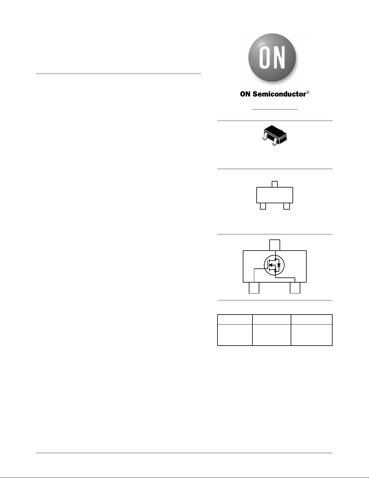
www.onsemi.com
D
G
S
SOT−23/SUPERSOT−23, 3 LEAD, 1.4x2.9
CASE 527AG
MARKING DIAGRAM
&Y
331 &G
&Y = Binary Calendar Year Coding Scheme
331 = Specific Device Code
&G = Date Code
D
© Semiconductor Components Industries, LLC, 2017
April, 2021 − Rev. 6
G
ORDERING INFORMATION
Device Package Shipping
NDS331N SOT−23−3/
SUPERSOT−23
(Pb−Free)
†For information on tape and reel specifications,
including part orientation and tape sizes, please
refer to our Tape and Reel Packaging Specifications
Brochure, BRD8011/D.
1 Publication Order Number:
S
†
3000 /
Tape & Reel
NDS331N/D
Page 2
NDS331N
ABSOLUTE MAXIMUM RATINGS T
Symbol
V
V
DSS
GSS
I
D
Drain−Source Voltage 20 V
Gate−Source Voltage − Continuous ±8 V
Maximum Drain Current – Continuous (Note 1a) 1.3
= 25°C unless otherwise noted.
A
Parameter Ratings Unit
A
Maximum Drain Current – Pulsed 10
P
Maximum Power Dissipation (Note 1a) 0.5
D
W
Maximum Power Dissipation (Note 1b) 0.46
TJ, T
Operating and Storage Temperature Range −55 to +150 °C
STG
Stresses exceeding those listed in the Maximum Ratings table may damage the device. If any of these limits are exceeded, device functionality
should not be assumed, damage may occur and reliability may be affected.
THERMAL CHARACTERISTICS
Symbol Parameter Ratings Unit
R
R
1. R
JA
mounting surface of the drain pins. R
(t) +
P
D
Typical R
Thermal Resistance, Junction−to−Ambient (Note 1a) 250 °C/W
JA
Thermal Resistance, Junction−to−Case (Note 1) 75 °C/W
JC
is the sum of the junction−to−case and case−to−ambient thermal resistance where the case thermal reference is defined as the solder
is guaranteed by design while R
JC
T
* T
J
R
(t)
JA
using the board layouts shown below on 4.5″x5″ FR−4 PCB in a still air environment:
JA
a) 250°C/W when mounted on a 0.02 in
T
A
+
* T
J
A
R
) R
JC
CA
2
+ I
(t) R
DS(on)@T
D
(t)
2
pad
J
of 2oz copper.
is determined by the user’s board design.
CA
b) 270°C/W when mounted on a 0.001 in2 pad
of 2oz copper.
Scale 1:1 on letter size paper
www.onsemi.com
2
Page 3
NDS331N
ELECTRICAL CHARACTERISTICS T
Symbol
Parameter Test Conditions Min Typ Max Unit
= 25°C unless otherwise noted.
A
OFF CHARACTERISTICS
BV
I
DSS
Drain–Source Breakdown Voltage
DSS
Zero Gate Voltage Drain Current
VGS = 0 V, ID = 250 A
VDS = 16 V, VGS = 0 V − − 1 A
20 − − V
VDS = 16 V, VGS = 0 V, TJ = 125°C − − 10
I
GSSF
I
GSSR
Gate–Body Leakage, Forward VGS = 8 V, VDS = 0 V − − 100 nA
Gate–Body Leakage, Reverse VGS = −8 V, VDS = 0 V − − −100 nA
ON CHARACTERISTICS (Note 2)
V
GS(th)
R
DS(on)
Gate Threshold Voltage
Static Drain–Source On–Resistance
VDS = VGS, ID = 250 A
VDS = VGS, ID = 250 A, TJ = 125°C
0.5 0.7 1
0.3 0.53 0.8
VGS = 2.7 V, ID = 1.3 A − 0.15 0.21
V
VGS = 2.7 V, ID = 1.3 A, TJ = 125°C − 0.24 0.4
VGS = 4.5 V, ID = 1.5 A − 0.11 0.16
I
D(on)
On–State Drain Current
VGS = 2.7 V, VDS = 5 V 3 − −
A
VGS = 4.5 V, VDS = 5 V 4 − −
g
Forward Transconductance VDS = 5 V, ID = 1.3 A − 3.5 − S
FS
DYNAMIC CHARACTERISTICS
C
C
C
Input Capacitance
iss
Output Capacitance − 85 − pF
oss
Reverse Transfer Capacitance − 28 − pF
rss
VDS = 10 V, VGS = 0 V, f = 1.0 MHz
− 162 − pF
SWITCHING CHARACTERISTICS (Note 2)
t
D(on)
t
t
D(off)
t
Q
Q
Q
Turn–On Delay Time
Turn–On Rise Time − 25 40 ns
r
Turn–Off Delay Time − 10 20 ns
Turn–Off Fall Time − 5 20 ns
f
Total Gate Charge
g
Gate–Source Charge − 0.3 − nC
gs
Gate–Drain Charge − 1 − nC
gd
VDD = 5 V, ID = 1 A, VGS = 5 V,
= 6
R
GEN
VDS = 5 V, ID = 1.3 A, VGS = 4.5 V
− 5 20 ns
− 3.5 5 nC
DRAIN−SOURCE DIODE CHARACTERISTICS AND MAXIMUM RATINGS
Maximum Continuous Drain–Source Diode Forward Current − − 0.42 A
I
S
I
SM
V
Maximum Pulsed Drain−Source Diode Forward Current − − 10 A
Drain–Source Diode Forward Voltage VGS = 0 V, IS = 0.42 A (Note 2) − 0.8 1.2 V
SD
Product parametric performance is indicated in the Electrical Characteristics for the listed test conditions, unless otherwise noted. Product
performance may not be indicated by the Electrical Characteristics if operated under different conditions.
2. Pulse Test: Pulse Width ≤ 300 s, Duty Cycle ≤ 2.0%.
www.onsemi.com
3
Page 4

NDS331N
TYPICAL ELECTRICAL CHARACTERISTICS
4
3
2
1
, Drain−Source Current (A)
D
I
0
0
Figure 1. On−Region Characteristics Figure 2. On−Resistance Variation with
1.8
ID = 1.3 A
V
GS
1.6
1.4
1.2
, Normalized
1
DS(on)
R
0.8
Drain−Source On−Resistance
VGS = 4.5 V
3.0
2.7
2.5
123
VDS, Drain−Source Voltage (V)
= 2.7 V
2.0
1.5
1.75
1.5
VGS = 2.0 V
1.25
, Normalized
1
DS(on)
R
0.75
Drain−Source On−Resistance
2.5
2.7 3.0
0.5
021 1.5 2.5 3
0.5
I
, Drain Current (A)
D
Drain Current and Gate Voltage
1.75
1.25
, Normalized
DS(on)
R
0.75
Drain−Source On−Resistance
1.5
1
VGS = 2.7 V
TJ = 125°C
25°C
−55°C
3.5
4.5
0.6
−50 −25 0 25 50 75 100 125 150
Figure 3. On−Resistance Variation with
Temperature
4
VDS = 5.0 V
3
2
, Drain Current (A)
D
I
1
0
0 0.5 1 1.5 2
VGS, Gate To Source Voltage (V)
TJ = −55°C
25°C
125°C
2.5 3
Figure 5. Transfer Characteristics Figure 6. Gate Threshold Variation with
0.5
0 0.5 1 1.5 2
I
, Drain Current (A)TJ, Junction Temperature (°C)
D
Figure 4. On−Resistance Variation with
Drain Current and Temperature
1.3
1.2
VDS = V
ID = 250 A
1.1
1
0.9
0.8
Threshold Voltage
0.7
, Normalized Gate−Source
th
V
0.6
0.5
−50 −25 0 25 50 75 100 125 150
T
, Junction Temperature (°C)
J
Temperature
2.5 3
GS
www.onsemi.com
4
Page 5

NDS331N
2
TYPICAL ELECTRICAL CHARACTERISTICS (continued)
1.12
ID = 250 A
1.08
1.04
1
Breakdown Voltage
, Normalized Drain−Source
0.96
DSS
BV
0.92
−50 −25 0 25 50 75 100 125 150
TJ, Junction Temperature (°C)
Figure 7. Breakdown Voltage Variation with
Temperature
600
400
200
100
1
VGS = 0 V
0.1
0.01
TJ = 125°C
0.001
, Reverse Drain Current (A)
S
I
25°C
−55°C
0.0001
0 0.2 0.4 0.6 0.8
1
1.
VSD, Body Diode Forward Voltage (V)
Figure 8. Body Diode Forward Voltage Variation
with Source Current and Temperature
5
ID = 1.3 A
C
iss
C
oss
4
3
VDS = 5 V
10 V
15 V
50
Capacitance (pF)
20
f = 1 MHz
= 0 V
V
GS
10
0.1 0.5
2 5 10 20
VDS, Drain−Source Voltage (V)
C
rss
2
, Gate−Source Voltage (V)
1
GS
V
0
0123 410.2
Q
, Gate Charge (nC)
g
Figure 9. Capacitance Characteristics Figure 10. Gate Charge Characteristics
V
DD
t
V
IN
V
GS
R
GEN
G
R
L
D
V
OUT
DUT
S
d(on)
V
V
OUT
IN
10%
t
on
10%
50%
t
r
90%
Pulse Width
t
d(off)
Figure 11. Switching Test Circuit Figure 12. Switching Waveforms
50%
90%
t
off
90%
10%
t
f
Inverted
5
www.onsemi.com
5
Page 6

NDS331N
TYPICAL ELECTRICAL CHARACTERISTICS (continued)
8
V
= 5.0 V
DS
6
TJ = −55°C
4
125°C
2
, Transconductance (Siemens)
FS
g
0
02
ID, Drain Current (A)
Figure 13. Transconductance Variation with Drain
Current and Temperature
1
0.8
0.6
1a
1b
0.4
0.2
Steady−State Power Dissipation (W)
0
0 0.2
2oz Copper Mounting Pad Area (in2)
4.5″x5″ FR−4 Board
= 25°C
T
A
Still Air
25°C
0.4
50
This Area is Limited by r
DS(on)
10
100 s
1 ms
1
10 ms
, Drain Current (A)
D
I
0.1
0.01
Single Pulse
= Max Rated
T
J
R
= 270°C/W
JA
T
= 25°C
A
Curve Bent to
Measured Date
4 0.1 1 1031
, Drain to Source Voltage (V)
V
DS
100 ms
60
Figure 14. Maximum Safe Operating Area
1.8
1.6
1.4
1a
1.2
1b
, Steady−State Drain Current (A)
D
I
1
0 0.1 0.2 0.30.30.1
2oz Copper Mounting Pad Area (in
4.5″x5″ FR−4 Board
= 25°C
T
A
Still Air
V
= 2.7 V
GS
2
)
0.4
Figure 15. SUPERSOT−3 Maximum Steady−State
Power Dissipation versus Copper Mounting Pad Area
2
1
0.1
0.01
, Normalized Thermal Impedance
JA
Z
0.001
10
Duty Cycle−Descending Order
D = 0.5
0.2
0.1
0.05
0.02
0.01
Single Pulse
−4
10
−3
10
−2
10
−1
t, Rectangular Pulse Duration (s)
Figure 17. Transient Thermal Response Curve
NOTE: Thermal characterization performed using the conditions described in
Note 1b. Response will change depending on the circuit board design.
www.onsemi.com
Figure 16. Maximum Steady−State Drain
Current versus Copper Mounting Pad Area
P
DM
t
1
t
NOTES:
Z
(t)= r(t) x R
JA
R
= 270°C/W
JA
Peak T
= PDM x Z
J
Duty Cycle, D = t1 / t
1 10 100
6
2
JA
(t) + T
A
JA
2
1000
Page 7

NDS331N
SUPERSOT is a trademark of Semiconductor Components Industries, LLC (SCILLC) or its subsidiaries in the United States and/or other countries.
www.onsemi.com
7
Page 8

MECHANICAL CASE OUTLINE
PACKAGE DIMENSIONS
SOT−23/SUPERSOTt−23, 3 LEAD, 1.4x2.9
CASE 527AG
ISSUE A
DATE 09 DEC 2019
GENERIC
MARKING DIAGRAM*
XXXMG
G
DOCUMENT NUMBER:
DESCRIPTION:
ON Semiconductor and are trademarks of Semiconductor Components Industries, LLC dba ON Semiconductor or its subsidiaries in the United States and/or other countries.
ON Semiconductor reserves the right to make changes without further notice to any products herein. ON Semiconductor makes no warranty, representation or guarantee regarding
the suitability of its products for any particular purpose, nor does ON Semiconductor assume any liability arising out of the application or use of any product or circuit, and specifically
disclaims any and all liability, including without limitation special, consequential or incidental damages. ON Semiconductor does not convey any license under its patent rights nor the
rights of others.
© Semiconductor Components Industries, LLC, 2019
98AON34319E
SOT−23/SUPERSOT−23, 3 LEAD, 1.4X2.9
XXX = Specific Device Code
M = Month Code
G = Pb−Free Package
(Note: Microdot may be in either location)
Electronic versions are uncontrolled except when accessed directly from the Document Repository.
Printed versions are uncontrolled except when stamped “CONTROLLED COPY” in red.
*This information is generic. Please refer to
device data sheet for actual part marking.
Pb−Free indicator, “G” or microdot “G”, may
or may not be present. Some products may
not follow the Generic Marking.
PAGE 1 OF 1
www.onsemi.com
Page 9

ON Semiconductor and are trademarks of Semiconductor Components Industries, LLC dba ON Semiconductor or its subsidiaries in the United States and/or other countries.
ON Semiconductor owns the rights to a number of patents, trademarks, copyrights, trade secrets, and other intellectual property. A listing of ON Semiconductor’s product/patent
coverage may be accessed at www.onsemi.com/site/pdf/Patent−Marking.pdf
ON Semiconductor makes no warranty, representation or guarantee regarding the suitability of its products for any particular purpose, nor does ON Semiconductor assume any liability
arising out of the application or use of any product or circuit, and specifically disclaims any and all liability, including without limitation special, consequential or incidental damages.
Buyer is responsible for its products and applications using ON Semiconductor products, including compliance with all laws, regulations and safety requirements or standards,
regardless of any support or applications information provided by ON Semiconductor. “Typical” parameters which may be provided in ON Semiconductor data sheets and/or
specifications can and do vary in different applications and actual performance may vary over time. All operating parameters, including “Typicals” must be validated for each customer
application by customer’s technical experts. ON Semiconductor does not convey any license under its patent rights nor the rights of others. ON Semiconductor products are not
designed, intended, or authorized for use as a critical component in life support systems or any FDA Class 3 medical devices or medical devices with a same or similar classification
in a foreign jurisdiction or any devices intended for implantation in the human body. Should Buyer purchase or use ON Semiconductor products for any such unintended or unauthorized
application, Buyer shall indemnify and hold ON Semiconductor and its officers, employees, subsidiaries, affiliates, and distributors harmless against all claims, costs, damages, and
expenses, and reasonable attorney fees arising out of, directly or indirectly, any claim of personal injury or death associated with such unintended or unauthorized use, even if such
claim alleges that ON Semiconductor was negligent regarding the design or manufacture of the part. ON Semiconductor is an Equal Opportunity/Affirmative Action Employer. This
literature is subject to all applicable copyright laws and is not for resale in any manner.
. ON Semiconductor reserves the right to make changes without further notice to any products herein.
PUBLICATION ORDERING INFORMATION
LITERATURE FULFILLMENT:
Email Requests to: orderlit@onsemi.com
ON Semiconductor Website: www.onsemi.com
TECHNICAL SUPPORT
North American Technical Support:
Voice Mail: 1 800−282−9855 Toll Free USA/Canada
Phone: 011 421 33 790 2910
Europe, Middle East and Africa Technical Support:
Phone: 00421 33 790 2910
For additional information, please contact your local Sales Representative
◊
www.onsemi.com
1
 Loading...