

Page 1
NDF06N60Z
Power MOSFET, N-Channel,
00 V, 1.2 W
6
Features
• Low ON Resistance
• Low Gate Charge
• ESD Diode−Protected Gate
• 100% Avalanche Tested
• These Devices are Pb−Free, Halogen Free/BFR Free and are RoHS
Compliant
ABSOLUTE MAXIMUM RATINGS (T
Rating
Drain−to−Source Voltage V
Continuous Drain Current, R
Continuous Drain Current
T
= 100°C, R
A
Pulsed Drain Current,
V
@ 10 V
GS
Power Dissipation, R
Gate−to−Source Voltage V
Single Pulse Avalanche Energy, L = 6.3 mH,
I
= 6.0 A
D
ESD (HBM) (JESD22−A114) V
RMS Isolation Voltage
(t = 0.3 sec., R.H. ≤ 30%,
T
= 25°C) (Figure 13)
A
Peak Diode Recovery (Note 2) dv/dt 4.5 V/ns
MOSFET dV/dt dV/dt 60 V/ns
Continuous Source Current (Body Diode) I
Maximum Temperature for Soldering Leads T
Operating Junction and
Storage Temperature Range
Stresses exceeding those listed in the Maximum Ratings table may damage the
device. If any of these limits are exceeded, device functionality should not be
assumed, damage may occur and reliability may be affected.
1. Limited by maximum junction temperature
= 6.0 A, di/dt ≤ 100 A/ms, VDD ≤ BV
2. I
SD
(Note 1)
q
JC
q
JC
(Note 1)
q
JC
= 25°C unless otherwise noted)
C
Symbol Value Unit
stg
600 V
7.1 A
4.5 A
28 A
35 W
±30 V
113 mJ
3000 V
4500 V
6.0 A
260 °C
−55 to
150
, TJ = +150°C
DSS
DSS
I
I
I
DM
P
E
V
TJ, T
D
D
D
GS
AS
esd
ISO
S
L
°C
www.onsemi.com
V
DSS
(@ T
650 V
G (1)
)R
Jmax
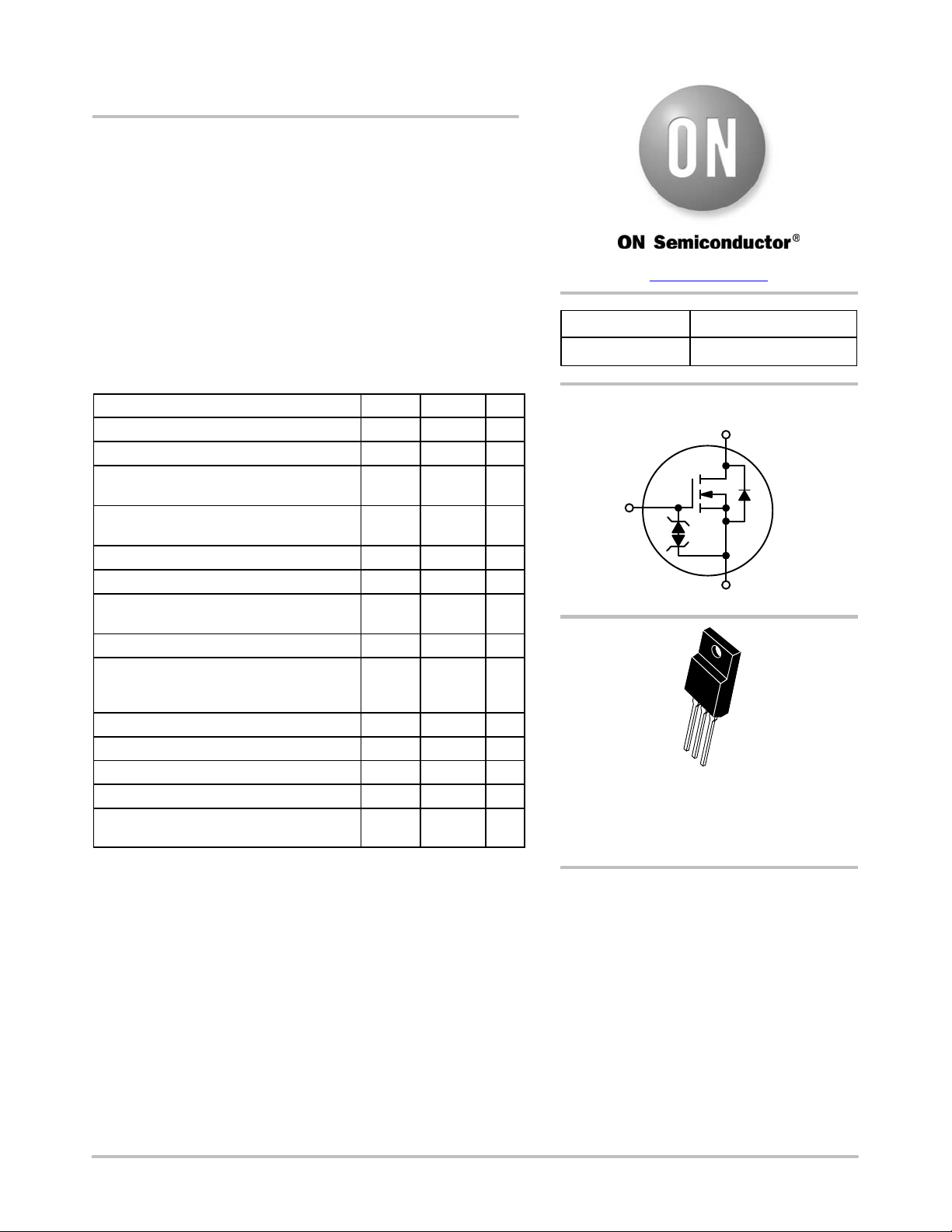
N−Channel
D (2)
1
2
3
NDF06N60ZG,
NDF06N60ZH
TO−220FP
CASE 221AH
DS(ON)
S (3)
(MAX) @ 3 A
1.2 Ω
ORDERING AND MARKING INFORMATION
See detailed ordering, marking and shipping information on
page 6 of this data sheet.
© Semiconductor Components Industries, LLC, 2015
January, 2015 − Rev. 8
1 Publication Order Number:
NDF06N60Z/D
Page 2
THERMAL RESISTANCE
Parameter Symbol Value Unit
Junction−to−Case (Drain)
Junction−to−Ambient Steady State (Note 3)
3. Insertion mounted
NDF06N60Z
R
q
JC
R
q
JA
3.6
50
°C/W
ELECTRICAL CHARACTERISTICS (T
Characteristic
= 25°C unless otherwise noted)
J
Test Conditions Symbol Min Typ Max Unit
OFF CHARACTERISTICS
Drain−to−Source Breakdown Voltage VGS = 0 V, ID = 1 mA BV
Breakdown Voltage Temperature Co-
efficient
Drain−to−Source Leakage Current
Reference to 25°C,
= 1 mA
I
D
VDS = 600 V, VGS = 0 V
DBV
25°C
150°C 50
Gate−to−Source Forward Leakage VGS = ±20 V I
DT
I
DSS
GSS
DSS
DSS
J
600 V
/
0.6 V/°C
1 mA
±10
mA
ON CHARACTERISTICS (Note 4)
Static Drain−to−Source
VGS = 10 V, ID = 3.0 A R
DS(on)
0.98 1.2
W
On−Resistance
Gate Threshold Voltage
VDS = VGS, ID = 100 mA
Forward Transconductance VDS = 15 V, ID = 3.0 A g
V
GS(th)
FS
3.0 3.9 4.5 V
5.0 S
DYNAMIC CHARACTERISTICS
Input Capacitance (Note 5)
Output Capacitance (Note 5) C
Reverse Transfer Capacitance
VDS = 25 V, VGS = 0 V,
f = 1.0 MHz
C
iss
oss
C
rss
738 923 1107
90 106 125
15 23 30
pF
(Note 5)
Total Gate Charge (Note 5)
Gate−to−Source Charge (Note 5) Q
Gate−to−Drain (“Miller”) Charge
(Note 5)
VDD = 300 V, ID = 6.0 A,
= 10 V
V
GS
Plateau Voltage V
Gate Resistance R
Q
g
gs
Q
gd
GP
g
15.5 31 47
3 6.3 9.5
8 17 24.5
6.4 V
3.2
nC
W
RESISTIVE SWITCHING CHARACTERISTICS
Turn−On Delay Time
Rise Time t
Turn−Off Delay Time t
V
= 300 V, ID = 6.0 A,
DD
= 10 V, RG = 5 Ω
V
GS
t
Fall Time t
d(on)
r
d(off)
f
13
17
30
28
ns
SOURCE−DRAIN DIODE CHARACTERISTICS (TC = 25°C unless otherwise noted)
Diode Forward Voltage IS = 6.0 A, VGS = 0 V V
Reverse Recovery Time
Reverse Recovery Charge Q
VGS = 0 V, VDD = 30 V
I
= 6.0 A, di/dt = 100 A/ms
S
SD
t
rr
rr
338 ns
2.0
1.6 V
mC
Product parametric performance is indicated in the Electrical Characteristics for the listed test conditions, unless otherwise noted. Product
performance may not be indicated by the Electrical Characteristics if operated under different conditions.
4. Pulse Width ≤ 380 ms, Duty Cycle ≤ 2%.
5. Guaranteed by design.
www.onsemi.com
2
Page 3
NDF06N60Z
TYPICAL CHARACTERISTICS
12
TJ = 25°C
10
8
6
4
, DRAIN CURRENT (A)
D
I
2
0
VGS = 15 V
VDS, DRAIN−TO−SOURCE VOLTAGE (V) VGS, GATE−TO−SOURCE VOLTAGE (V)
Figure 1. On−Region Characteristics Figure 2. Transfer Characteristics
2
1.5
1
10 V
7 V
6.8 V
20
ID = 3 A
= 25°C
T
J
6.6 V
6.4 V
6.2 V
6.0 V
5.8 V
5.6 V
12
10
8
6
4
, DRAIN CURRENT (A)
D
I
2
25151050
0
1.75
1.5
1.25
1
VDS ≥ 30 V
TJ = 25°C
TJ = 150°C
VGS = 10 V
TJ = −55°C
6
TJ = 25°C
87543
0.5
, DRAIN−TO−SOURCE RESISTANCE (W)
0
DS(on)
R
Figure 3. On−Resistance vs. V
2.6
ID = 3 A
= 10 V
V
GS
2.2
1.8
1.4
1.0
, DRAIN−TO−SOURCE RES-
ISTANCE (NORMALIZED)
0.6
DS(on)
R
0.2
TJ, JUNCTION TEMPERATURE (°C) VDS, DRAIN−TO−SOURCE VOLTAGE (V)
Figure 5. On−Resistance Variation with
0.75
, DRAIN−TO−SOURCE RESISTANCE (W)
9871065
VGS (V) ID, DRAIN CURRENT (A)
GS
DS(on)
R
0.5
Figure 4. On−Resistance vs. Drain Current and
Gate Voltage
50
10,000
, LEAKAGE (nA)
DSS
I
15012510075250−25−50
1000
100
10
VGS = 0 V
TJ = 150°C
TJ = 100°C
Figure 6. Drain−to−Source Leakage Current
Temperature
vs. Voltage
106212840
500
6004003002001000
www.onsemi.com
3
Page 4

NDF06N60Z
TYPICAL CHARACTERISTICS
2000
1500
1000
500
C, CAPACITANCE (pF)
0
1000
VDD = 300 V
I
V
100
t, TIME (ns)
10
20
VGS = 0 V
= 25°C
T
J
f = 1 MHz
15
V
C
iss
10
Qgs
C
oss
C
rss
200150100500
5
, GATE−TO−SOURCE VOLTAGE (V)
GS
0
V
QT
DS
Qgd
15
VDS, DRAIN−TO−SOURCE VOLTAGE (V) Qg, TOTAL GATE CHARGE (nC)
Figure 7. Capacitance Variation Figure 8. Gate−to−Source and
Drain−to−Source Voltage vs. Total Charge
6
= 6 A
D
GS
= 10 V
t
d(off)
t
r
t
f
t
d(on)
, SOURCE CURRENT (A)
S
I
5
4
3
2
1
VGS = 0 V
TJ = 25°C
V
GS
TJ = 25°C
= 6 A
I
D
V
400
DS
, DRAIN−TO−SOURCE VOLTAGE (V)
300
200
100
0
353025201050
1
RG, GATE RESISTANCE (W)
Figure 9. Resistive Switching Time Variation
vs. Gate Resistance
100
VGS ≤ 30 V
Single Pulse
T
= 25°C
C
10
1
0.1
, DRAIN CURRENT (A)
D
I
0.01
1
VDS, DRAIN−TO−SOURCE VOLTAGE (V)
Figure 11. Maximum Rated Forward Biased
Safe Operating Area for NDF06N60Z
100101
10 ms
dc
R
Limit
DS(on)
Thermal Limit
Package Limit
100 ms
1 ms
0
V
, SOURCE−TO−DRAIN VOLTAGE (V)
SD
Figure 10. Diode Forward Voltage vs. Current
10 ms
1000100100.1
0.90.80.7 1.00.60.50.4
www.onsemi.com
4
Page 5

10
1.0
R(t) (C/W)
0.1
NDF06N60Z
TYPICAL CHARACTERISTICS
50% (DUTY CYCLE)
20%
10%
5.0%
2.0%
1.0%
0.01
SINGLE PULSE
0.0001 0.001 0.01 1.0 10 1000.000001
PULSE TIME (s)
0.10.00001
Figure 12. Thermal Impedance for NDF06N60Z
LEADS
HEATSINK
0.110″ MIN
Figure 13. Mounting Position for Isolation Test
Measurement made between leads and heatsink with all leads shorted together.
*For additional mounting information, please download the ON Semiconductor
Soldering and Mounting Techniques Reference Manual, SOLDERRM/D.
R
= 3.6°C/W
q
JC
Steady State
1000
www.onsemi.com
5
Page 6

NDF06N60Z
ORDERING INFORMATION
Order Number Package Shipping
NDF06N60ZG TO−220FP
(Pb−Free, Halogen−Free)
NDF06N60ZH TO−220FP
(Pb−Free, Halogen−Free)
†For information on tape and reel specifications, including part orientation and tape sizes, please refer to our Tape and Reel Packaging
Specifications Brochure, BRD8011/D.
50 Units / Rail
50 Units / Rail
MARKING DIAGRAMS
NDF06N60ZG
or
NDF06N60ZH
AYWW
Gate Source
†
Drain
TO−220FP
A = Location Code
Y = Year
WW = Work Week
G, H = Pb−Free, Halogen−Free Package
www.onsemi.com
6
Page 7

MECHANICAL CASE OUTLINE
PACKAGE DIMENSIONS
TO−220 FULLPACK, 3−LEAD
CASE 221AH
ISSUE F
DATE 30 SEP 2014
SCALE 1:1
E
E/2
Q
123
L
3X
b2
L1
P
M
0.14
D
C
3X
b
0.25
M
M
AB
e
FRONT VIEW
SECTION D−D
A
NOTE 6
DD
AAB
C
NOTE 6
SEATING
B
PLANE
H1
M
A
A1
NOTE 3
c
A2
SIDE VIEW
NOTES:
1. DIMENSIONING AND TOLERANCING PER ASME
Y14.5M, 1994.
2. CONTROLLING DIMENSION: MILLIMETERS.
3. CONTOUR UNCONTROLLED IN THIS AREA.
4. DIMENSIONS D AND E DO NOT INCLUDE MOLD FLASH AND GATE
PROTRUSIONS. MOLD FLASH AND GATE PROTRUSIONS NOT TO
EXCEED 0.13 PER SIDE. THESE DIMENSIONS ARE TO BE MEA
SURED AT OUTERMOST EXTREME OF THE PLASTIC BODY.
5. DIMENSION b2 DOES NOT INCLUDE DAMBAR PROTRUSION.
LEAD WIDTH INCLUDING PROTRUSION SHALL NOT EXCEED 2.00.
6. CONTOURS AND FEATURES OF THE MOLDED PACKAGE BODY
MAY VARY WITHIN THE ENVELOP DEFINED BY DIMENSIONS A1
AND H1 FOR MANUFACTURING PURPOSES.
MILLIMETERS
DIM MIN MAX
A 4.30 4.70
A1 2.50 2.90
A2 2.50 2.90
b 0.54 0.84
b2 1.10 1.40
c 0.49 0.79
D 14.70 15.30
E 9.70 10.30
e
2.54 BSC
H1 6.60 7.10
L 12.50 14.73
L1 --- 2.80
P 3.00 3.40
Q 2.80 3.20
GENERIC
MARKING DIAGRAM*
H1
XXXXXXXXX
XX
AWLYWWG
A
SECTION A−A
ALTERNATE CONSTRUCTION
1
A = Assembly Location
WL = Wafer Lot
Y = Year
WW = Work Week
STYLE 1:
PIN 1. MAIN TERMINAL 1
2. MAIN TERMINAL 2
3. GATE
STYLE 2:
PIN 1. CATHODE
2. ANODE
3. GATE
G = Pb−Free Package
*This information is generic. Please refer to
device data sheet for actual part marking.
Pb−Free indicator, “G” or microdot “ G”,
may or may not be present.
DOCUMENT NUMBER:
DESCRIPTION:
ON Semiconductor and are trademarks of Semiconductor Components Industries, LLC dba ON Semiconductor or its subsidiaries in the United States and/or other countries.
ON Semiconductor reserves the right to make changes without further notice to any products herein. ON Semiconductor makes no warranty, representation or guarantee regarding
the suitability of its products for any particular purpose, nor does ON Semiconductor assume any liability arising out of the application or use of any product or circuit, and specifically
disclaims any and all liability, including without limitation special, consequential or incidental damages. ON Semiconductor does not convey any license under its patent rights nor the
rights of others.
98AON52577E
TO−220 FULLPACK, 3−LEAD
Electronic versions are uncontrolled except when accessed directly from the Document Repository.
Printed versions are uncontrolled except when stamped “CONTROLLED COPY” in red.
PAGE 1 OF 1
© Semiconductor Components Industries, LLC, 2019
www.onsemi.com
Page 8

ON Semiconductor and are trademarks of Semiconductor Components Industries, LLC dba ON Semiconductor or its subsidiaries in the United States and/or other countries.
ON Semiconductor owns the rights to a number of patents, trademarks, copyrights, trade secrets, and other intellectual property. A listing of ON Semiconductor ’s product/patent
coverage may be accessed at www.onsemi.com/site/pdf/Patent−Marking.pdf
ON Semiconductor makes no warranty, representation or guarantee regarding the suitability of its products for any particular purpose, nor does ON Semiconductor assume any liability
arising out of the application or use of any product or circuit, and specifically disclaims any and all liability, including without limitation special, consequential or incidental damages.
Buyer is responsible for its products and applications using ON Semiconductor products, including compliance with all laws, regulations and safety requirements or standards,
regardless of any support or applications information provided by ON Semiconductor. “Typical” parameters which may be provided in ON Semiconductor data sheets and/or
specifications can and do vary in different applications and actual performance may vary over time. All operating parameters, including “Typicals” must be validated for each customer
application by customer’s technical experts. ON Semiconductor does not convey any license under its patent rights nor the rights of others. ON Semiconductor products are not
designed, intended, or authorized for use as a critical component in life support systems or any FDA Class 3 medical devices or medical devices with a same or similar classification
in a foreign jurisdiction or any devices intended for implantation in the human body. Should Buyer purchase or use ON Semiconductor products for any such unintended or unauthorized
application, Buyer shall indemnify and hold ON Semiconductor and its officers, employees, subsidiaries, affiliates, and distributors harmless against all claims, costs, damages, and
expenses, and reasonable attorney fees arising out of, directly or indirectly, any claim of personal injury or death associated with such unintended or unauthorized use, even if such
claim alleges that ON Semiconductor was negligent regarding the design or manufacture of the part. ON Semiconductor is an Equal Opportunity/Affirmative Action Employer. This
literature is subject to all applicable copyright laws and is not for resale in any manner.
. ON Semiconductor reserves the right to make changes without further notice to any products herein.
PUBLICATION ORDERING INFORMATION
LITERATURE FULFILLMENT:
Email Requests to: orderlit@onsemi.com
ON Semiconductor Website: www.onsemi.com
TECHNICAL SUPPORT
North American Technical Support:
Voice Mail: 1 800−282−9855 Toll Free USA/Canada
Phone: 011 421 33 790 2910
Europe, Middle East and Africa Technical Support:
Phone: 00421 33 790 2910
For additional information, please contact your local Sales Representative
◊
www.onsemi.com
1
 Loading...