


NCV97310MW33GEVB
NCV97310 Evaluation Board
User'sManual
Description
The NCV97310 is 3-output regulator consisting of
a low-Iq battery-connected 3 A 2 MHz non-synchronous
switcher and two low-voltage 1.5 A 2 MHz synchronous
switchers; all using integrated power transistors.
The high-voltage switcher is capable of converting
a 4.1 V to 18 V battery input to a 5 V or 3.3 V output at
a constant 2 MHz switching frequency, delivering up to 3 A.
In overvoltage conditions up to 36 V, the switching
frequency folds back to 1 MHz; in load dump conditions up
to 45 V the regulator shuts down.
The output of the battery-connected buck regulator serves
as the l ow v oltage i nput f or the 2 s ynchronous s w itchers. E ach
downstream output is adjustable from 1.2 V to 3.3 V, with
a 1.5 A current limit and a constant 2 MHz switching
frequency. Each switcher has independent enable and reset
pins, giving extra power management flexibility.
For low-Iq operating mode the low-voltage switchers are
disabled, and the standby rail is supplied by a low-Iq LDO
(up to 150 mA) with a typical Iq of 30 mA. The LDO
regulator is in parallel to the high-voltage switcher, and is
activated when the switcher is forced in standby mode.
All 3 SMPS outputs use peak current mode control with
internal slope compensation, internally-set soft-start,
battery undervoltage lockout, battery overvoltage
protection, cycle-by-cycle current limiting, hiccup mode
short-circuit protection and thermal shutdown. An error flag
is available for diagnostics.
Key Features
• Low Quiescent Current in Standby Mode
• 2 Microcontroller Enabled Low Voltage Synchronous
• Large Conversion Ratio of 18 V to 3.3 V Battery
• Wide Input of 4.1 to 45 V with Undervoltage Lockout
• Fixed Frequency Operation Adjustable from 2.0 to
• Internal 1.5 ms Soft-starts
• Cycle-by-Cycle Current Limit Protections
• Hiccup Overcurrent Protections (OCP)
• Individual Reset Pins with Adjustable Delays
• These Devices are Pb-Free, Halogen Free/BFR Free
Typical Applications
• Infotainment, Body Electronics, Telematics, ECU
http://onsemi.com
EVAL BOARD USER’S MANUAL
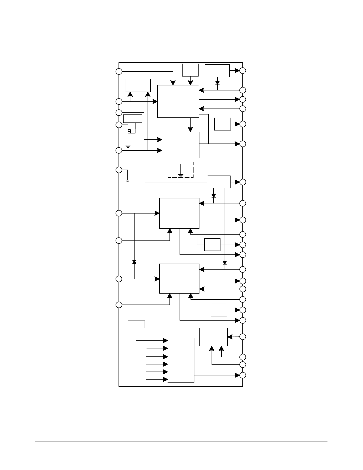
Buck Converters
Connected Switcher
(UVLO)
2.6 MHz
and are RoHS Compliant
© Semiconductor Components Industries, LLC, 2014
January , 2014 − Rev. 0
Figure 1. Evaluation Board Photo
1 Publication Order Number:
EVBUM2223/D
NCV97310MW33GEVB
STBYB
VBAT
VINL
RMIN
EN
GND1
VIN2
EN2
VDD
LOGIC
Master Enable
SEL
REGULATOR 1
3V3
STEP DOWN
LINEAR
REGULATOR
REGULATOR 2
1V2 ... 3V 3
STEP DOWN
VDRV
RSTB
VDRV VDRV2
RSTB
VDRV1
BST1
SW1
COMP1
RSTB1
VOUT
BST2
SW2
FB2
RSTB2
VIN3
EN3
REGULATOR 3
1V2...3V3
STEP DOWN
TEMP
OT
WARNING
VIN_UVLO
VIN_OV
RSTB1
RSTB2
RSTB3
ERR
Figure 2. NCV97310 Block Diagram
RSTB
OSC
GND2
BST3
SW3H
SW3L
FB3
RSTB3
GND3
ROSC
RMOD
RDEPTH
ERRB
http://onsemi.com
2
NCV97310MW33GEVB
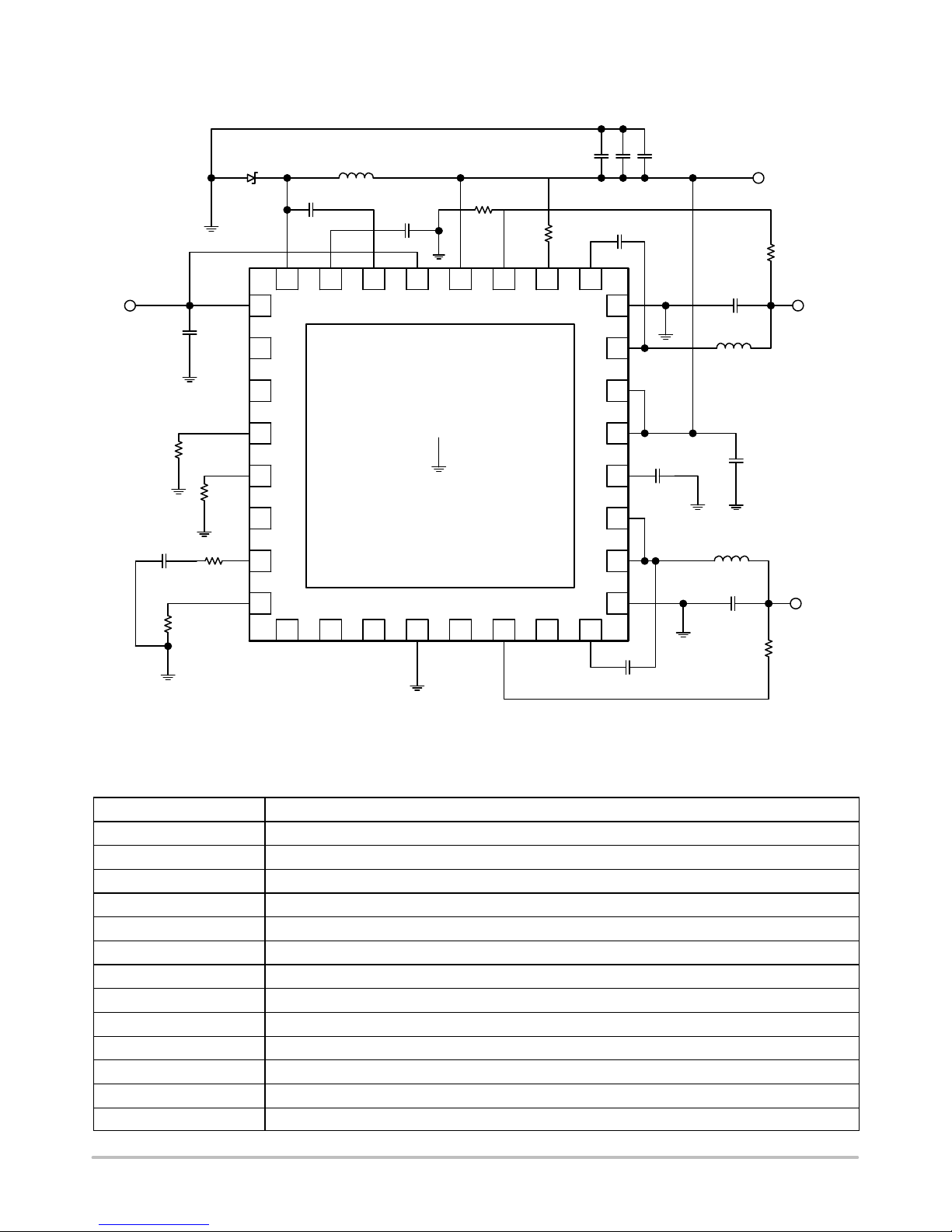
TYPICAL APPLICATION
C
OUT1
L
C
D
1
V
BAT
C
IN1
1
EN
STBYB
BST1
32 25
VBAT
1
C
DRV1
R
FB2D
R
MIN
RMINSW1 VDRV1 BST1 VINL VOUT FB2 BST2
GND2
C
24
SW2
VIN2
BST2
C
R
FB2U
OUT2
L
2
V
OUT1
V
OUT2
MOD
RDEPTH
RMOD
RSTB1
COMP1
ROSC
8
ERRB EN2 RSTB2 GND1 RSTB3 FB3 EN3 BST3
9 16
C
COMP1
R
DEPTH
R
R
COMP1
OSC
R
Table 1. EVALUATION BOARD TERMINALS
Pin Name Function
VBAT Positive dc input voltage
GND Common dc return
VOUT1 Positive 3.3 V dc output voltage (LDO/Switcher 1)
VOUT2 Positive DC output voltage (Switcher 2)
VOUT3 Positive DC output voltage (Switcher 3)
EN Master enable input. Includes jumper J3 to connect to VBAT.
STBYB Standby enable input. Includes jumper J4 to connect to VBAT.
EN2 Switcher 2 enable input. Includes jumper J6 to connect to VOUT1.
EN3 Switcher 3 enable input. Includes jumper J5 to connect to VOUT1.
ERRB
RST1B Reset with adjustable delay. Goes low when the VOUT1 is out of regulation.
RST2B Reset with adjustable delay. Goes low when the VOUT2 is out of regulation.
RST3B Reset with adjustable delay. Goes low when the VOUT3 is out of regulation.
Error flag combining temperature and input and output voltage sensing.
Figure 3. Typical Application
VIN3
VDRV2
SW3H
SW3L
GND3
17
C
BST3
C
DRV2
L
C
3
OUT3
R
FB3U
C
IN2
V
OUT3
http://onsemi.com
3
NCV97310MW33GEVB
Table 2. ABSOLUTE MAXIMUM RATINGS (Voltages are with respect to GND)
Rating
Dc Supply Voltage (VBAT, EN, STBYB) −0.3 to 36 V
Dc Supply Voltage (VIN2, VIN3) −0.3 to 12 V
Dc Supply Voltage (RSTB1, RSTB2,
RSTB3, ERRB, EN2, EN3)
Storage Temperature Range −55 to 150 °C
Stresses exceeding those listed in the Maximum Ratings table may damage the device. If any of these limits are exceeded, device functionality
should not be assumed, damage may occur and reliability may be affected.
Table 3. ELECTRICAL CHARACTERSITICS (TA = 25°C, 4.5 ≤ VIN ≤ 18 V, IOUT ≤ 2 A, unless otherwise specified)
Characteristic
REGULATION
Output Voltage (VOUT1)
Output Voltage (VOUT2) 1.8 V
Output Voltage (VOUT3) 1.2 V
Line Regulation (VOUT1) I
Line Regulation (VOUT2) I
Line Regulation (VOUT3) I
Load Regulation (VOUT1) V
Load Regulation (VOUT2) V
Load Regulation (VOUT3) V
SWITCHING
Switching Frequency
Soft-start Time 1.4 ms
R
Frequency Range
OSC
CURRENT LIMIT
Peak Current Limit (VOUT1)
Peak Current Limit (VOUT1) STBYB = 5 V 4.4 A
Peak Current Limit (VOUT2) 2.9 A
Peak Current Limit (VOUT3) 2.9 A
PROTECTION
Input Undervoltage Lockout (UVLO)
Input Overvoltage Protection V
Thermal Warning TJ Rising 150 °C
Thermal Shutdown TJ Rising 170 °C
Product parametric performance is indicated in the Electrical Characteristics for the listed test conditions, unless otherwise noted. Product
performance may not be indicated by the Electrical Characteristics if operated under different conditions.
Conditions Typical Value Unit
OUT1
OUT2
OUT3
BAT
BAT
BAT
50 kW ≥ R
STBYB = 0 V 0.2 A
V
BAT
BAT
Value Unit
−0.3 to 6 V
3.3 V
= 1.0 A 0.03 %
= 1.0 A 0.01 %
= 1.0 A 0.001 %
= 13.2 V 0.3 %
= 13.2 V 0.02 %
= 13.2 V 0.03 %
2.0 MHz
OSC
≥ 10 kW
2.0 to 2.6 MHz
Decreasing 3.9 V
Increasing 36 V
http://onsemi.com
4

(3.3 V)
VOUT1
VOUT1
NCV97310MW33GEVB
GND1
VOUT1
1
1
VOUT3
10 uF
10 uF
GND3
1
CO15
VIN2
CO14
VIN2
Place close
to VIN2
4.7 uF
Place close
to VIN2
1 uF
VOUT2
GND2
VOUT3
VOUT3
1
(1.2 V)
COUT32
COUT31
1
1
VOUT2
(1.8 V)
COUT22
10 uF
VOUT2
VIN2
COUT21
R7
0.0
10 uF
SW1
COUT13
10 uF
COUT12
10 uF
0.1 uF
DRV1
VIND
10K
BST2
0.1 uF
C3
VBAT_IC
CIN4
CIN3
CIN2
CIN1
CBST2
33
25
26
27
28
29
30
31
32
U1
J2
J1
2.2 uF
1 uF
4.7 uF
4.7 uF
COUT11
10 uF
L1
4.7 uH
SW1
D1
NRVB440MFS
C1
RFB2L
20.0K
R1
CBST1
100 pF
0.0
FB2
50V
0.1 uF
RFB2U
FB2
CDRV1
CSNB2
100 pF
L2 2.2 uH
RSNB2
10.0
SW2
0.1 uF
EPAD
BST2
NC
FB2
VINL
BST1
SW1
1 2
1 2
24
VOUT
VDRV1
VIN2
SW2
23
22
SW2
EN
EN
STBYB
STBYB
VIN321VIN2
TP1
RDEPTH
DNP
VOUT1
NCV97310MW33R2G
TP2
GND2
VBAT1EN2STBY3RDEPTH4RMOD5RST16COMP17ROSC
CDRV2
0.47 uF
20
VDRV2
RMOD
DNP
SW3
19
SW3H
RST1B
R3
SW3
18
COMP1
10K
L3 1.0 uH
SW3L
COMP1
CSNB3
RSNB3
17
GND3
8
ROSC
RCOMP1
100 pF
10.0
TP3
12.4K
CBST3
0.1 uF
BST3
EN3
FB3
RST3
GND1
RST2
EN2
ERR
9
ROSC
CCOMP2
VOUT1
VOUT1
J3
EN3
BST3
16
15
14
13
12
11
10
GND
DNP
CCOMP1
22 pF
1 2
EN3
FB3
Place GND near
330 pF
R4
10K
C2
10K
RFB3U
R2
FB3
RFB3L
DNP
ERRB for logic
reference.
VOUT1
ERRB
ERRB
R5
10K
VOUT1
VOUT1
100 pF
0.0
EN2
J4
1 2
R6
10K
EN2
RST2B
RST2B
RST3B
RST3B
Figure 4. NCV97310GEVB 3.3 V Board Schematic
Place CIN0, L0, CIN1, CIN2 on VBAT side.
Place CIN3 close to VINL (pin 29)
CIN5
Place CIN4 close to VBAT (pin 1)
L0
1.0 uH
CIN0
VBAT
VBAT_1
1
100 uF
4.7 uF
VBAT
Place CIN5 on
bottom of PCB
1
GND0
http://onsemi.com
5
RST1B
 Loading...