

Page 1
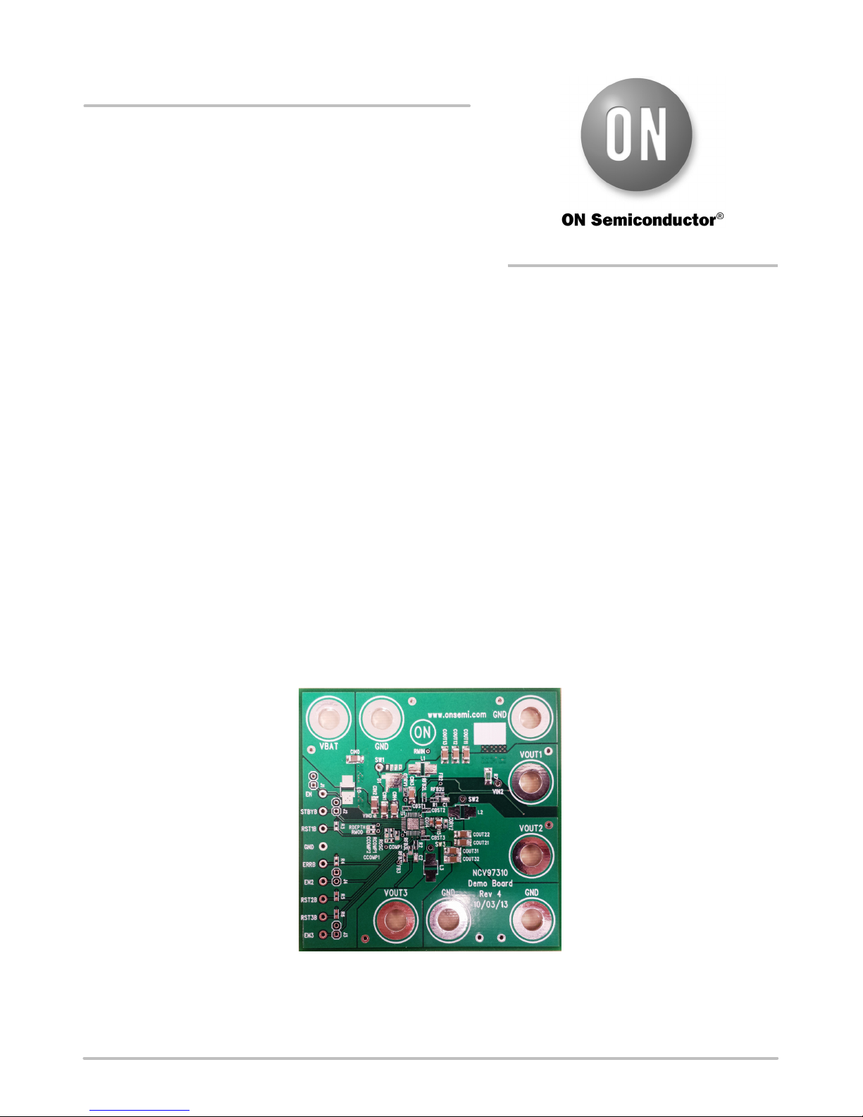
NCV97310MW50GEVB
NCV97310 Evaluation Board
User'sManual
Description
The NCV97310 is 3−output regulator consisting of
a low−Iq battery−connected 3 A 2 MHz non−synchronous
switcher and two low−voltage 1.5 A 2 MHz synchronous
switchers; all using integrated power transistors.
The high−voltage switcher is capable of converting
a 4.1 V to 18 V battery input to a 5 V or 3.3 V output at
a constant 2MHz switching frequency, delivering up to 3A.
In overvoltage conditions up to 36 V, the switching
frequency folds back to 1 MHz; in load dump conditions up
to 45 V the regulator shuts down.
The output of the battery− connected buck r egulator serves
as the l ow v oltage i nput f or t he 2 s ynchronous s witchers. E ach
downstream output is adjustable from 1.2 V to 3.3 V, with
a 1.5 A current limit and a constant 2 MHz switching
frequency. Each switcher has independent enable and reset
pins, giving extra power management flexibility.
For low−Iq operating mode the low−voltage switchers are
disabled, and the standby rail is supplied by a low−Iq LDO
(up to 150 mA) with a typical Iq of 30 mA. The LDO
regulator is in parallel to the high−voltage switcher, and is
activated when the switcher is forced in standby mode.
All 3 SMPS outputs use peak current mode control with
internal slope compensation, internally−set soft−start,
battery undervoltage lockout, battery overvoltage
protection, cycle−by−cycle current limiting, hiccup mode
short−circuit protection and thermal shutdown. An error flag
is available for diagnostics.
Key Features
• Low Quiescent Current in Standby Mode
• 2 Microcontroller Enabled Low Voltage Synchronous
• Large Conversion Ratio of 18 V to 3.3 V Battery
• Wide Input of 4.1 to 45 V with Undervoltage Lockout
• Fixed Frequency Operation Adjustable from 2.0 to
• Internal 1.5 ms Soft−starts
• Cycle−by−cycle Current Limit Protections
• Hiccup Overcurrent Protections (OCP)
• Individual Reset Pins with Adjustable Delays
• These Devices are Pb−Free, Halogen Free/BFR Free
Typical Applications
• Infotainment, Body Electronics, Telematics, ECU
http://onsemi.com
EVAL BOARD USER’S MANUAL
Buck Converters
Connected Switcher
(UVLO)
2.6 MHz
and are RoHS Compliant
© Semiconductor Components Industries, LLC, 2014
October, 2014 − Rev. 1
Figure 1. Evaluation Board Photo
1 Publication Order Number:
EVBUM2218/D
Page 2
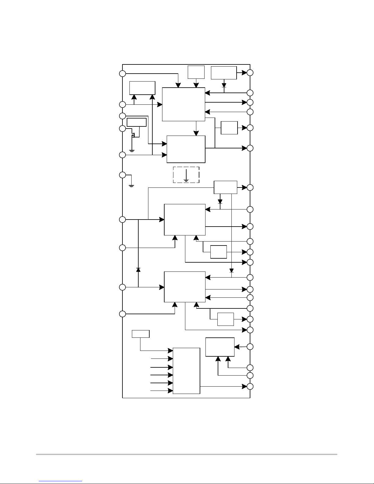
NCV97310MW50GEVB
STBYB
VBAT
VINL
RMIN
EN
GND1
VIN2
EN2
VDD
LOGIC
Master Enable
SEL
REGULATOR 1
5V or 3V3
STEP DOWN
LINEAR
REGULATOR
REGULATOR 2
1V2 ... 3V3
STEP DOWN
VDRV
RSTB
VDRV VDRV2
RSTB
VDRV1
BST1
SW1
COMP1
RSTB1
VOUT
BST2
SW2
FB2
RSTB2
VIN3
EN3
REGULATOR 3
1V2...3V3
STEP DOWN
TEMP
OT
WARNING
VIN_UVLO
VIN_OV
RSTB1
RSTB2
RSTB3
ERR
Figure 2. NCV97310 Block Diagram
RSTB
OSC
GND2
BST3
SW3H
SW3L
FB3
RSTB3
GND3
ROSC
RMOD
RDEPTH
ERRB
http://onsemi.com
2
Page 3
NCV97310MW50GEVB
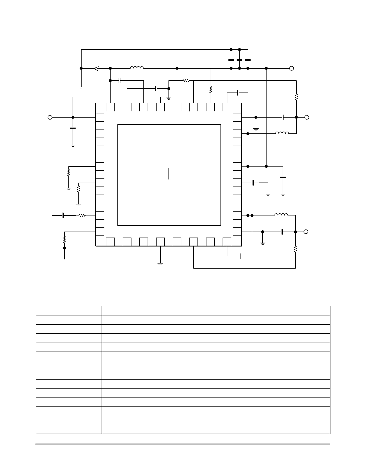
TYPICAL APPLICATION
C
OUT1
L
C
D
1
V
BAT
C
IN1
1
EN
STBYB
BST1
32 25
VBAT
1
C
DRV1
R
FB2D
R
MIN
RMINSW1 VDRV1 BST1 VINL VOUT FB2 BST2
GND2
C
24
SW2
VIN2
BST2
C
R
FB2U
OUT2
L
2
V
OUT1
V
OUT2
MOD
RDEPTH
RMOD
RSTB1
COMP1
ROSC
8
ERRB EN2 RSTB2 GND1 RSTB3 FB3 EN3 BST3
9 16
C
COMP1
R
DEPTH
R
R
COMP1
OSC
R
Table 1. EVALUATION BOARD TERMINALS
Pin Name Function
VBAT Positive dc input voltage
GND Common dc return
VOUT1 Positive 5.0 V dc output voltage (LDO / switcher 1)
VOUT2 Positive DC output voltage (switcher 2)
VOUT3 Positive DC output voltage (switcher 3)
EN Master enable input. Includes jumper J3 to connect to VBAT.
STBYB Standby enable input. Includes jumper J4 to connect to VBAT.
EN2 Switcher 2 enable input. Includes jumper J6 to connect to VOUT1.
EN3 Switcher 3 enable input. Includes jumper J5 to connect to VOUT1.
ERRB
RST1B Reset with adjustable delay. Goes low when the VOUT1 is out of regulation.
RST2B Reset with adjustable delay. Goes low when the VOUT2 is out of regulation.
RST3B Reset with adjustable delay. Goes low when the VOUT3 is out of regulation.
Error flag combining temperature and input and output voltage sensing.
Figure 3. Typical Application
VIN3
VDRV2
SW3H
SW3L
GND3
17
C
BST3
C
DRV2
L
C
3
OUT3
R
FB3U
C
IN2
V
OUT3
http://onsemi.com
3
Page 4

NCV97310MW50GEVB
Table 2. ABSOLUTE MAXIMUM RATINGS (Voltages are with respect to GND)
Rating
Dc Supply Voltage (VBAT, EN, STBYB) −0.3 to 36 V
Dc Supply Voltage (VIN2, VIN3) −0.3 to 12 V
Dc Supply Voltage (RSTB1, RSTB2,
RSTB3, ERRB, EN2, EN3)
Storage Temperature Range −55 to 150 °C
Stresses exceeding those listed in the Maximum Ratings table may damage the device. If any of these limits are exceeded, device functionality
should not be assumed, damage may occur and reliability may be affected.
Value Unit
−0.3 to 6 V
Table 3. ELECTRICAL CHARACTERSITICS (T
Characteristic
= 25°C, 4.5 ≤ VIN ≤ 18 V, IOUT ≤ 2 A, unless otherwise specified)
A
Conditions Typical Value Unit
REGULATION
Output Voltage (VOUT1)
5.0 V
Output Voltage (VOUT2) 3.3 V
Output Voltage (VOUT3) 1.2 V
Line Regulation (VOUT1) I
Line Regulation (VOUT2) I
Line Regulation (VOUT3) I
Load Regulation (VOUT1) V
Load Regulation (VOUT2) V
Load Regulation (VOUT3) V
= 1.0 A 0.03 %
OUT1
= 1.0 A 0.01 %
OUT2
= 1.0 A 0.001 %
OUT3
= 13.2 V 0.3 %
BAT
= 13.2 V 0.02 %
BAT
= 13.2 V 0.03 %
BAT
SWITCHING
Switching Frequency
2.0 MHz
Soft−start Time 1.4 ms
R
Frequency Range
OSC
50 kW ≥ R
OSC
≥ 10 kW
2.0 to 2.6 MHz
CURRENT LIMIT
Peak Current Limit (VOUT1)
STBYB = 0 V 0.2 A
Peak Current Limit (VOUT1) STBYB = 5 V 4.4 A
Peak Current Limit (VOUT2) 2.9 A
Peak Current Limit (VOUT3) 2.9 A
PROTECTION
V
Input Undervoltage Lockout (UVLO)
Input Overvoltage Protection V
Decreasing 3.9 V
BAT
Increasing 36 V
BAT
Thermal Warning TJ Rising 150 °C
Thermal Shutdown TJ Rising 170 °C
Product parametric performance is indicated in the Electrical Characteristics for the listed test conditions, unless otherwise noted. Product
performance may not be indicated by the Electrical Characteristics if operated under different conditions.
http://onsemi.com
4
Page 5
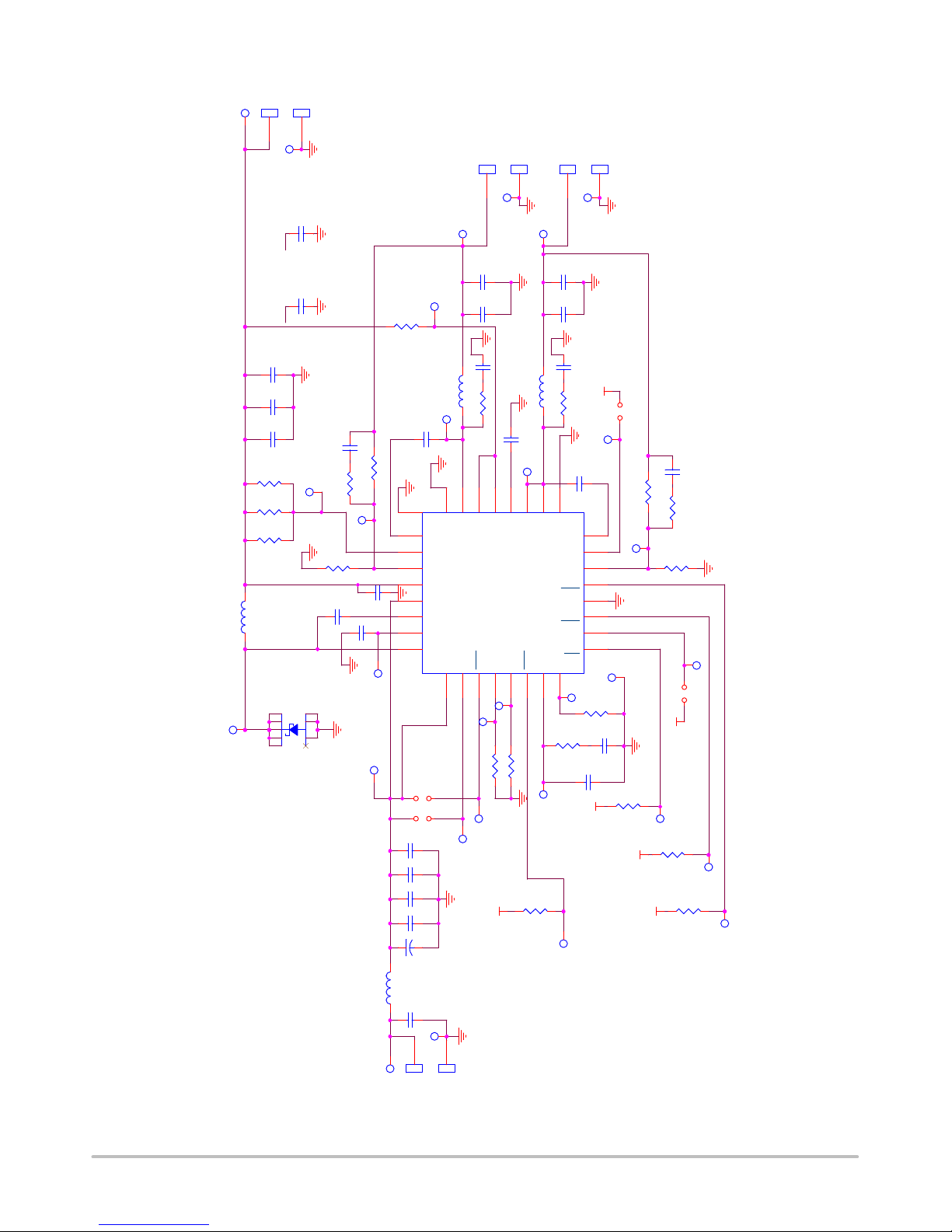
VOUT1
VOUT1
(5.0 V)
1
VOUT1
CO15
VIN2
CO14
VIN2
GND1
1
Place close
to VIN2
4.7 uF
Place close
to VIN2
1 uF
NCV97310MW50GEVB
VOUT2
GND2
VOUT3
VOUT3
1
(1.2 V)
COUT32
COUT31
1
1
VOUT2
(3.3 V)
COUT22
10 uF
VOUT2
VIN2
COUT21
R7
0.0
10 uF
10 uF
10 uF
VOUT3
GND3
1
SW1
COUT13
10 uF
COUT12
10 uF
0.1 uF
DRV1
VIND
10K
BST2
0.1 uF
C3
VBAT_IC
CIN4
CIN3
CIN2
CIN1
CBST2
33
25
26
27
28
29
30
31
32
U1
J2
J1
2.2 uF
1 uF
4.7 uF
4.7 uF
COUT11
10 uF
100
RMIN3
100
RMIN2
100
RMIN1
L1
4.7 uH
SW1
D1
RMIN
NRVB440MFS
C1
RFB2L
5.76K
R1
RMIN
CBST1
100 pF
0.0
FB2
50V
0.1 uF
RFB2U
FB2
CDRV1
CSNB2
100 pF
L2 2.2 uH
RSNB2
10.0
SW2
0.1 uF
FB2
1 2
1 2
24
BST2
RMIN
VINL
BST1
SW1
EPAD
VOUT
VIN2
SW2
23
22
SW2
EN
EN
STBYB
STBYB
VIN321VIN2
TP1
RDEPTH
DNP
VOUT1
NCV97310MW50R2G
TP2
GND2
VDRV1
VBAT1EN2STBY3RDEPTH4RMOD5RST16COMP17ROSC
CDRV2
0.47 uF
20
VDRV2
RMOD
DNP
SW3
19
SW3H
RST1B
R3
SW3
18
SW3L
COMP1
10K
CSNB3
L3 1.0 uH
RSNB3
17
8
ROSC
COMP1
100 pF
10.0
GND3
TP3
RCOMP1
12.4K
CBST3
0.1 uF
BST3
EN3
FB3
RST3
GND1
RST2
EN2
ERR
9
ROSC
CCOMP2
VOUT1
VOUT1
J3
EN3
BST3
16
15
14
13
12
11
10
GND
DNP
CCOMP1
22 pF
1 2
EN3
FB3
Place GND near
330 pF
R4
10K
C2
10K
RFB3U
R2
FB3
RFB3L
DNP
ERRB for logic
reference.
VOUT1
ERRB
ERRB
R5
10K
VOUT1
VOUT1
100 pF
0.0
EN2
J4
1 2
R6
10K
EN2
RST2B
RST2B
RST3B
RST3B
Figure 4. NCV97310GEVB 5.0 V Board Schematic
Place CIN0, L0, CIN1, CIN2 on VBAT side.
Place CIN3 close to VINL (pin 29)
CIN5
Place CIN4 close to VBAT (pin 1)
L0
1.0 uH
CIN0
VBAT
VBAT_1
1
100 uF
4.7 uF
VBAT
Place CIN5 on
bottom of PCB
1
GND0
http://onsemi.com
5
RST1B
Page 6

Operational Guidelines
1. Connect a dc input voltage, within the 6.0 V to 36
V range, between VBAT and GND.
2. Connect a load (< 150 mA) between VOUT1 and
GND
3. Connect a dc enable voltage, within the 2.0 V to
36 V range, between EN and GND. This will
enable the internal LDO for low Iq mode. You
may use jumper J1 to connect EN directly to
VBAT.
a. The VOUT1 signal should be 5.0 V.
b. The VOUT2 signal should be disabled
(regardless of EN2 state) and read 0 V.
c. The VOUT3 signal should be disabled
(regardless of EN3 state) and read 0 V.
4. Connect a dc enable voltage, within the 2.0 V to
36 V range, between STBYB and GND. This will
exit low Iq mode and power up switcher 1. You
may use jumper J2 to connect STBYB directly to
VBAT.
The VOUT1 signal should still be 5.0 V. You
may now add a higher load to VOUT1.
NCV97310MW50GEVB
5. Connect a dc enable voltage, within the 2.0 V to
6 V range, between EN2 and GND. This will
power up switcher 2. You may use jumper J4 to
connect EN2 directly to VOUT1.
The VOUT2 signal should be 3.3 V.
6. Connect a dc enable voltage, within the 2.0 V to
6 V range, between EN3 and GND. This will
power up switcher 3. You may use jumper J3 to
connect EN3 directly to VOUT1.
The VOUT3 signal should be 1.2 V.
Figure 5. NCV97310 Board Connections
http://onsemi.com
6
Page 7

NCV97310MW50GEVB
APPLICATION INFORMATION
Output Voltage Selection
The voltage outputs for switcher 2 and switcher 3 are
adjustable and can be set with a resistor divider. The FB
reference for both switchers is 1.2 V.
VOUT 2 (VOUT 3)
Time Domain Frequency Domain
Unmodulated
V
R
UPPER
FBx = 1 .2 V
R
LOWER
The upper resistor is set to 10 kW and is part of the
feedback loop. To maintain stability over all conditions, it is
recommended to change the only the lower feedback resistor
to set the output voltage. Use the following equation:
V
R
LOWER
+ R
UPPER
FB
V
*V
FB
OUT
Some common setups are listed below:
Desired
Output (V)
1.2 1.2 10.0 NP
1.5 1.2 10.0 40.0
1.8 1.2 10.0 20.0
2.5 1.2 10.0 9.31
3.3 1.2 10.0 5.76
VREF (V)
R
UPPER
(kW, 1%)
R
LOWER
(kW, 1%)
t
V
t
f
c
f
c
9f
c7fc5fc3fc
9f
c7fc5fc3fc
The spread spectrum used in the NCV97310 is an
“up−spread” technique, meaning the switching frequency is
spread upward from the 2.0 MHz base frequency. For
example, a 5 % spread means that the switching frequency
is swept (spread) from 2.0 MHz up to 2.1 MHz in a linear
fashion – this is called the modulation depth. The rate at
which this spread takes place is called the modulation
frequency. For example, a 10 kHz modulation frequency
means that the frequency is swept from 2.0 MHz to 2.1 MHz
in 50 ms and then back down from 2.1 MHz to 2.0 MHz in
50 ms.
Spread Spectrum
In SMPS devices, switching translates to higher
efficiency. Unfortunately, the switching leads to a much
noisier EMI profile. We can greatly decrease some of the
radiated emissions with some spread spectrum techniques.
Spread spectrum is used to reduce the peak electromagnetic
emissions of a switching regulator.
http://onsemi.com
7
Page 8

NCV97310MW50GEVB
The modulation depth and modulation frequency are each
set by 2 external resistors to GND. The modulation
frequency can be set from 5 kHz up to 50 kHz using a resistor
from the RMOD pin to GND. The modulation depth can be
set from 3% up to 30% of the nominal switching frequency
using a resistor from the RDEPTH pin to GND. Please see
the curves below for typical values:
Spread spectrum i s a u t o m a t i c a l l y t u r n e d o ff when there is
a short to GND or an open circuit on either the RMOD pin
or the RDEPTH pin. Please be sure that the ROSC pin is an
open circuit when using spread spectrum.
Efficiency
0.9
0.8
0.7
0.6
0.5
0.4
0.3
0.2
TYPICAL PERFORMANCE
NCV97310 − SW1 Efficiency − 5.0 V
1
VIN = 8.0 V
VIN = 13.2 V
VIN = 18.0 V
0.1
0
0 0.5 1 1.5 2 2.5 3 3.5
Figure 6. Efficiency for SW1 with a 5.0 V Output
http://onsemi.com
8
Page 9

NCV97310MW50GEVB
NCV97310 − SW2 Efficiency − 3.3 V
100%
90%
80%
70%
60%
50%
Efficiency
40%
30%
20%
10%
0%
0 0.5 1 1.5 2 2.5
Output Current (A)
VIN = 5.0 V
VIN = 8.0 V
100%
90%
80%
70%
60%
50%
40%
Efficiency
30%
20%
10%
Figure 7. Efficiency for SW2 with a 3.3 V Output
NCV97310 − SW3 Efficiency − 1.2 V
VIN = 3.3 V
VIN = 5.0 V
0%
0 0.5 1 1.5 2 2.5
Figure 8. Efficiency for SW3 with a 1.2 V Output
Output Current (A)
http://onsemi.com
9
Page 10

Line Regulation
2.00%
1.50%
1.00%
0.50%
NCV97310MW50GEVB
NCV97310 − SW1 − 3.3 V − Line Regulation
0.00%
0 5 10 15 20 25 30
−0.50%
Line Regulation
−1.00%
−1.50%
−2.00%
0.10%
0.05%
IOUT = 100 mA
IOUT = 500 mA
IOUT = 1.0 A
IOUT = 2.0 A
IOUT = 3.0 A
Input Voltage (V)
Figure 9. Line Regulation for SW1 with a 3.3 V Output
NCV97310 − SW2 − 3.3 V − Line Regulation
0.00%
3456789
Line Regulation
−0.05%
−0.10%
Figure 10. Line Regulation for SW2 with a 3.3 V Output
IOUT = 100 mA
IOUT = 500 mA
IOUT = 1.0 A
IOUT = 2.0 A
Input Voltage (V)
http://onsemi.com
10
Page 11

0.10%
0.05%
NCV97310MW50GEVB
NCV97310 − SW3 − 1.2 V − Line Regulation
0.00%
3 3.5 4 4.5 5 5.5
Line Regulation
−0.05%
−0.10%
Load Regulation
0.40%
0.30%
0.20%
IOUT = 100 mA
IOUT = 500 mA
IOUT = 1.0 A
IOUT = 2.0 A
Input Voltage (V)
Figure 11. Line Regulation for SW3 with a 1.2 V Output
NCV97310 − SW1 Load Regulation − 5.0 V
0.10%
0.00%
Load Regulation
−0.10%
−0.20%
−0.30%
−0.40%
0 0.5 1 1.5 2 2.5 3 3.5
Figure 12. Load Regulation for SW1 with a 5.0 V Output
VIN = 8.0 V
VIN = 13.2 V
VIN = 18.0 V
Output Current (A)
http://onsemi.com
11
Page 12

0.10%
0.05%
0.00%
NCV97310MW50GEVB
NCV97310 − SW2 Load Regulation − 3.3 V
Load Regulation
−0.05%
−0.10%
0 0.5 1 1.5 2 2.5
0.10%
0.05%
VIN = 5.0 V
VIN = 8.0 V
Output Current (A)
Figure 13. Load Regulation for SW2 with a 3.3 V Output
NCV97310 − SW3 Load Regulation − 1.2 V
0.00%
Load Regulation
−0.05%
−0.10%
0 0.5 1 1.5 2 2.5
Figure 14. Load Regulation for SW3 with a 1.2 V Output
VIN = 3.3 V
VIN = 5.0 V
Output Current (A)
http://onsemi.com
12
Page 13

VOUT1
VOUT1
(5.0 V)
1
VOUT1
CO15
VIN2
CO14
VIN2
GND1
1
Place close
to VIN2
4.7 uF
Place close
to VIN2
1 uF
NCV97310MW50GEVB
SCHEMATIC
VOUT2
GND2
1
VOUT2
(3.3 V)
COUT22
10 uF
VOUT2
VIN2
COUT21
R7
0.0
10 uF
1
1
VOUT3
(1.2 V)
COUT32
VOUT3
COUT31
10 uF
10 uF
VOUT3
GND3
1
SW1
COUT13
10 uF
COUT12
10 uF
0.1 uF
DRV1
VIND
10K
BST2
C3
VBAT_IC
0.1 uF
CIN4
CIN3
CIN2
CIN1
CBST2
33
25
26
27
28
29
30
31
32
U1
J2
J1
2.2 uF
1 uF
4.7 uF
4.7 uF
COUT11
10 uF
100
RMIN3
100
RMIN2
100
RMIN1
L1
4.7 uH
SW1
D1
RMIN
NRVB440MFS
C1
RFB2L
5.76K
R1
RMIN
CBST1
100 pF
0.0
FB2
50V
0.1 uF
RFB2U
FB2
CDRV1
CSNB2
100 pF
L2 2.2 uH
RSNB2
10.0
SW2
0.1 uF
24
BST2
RMIN
FB2
VINL
BST1
SW1
1 2
1 2
VIN2
SW2
22
23
EPAD
SW2
EN
EN
STBYB
STBYB
VIN321VIN2
TP1
RDEPTH
DNP
VOUT1
NCV97310MW50R2G
TP2
GND2
VOUT
VDRV1
VBAT1EN2STBY3RDEPTH4RMOD5RST16COMP17ROSC
CDRV2
0.47 uF
20
VDRV2
RMOD
DNP
SW3
19
SW3H
RST1B
R3
SW3
18
COMP1
10K
CSNB3
L3 1.0 uH
17
SW3L
8
ROSC
COMP1
RSNB3
GND3
TP3
RCOMP1
100 pF
10.0
CBST3
BST3
EN3
FB3
RST3
GND1
RST2
EN2
ERR
12.4K
CCOMP2
0.1 uF
16
15
14
13
12
11
10
9
ROSC
DNP
CCOMP1
22 pF
VOUT1
VOUT1
J3
EN3
BST3
GND
1 2
EN3
FB3
Place GND near
330 pF
R4
10K
C2
10K
RFB3U
R2
FB3
RFB3L
ERRB for logic
reference.
VOUT1
ERRB
ERRB
R5
10K
VOUT1
VOUT1
0.0
DNP
100 pF
EN2
J4
1 2
R6
10K
EN2
RST2B
RST2B
RST3B
RST3B
Place CIN0, L0, CIN1, CIN2 on VBAT side.
Place CIN3 close to VINL (pin 29)
CIN5
Place CIN4 close to VBAT (pin 1)
L0
1.0 uH
CIN0
VBAT
VBAT_1
100 uF
4.7 uF
1
VBAT
Place CIN5 on
bottom of PCB
1
GND0
http://onsemi.com
13
RST1B
Page 14

NCV97310MW50GEVB
PCB LAYOUT
Figure 15. Top View
Figure 16. Bottom View
http://onsemi.com
14
Page 15

Table 4. BILL OF MATERIALS
Reference
Designator(s)
C1, C2, CSNB2,
CSNB3
C3, CBST1,
CBST2, CBST3,
CDRV1
CCOMP1 1 CAP CER
CCOMP2 1 CAP CER
CDRV2 1 CAP CER
CIN0, CIN1,
CIN2
CIN3 1 CAP CER
CIN4 1 CAP CER
CIN5 1 CAP ALUM
CO14 1
CO15 1 CAP CER
COUT11,
COUT12,
COUT13,
COUT21,
COUT22,
COUT31,
COUT32
R1, R2 2 RES 0.0 OHM
R3, R4, R5, R6,
RFB2U, RFB3U
R7 1 RES 0.0 OHM
RCOMP1 1 RES 12.4K
RFB2L 1 RES 20.0K
RMIN1, RMIN2,
RMIN3
RSNB2, RSNB3 2 RES 10.0 OHM
D1 1 DIODE
Qty. Description Value Tolerance Footprint Manufacturer
4 CAP CER
100 pF 50 V 5%
NP0 0603
5 CAP CER
0.1 mF 50 V
10% X7R 0603
330 pF 50 V 5%
NP0 0603
22 pF 50 V 5%
NP0 0603
0.47 mF 16 V
10% X7R 0603
3 CAP CER
4.7 mF 50 V
10% X7R 1206
1.0 mF 50 V
10% X7R 1206
2.2 mF 50 V
10% X7R 1206
100 mF 50 V
20% SMD
CAP CER 1 mF
16 V 10% X7R
0603
4.7 mF 16 V
10% X7R 0805
7 CAP CER
10 mF 10 V 10%
X7R 1206
1/10 W 0603
SMD
6 RES 10.0K
OHM 1/10 W
1% 0603 SMD
1/4 W 1206
SMD
OHM 1/10 W
1% 0603 SMD
OHM 1/10 W
1% 0603 SMD
3 RES 100 OHM
1/4 W 1% 1206
SMD
1/10 W 1%
0603 SMD
SCHOTTKY
4.0 A 40 V SMB
NCV97310MW50GEVB
BILL OF MATERIALS
Manufacturer’s
Part Number
100 pF 5% 603 Murata Electronics
0.1 mF
330 pF 5% 603 Murata Electronics
22 pF 5% 603 Murata Electronics
0.47 mF
4.7 mF
1.0 mF
2.2 mF
100 mF
1.0 mF
4.7 mF
10 mF
0 W
10.0 kW
0 W
12.4 kW
20.0 kW
100 W
10.0 W
40 V/4.0 A N/A SMB_DIODE ON Semiconductor NRVB440MFST1G No
10% 603 Murata Electronics
10% 603 Murata Electronics
10% 1206 TDK Corporation C3216X7R1H475K160AC Yes
10% 1206 Murata Electronics
10% 1206 Murata Electronics
20% FK_V_E Chemi-Con EMZA500ADA101MHA0G Yes
10% 603 Murata Electronics
10% 805 TDK Corporation CGA4J3X7R1C475K125AB Yes
10% 1206 Murata Electronics
Jumper 603 Vishay/Dale CRCW06030000Z0EA Yes
1% 603 Vishay/Dale CRCW060310K0FKEA Yes
Jumper 1206 Vishay/Dale CRCW12060000Z0EA Yes
1% 603 Vishay/Dale CRCW060312K4FKEA Yes
1% 603 Vishay/Dale CRCW060320K0FKEA Yes
1% 1206 Vishay/Dale CRCW1206100RFKEA Yes
1% 603 Vishay/Dale CRCW060310R0FKEA Yes
North America
North America
North America
North America
North America
North America
North America
North America
North America
GCM1885C1H101JA16D Yes
GCM188R71H104KA57D Yes
GCM1885C1H331JA16D Yes
GCM1885C1H220JA16D Yes
GCM188R71C474KA55D Yes
GCM31MR71H105KA55L Yes
GCM31CR71H225KA55L Yes
GCM188R71C105KA64D Yes
GCM31CR71A106KA64L Yes
Substi-
tution
Allowed
http://onsemi.com
15
Page 16

Table 4. BILL OF MATERIALS (continued)
P
al
Reference
Designator(s)
L0, L3 2 High Current
L1 1 High Current
L2 1 High Current
EN, EN2, EN3,
ERRB, GNDL,
PGND1_1,
PGND1_2,
PGND2_1,
PGND3_1,
RST1B, RST2B,
RST3B, STBYB,
SW1, SW2,
SW3, VIN2,
VBAT,
VOUT1_1,
VOUT2_1,
VOUT3_1
GND0, GND1,
GND2, GND3,
VBAT, VOUT1,
VOUT2, VOUT3
J1, J2, J3, J4
COMP1, DRV1,
FB2, FB3,
RMIN, TP1,
TP2, TP3, VIND
RDEPTH,
RFB3L, RMOD,
ROSC
U1 1 Automotive
21 PIN INBOARD
8 CONN JACK
4 CONN
4 CONN
9 CIRCUIT PIN
4 Do Not
Shielded
Inductor 1.0 mH,
8.7 A SAT
Shielded
Inductor 4.7 mH,
4.5 A SAT
Shielded
Inductor 2.2 mH,
5.6 A SAT
.042″ HOLE
1000/PKG
BANANA
UNINS PANEL
MOU
HEADER 2POS
.100 VERT
GOLD
JUMPER
SHORTING
GOLD
PRNTD .020″D
.425″L
Battery-Connec
ted Low IQ
Multi-Output
PMU
NOTE: All devices are RoHS Compliant.
1.0 mH
4.7 mH
2.2 mH
Do Not
Populate
Populate
NCV97310MW50GEVB
ManufacturerFootprintToleranceValueDescriptionQty.
20% XAL4020-102ME Coilcraft XAL4020-102ME No
20% XAL4030-472ME Coilcraft XAL4030-472ME No
20% XAL4020-222ME Coilcraft XAL4020-222ME No
N/A N/A TP Vector Electronics K24C/M Yes
N/A N/A BANANA Emerson Network
N/A N/A JMP Molex Connector
N/A N/A JMP Sullins Connector
N/A SMALLTP Mill-Max
603 Yes
N/A N/A QFN32 ON Semiconductor NCV97310MW50R2G No
Power Connectivity
Johnson
Corporation
Solutions
Manufacturing
Corp.
Manufacturer’s
Part Number
108-0740-001 No
22-28-4023 Yes
SSC02SYAN Yes
3128-2-00-15-00-00-08-0 Yes
Substi-
tution
Allowed
ON Semiconductor and the are registered trademarks of Semiconductor Components Industries, LLC (SCILLC) or its subsidiaries in the United States and/or other countries.
SCILLC owns the rights to a number of patents, trademarks, copyrights, trade secrets, and other intellectual property. A listing of SCILLC’s product/patent coverage may be accessed
at www.onsemi.com/site/pdf/ Patent− Marking.pdf . S CILLC reserves t he right to m ake changes wit hout further notice to any products h erein. SCILLC makes no warranty, representation
or guarantee regarding the suitability of its products for any particular purpose, nor does SCILLC assume any liability arising out of the application or use of any product or circuit, and
specifically disclaims any and all liability, including without limitation special, consequential or incidental damages. “Typical” parameters which may be provided in SCILLC data sheets
and/or specifications can and do vary in different applications and actual performance may vary over time. All operating parameters, including “Typicals” must be validated for each
customer application by customer’s technical e xperts. SCILLC does not convey any license u nder its patent rights nor the rights of others. SCILLC p roducts a re n ot d esigned, i ntended,
or authorized for use as components in systems intended for surgic al i mplant into the body, or other applications intended t o s upport o r s ust ain life, or for any other application in which
the failure of the SCILLC product could create a situation where personal injury or death may occur. Should Buyer purchase or use SCILLC products for any such unintended or
unauthorized application, Buyer shall indemnify and hold SCILLC and its officers, em ployees, subsidiaries, affiliates, and distributors harmless against all claims, costs, damages, and
expenses, and reasonable at torney f ees a r ising o ut o f, d irectly o r indirectly, any claim o f personal injury or death associated w ith s uch u nintended o r u nauthorized u se, e ven if such claim
alleges that SCILLC was negligent r egarding the design o r manuf acture o f t he p art. SCILLC is a n E qual O pportunity/Af firmative Ac tion Employer. This literature is subject to all a pplicable
copyright laws and is not for resale in any manner.
UBLICATION ORDERING INFORMATION
LITERATURE FULFILLMENT:
Literature Distribution Center for ON Semiconductor
P.O. Box 5163, Denver, Colorado 80217 USA
Phone: 303−675−2175 or 800−344−3860 Toll Free USA/Canada
Fax: 303−675−2176 or 800−344−3867 Toll Free USA/Canada
Email: orderlit@onsemi.com
N. American Technical Support: 800−282−9855 Toll Free
USA/Canada
Europe, Middle East and Africa Technical Support:
Phone: 421 33 790 2910
Japan Customer Focus Center
Phone: 81−3−5817−1050
http://onsemi.com
16
ON Semiconductor Website: www.onsemi.com
Order Literature: http://www.onsemi.com/orderlit
For additional information, please contact your loc
Sales Representative
EVBUM2218/D
 Loading...