

Page 1
NCV891330
Step-Down Regulator Automotive, Low-Iq,
Dual-Mode
3 A, 2 MHz
The NCV891330 is a Dual Mode regulator intended for Automotive,
battery−connected applications that must operate with up to a 45 V
input supply. Depending on the output load, it operates either as a PWM
Buck Converter or as a Low Drop−Out Linear Regulator, and is suitable
for systems with low noise and Low Quiescent Current requirements
often encountered in automotive driver information systems. A reset
pin (with fixed delay) simplifies interfacing with a microcontroller.
The NCV891330 also provides several protection features expected
in automotive power supply systems such as current limit, short circuit
protection, and thermal shutdown. In addition, the high switching
frequency produces low output voltage ripple even when using small
inductor values and an all−ceramic output filter capacitor – forming a
space−efficient switching regulator solution.
Features
• 30 mA Iq in Light Load Condition
• 3.0 A Maximum Output Current in PWM Mode
• Internal N−channel Power Switch
• V
Operating Range 3.7 V to 36 V
IN
• Withstands Load Dump to 45 V
• Logic Level Enable Pin can be Tied to Battery
• Fixed Output Voltage of 5.0 V, 4.0 V, 3.8 V or 3.3 V
• 2 MHz Free−running Switching Frequency
• ±2 % Output Voltage Accuracy
• NCV Prefix for Automotive Requiring Site and Control Changes
• These Devices are Pb−Free and are RoHS Compliant
Typical Applications
• Audio
• Infotainment
• Instrumentation
• Safety−Vision Systems
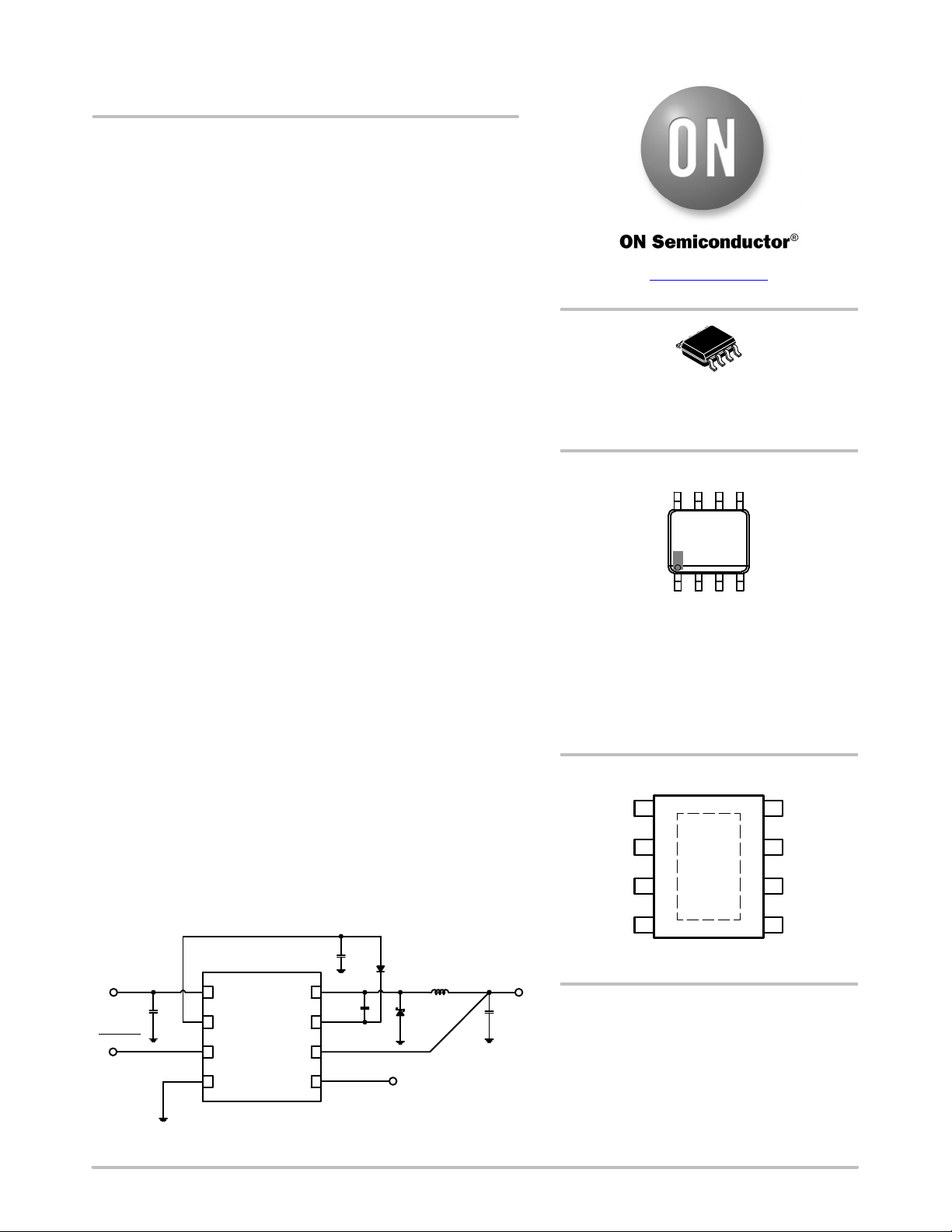
VIN
CIN
RESET
NCV891330
VIN
DRV
RSTB
GND EN
SW
BST
VOUT
CDRV
CBST
DBST
EN
DFW
L1
VOUT
COUT
www.onsemi.com
8
1
SOIC−8
EXPOSED PAD
CASE 751AC
MARKING DIAGRAM
8
891330XX
ALYW
G
1
With XX = 33 for 3.3 V Output
A = Assembly Location
L = Wafer Lot
Y = Year
W = Work Week
G = Pb−Free Device
VIN
DRV
RSTB
GND
ORDERING INFORMATION
See detailed ordering and shipping information on page 15 of
this data sheet.
= 38 for 3.8 V Output
= 40 for 4.0 V Output
= 50 for 5.0 V Output
PIN CONNECTIONS
1
2
3
4
(Top View)
8
7
6
5
SW
BST
VOUT
EN
Figure 1. Typical Application
© Semiconductor Components Industries, LLC, 2015
August, 2019 − Rev. 3
1 Publication Order Number:
NCV891330/D
Page 2
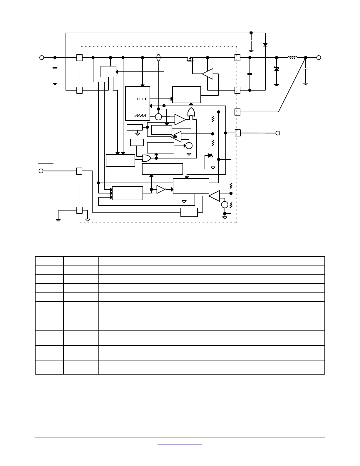
NCV891330
CDRV
DBST
VIN VOUT
VIN
SW
L1
CIN
RESET
DRV
RSTB
GND
3.3 V
Reg
VOLTAGES
MONITORS
SELECTION
Low
Oscillator
Enable
comp
TSD
MODE
NCV891330
+
+
S
3A
detector
Soft−Start
RESET
Switcher Supply
ON
PWM
LOGIC
ON
OFF
+
−
−
+
LINEAR
REGULATOR
ON
Logic
Figure 2. Simplified Block Diagram
+
OVLD
EN
DFW
COUT
CBST
BST
VOUT
EN
−
+
+
Table 1. PIN FUNCTION DESCRIPTION
Pin No. Pin Name Description
1 VIN Input voltage from battery. Place an input filter capacitor in close proximity to this pin.
2 DRV Output voltage to provide a regulated voltage to the Power Switch gate driver.
3 RSTB Reset function. Open drain output, pulling down to ground when the output voltage is out of regulation.
4 GND Battery return, and output voltage ground reference.
5 EN This TTL compatible Enable input allows the direct connection of Battery as the enable signal. Grounding
6 VOUT Output voltage feedback and LDO output. Feedback of output voltage used for regulation, as well as LDO
7 BST Bootstrap input provides drive voltage higher than VIN to the N−channel Power Switch for minimum
8 SW Switching node of the Regulator. Connect the output inductor and cathode of the freewheeling diode to
EPAD Connect to Pin 4 (electrical ground) and to a low thermal resistance path to the ambient temperature
this input stops switching and reduces quiescent current draw to a minimum.
output in LDO mode.
switch Rdson and highest efficiency.
this pin.
environment.
www.onsemi.com
2
Page 3
NCV891330
Table 2. ABSOLUTE MAXIMUM RATINGS
Rating Symbol Value Unit
Min/Max Voltage VIN −0.3 to 45 V
Max Voltage VIN to SW 45 V
Min/Max Voltage SW −0.7 to 40 V
Min Voltage SW − 20 ns −3.0 V
Min/Max Voltage EN −0.3 to 40 V
Min/Max Voltage BST −0.3 to 43 V
Min/Max Voltage BST to SW −0.3 to 3.6 V
Min/Max Voltage on RSTB −0.3 to 6 V
Min/Max Voltage VOUT −0.3 to 18 V
Min/Max Voltage DRV −0.3 to 3.6 V
Thermal Resistance, SOIC8−EP Junction–to–Ambient (Note 1) R
θ
JA
Storage Temperature range −55 to +150 °C
Operating Junction Temperature Range T
J
ESD withstand Voltage (Note 2) Human Body Model VESD 2.0 kV
Moisture Sensitivity MSL Level 2
Peak Reflow Soldering Temperature (Note 3) 260 °C
Stresses exceeding those listed in the Maximum Ratings table may damage the device. If any of these limits are exceeded, device functionality
should not be assumed, damage may occur and reliability may be affected.
1. Value based on 4 layers of 645 mm
2
(or 1 in2) of 1 oz copper thickness on FR4 PCB substrate.
2. This device series incorporates ESD protection and is tested by the following methods:
ESD Human Body Model tested per AEC−Q100−002 (EIA/JESD22−A114)
Latchup Current Maximum Rating: v150 mA per JEDEC standard: JESD78
3. For information, please refer to our Soldering and Mounting Techniques Reference Manual, SOLDERRM/D
30 °C/W
−40 to +150 °C
Table 3. ELECTRICAL CHARACTERISTICS
VIN = 4.5 to 28 V, VEN = 5 V, V
range −40°C v T
v 150°C unless noted otherwise, and are guaranteed by test, design or statistical correlation (Notes 4, 5)
J
Parameter
QUIESCENT CURRENT
Quiescent Current, enabled
Quiescent Current, shutdown VIN = 13.2 V, VEN = 0 V, 25°C I
UNDERVOLTAGE LOCKOUT – VIN (UVLO)
UVLO Start Threshold
UVLO Stop Threshold VIN falling V
UVLO Hysteresis V
SOFT−START (SS)
Soft−Start Completion Time
OUTPUT VOLTAGE
Output Voltage during regulation
OSCILLATOR
Frequency
4. Refer to ABSOLUTE MAXIMUM RATINGS and APPLICATION INFORMATION for Safe Operating Area.
5. Performance guaranteed over the indicated operating temperature range by design and/or characterization tested at T
duty cycle pulse techniques are used during testing to maintain the junction temperature as close to ambient as possible.
= VSW + 3 V, C
BST
= 0.1 mF, for typical values TJ = 25°C, Min/Max values are valid for the temperature
DRV
Test Conditions Symbol Min Typ Max Unit
VIN = 13.2 V, I
= 100 mA, 25°C
OUT
VIN rising V
100 mA < I
< 2.5 A
OUT
5.0 V option
4.0 V option
3.8 V option
3.3 V option
4.5 < VIN < 18 V
20 V <V
< 28V
IN
I
q
qSD
UVLSTT
UVLSTP
UVLOHY
t
SS
V
OUTreg
F
SW
F
SW(HV)
4.1 4.5 V
3.1 3.7 V
0.4 1.4 V
0.8 1.4 2.0 ms
4.9
3.92
3.724
3.234
1.8
0.9
30 39
9 12
5.0
4.0
3.8
3.3
2.0
1.0
mA
mA
V
5.1
4.08
3.876
3.366
2.2
MHz
1.1
= TA = 25°C. Low
J
www.onsemi.com
3
Page 4
NCV891330
Table 3. ELECTRICAL CHARACTERISTICS
VIN = 4.5 to 28 V, VEN = 5 V, V
range −40°C v T
v 150°C unless noted otherwise, and are guaranteed by test, design or statistical correlation (Notes 4, 5)
J
Parameter UnitMaxTypMinSymbolTest Conditions
VIN FREQUENCY FOLDBACK MONITOR
Frequency Foldback Threshold
rising
V
IN
VIN falling
Frequency Foldback Hysteresis V
MODE TRANSITION
Normal to Low−Iq mode Current Threshold
Mode Transition Duration
Switcher to Linear
Linear to Switcher
Minimum time in Normal Mode before
starting to monitor output current
Linear to switcher transition
at high Vin
at low Vin
PEAK CURRENT LIMIT
Current Limit Threshold
POWER SWITCH
ON Resistance
Leakage current VIN to SW VSW = 0, −40°C v TJ v 85°C I
Minimum ON Time Measured at SW pin t
Minimum OFF Time Measured at SW pin
SLOPE COMPENSATION
Ramp Slope
(With respect to switch current)
LOW POWER LINEAR REGULATOR
Line Regulation
Load Regulation VIN = 13.2 V, 0.1 mA < I
Power Supply Rejection V
Current Limit I
Output clamp current V
SHORT CIRCUIT DETECTOR
Switching frequency in short−circuit condition Analog Foldback
Analog foldback – high V
Hiccup Mode
RESET
Leakage current into RSTB pin
Output voltage threshold at which the RSTB
signal goes low
4. Refer to ABSOLUTE MAXIMUM RATINGS and APPLICATION INFORMATION for Safe Operating Area.
5. Performance guaranteed over the indicated operating temperature range by design and/or characterization tested at T
duty cycle pulse techniques are used during testing to maintain the junction temperature as close to ambient as possible.
= VSW + 3 V, C
BST
IN
= 0.1 mF, for typical values TJ = 25°C, Min/Max values are valid for the temperature
DRV
V
8 V < VIN < 28 V I
t
t
t
V
= 3.3 V
OUT
V
= VSW + 3.0 V R
BST
V
LINtoSW(HV)
V
LINtoSW(LV)
t
At F
= 2 MHz (normal)
SW
At FSW = 500 kHz (max duty cycle)
4.5 < VIN < 18 V
20 V <VIN < 28V
I
= 5 mA, 6 V < VIN < 18 V V
OUT
< 50 mA V
OUT
OUT(ripple)
OUT
V
OUT
V
OUT
V
OUT
= 0.5 Vp−p, F = 100 Hz PSRR 65 dB
= V
OUTreg(typ)
+ 10% I
= 0 V, 4.5 V < VIN < 18 V
= 0 V, 20 V <VIN < 28 V
decreasing
5.0 V option
S
F
V
4.0 V option
3.8 V option
3.3 V option
V
FLDUP
FLDDN
FLDHY
NtoL
SWtoLIN
LINtoSW
SWblank
I
LIM
DSON
LKSW
ONMIN
OFFMIN
S
ramp
ramp(HV)
REG(line)
REG(load)
LIN(lim)
CL(OUT)
F
SWAF
SWAFHV
F
SWHIC
I
RSTBlk
RESET
18.4
18
0.2 0.3 0.4 V
3 40 mA
300
1 2
500
19
3.6
3.9 4.4 4.9 A
180 360
45 70 ns
30
30
1.45
0.65
50 70
2.0
1.0
5 25 mV
5 35 mV
50 80 mA
0.5 1.0 1.5 mA
450
225
24
4.50
3.6
3.42
2.97
550
275
32
4.625
3.7
3.515
3.05
20
V
19.8
ms
ms
V
28
4.5
mW
10
mA
ns
2.8
A/ms
1.3
kHz
650
325
40
1 uA
V
4.75
3.8
3.61
3.14
= TA = 25°C. Low
J
www.onsemi.com
4
Page 5
NCV891330
Table 3. ELECTRICAL CHARACTERISTICS
VIN = 4.5 to 28 V, VEN = 5 V, V
range −40°C v T
v 150°C unless noted otherwise, and are guaranteed by test, design or statistical correlation (Notes 4, 5)
J
Parameter UnitMaxTypMinSymbolTest Conditions
RESET
Hysteresis on RSTB threshold
Noise−filtering delay From V
Restart Delay time From V
Low RSTB voltage R
GATE VOLTAGE SUPPLY (DRV pin)
Output Voltage
DRV UVLO START Threshold V
DRV UVLO STOP Threshold V
DRV UVLO Hysteresis V
DRV Current Limit V
VIN OVERVOLTAGE SHUTDOWN MONITOR
Overvoltage Stop Threshold
Overvoltage Start Threshold VIN decreasing V
Overvoltage Hysteresis V
ENABLE (EN)
Logic low threshold voltage
Logic high threshold voltage V
EN pin input current I
THERMAL SHUTDOWN
Activation Temperature
Reset temperature TSD
Hysteresis T
4. Refer to ABSOLUTE MAXIMUM RATINGS and APPLICATION INFORMATION for Safe Operating Area.
5. Performance guaranteed over the indicated operating temperature range by design and/or characterization tested at T
duty cycle pulse techniques are used during testing to maintain the junction temperature as close to ambient as possible.
Product parametric performance is indicated in the Electrical Characteristics for the listed test conditions, unless otherwise noted. Product
performance may not be indicated by the Electrical Characteristics if operated under different conditions.
= VSW + 3 V, C
BST
= 0.1 mF, for typical values TJ = 25°C, Min/Max values are valid for the temperature
DRV
V
increasing
OUT
5.0 V option
4.0 V option
3.8 V option
3.3 V option
OUT<VRESET
going low
OUT>VRESET+VREShys
high RSTB
RSTBpullup
DRV
= V
= 0 V I
to RSTB pin
/1 mA, V
OUTreg
to
OUT
> 1 V V
VIN increasing V
V
REShys
t
filter
t
delay
RSTBlow
V
DRV
DRVSTT
DRVSTP
DRVHYS
DRVLIM
OVSTP
OVSTT
OVHY
V
ENlow
ENhigh
ENbias
25
20
19
17
60
50
45
40
10 25
14 16 18 ms
3.1 3.3 3.5 V
2.7 2.9 3.05 V
2.5 2.8 3.0 V
50 200 mV
21 50 mA
36.5 37.7 39.0 V
36.0 37.3 38.8 V
0.25 0.40 0.50 V
0.8 V
0.2 1
TSD 155 190 °C
restart
HYS
135 185 °C
5 20 °C
J
100
mV
80
76
66
ms
0.4 V
2 V
mA
= TA = 25°C. Low
www.onsemi.com
5
Page 6
NCV891330
TYPICAL CHARACTERISTICS
80
70
60
50
40
30
20
10
NO LOAD INPUT CURRENT (mA)
0
INPUT VOLTAGE (V)
Figure 3. No−load Input Current at TJ = 255C
vs. Input Voltage
100
80
60
40
1000
800
600
400
INPUT CURRENT (mA)
200
20151050
0
OUTPUT CURRENT (mA)
10008006004002000
Figure 4. Input Current at TJ = 255C vs. Output
Current
13
12
11
10
9
20
Iq IN LOW−Iq LINEAR MODE (mA)
0
TEMPERATURE (°C) TEMPERATURE (°C)
Figure 5. Low−Iq Mode Quiescent Current vs.
Junction Temperature
1.6
1.5
1.4
1.3
Iq IN SWITCHER MODE (mA)
1.2
TEMPERATURE (°C) TEMPERATURE (°C)
Figure 7. Switching Mode Quiescent Current
vs. Junction Temperature
8
Iq IN SHUTDOWN MODE (mA)
150100500−50
7
150100500−50
Figure 6. Shutdown Mode Quiescent Current
vs. Junction Temperature
3.36
3.34
3.32
Switcher Mode
3.30
3.28
3.26
3.3 V OUTPUT VOLTAGE (V)
150100500−50
3.24
Low−Iq Mode
150100500−50
Figure 8. 3.3 V Output Voltage vs. Junction
Temperature
www.onsemi.com
6
Page 7

NCV891330
TYPICAL CHARACTERISTICS
4.05
4.04
4.03
4.02
4.01
4.00
3.99
3.98
3.97
3.96
4 V OUTPUT VOLTAGE (V)
3.95
3.94
2.2
2.1
2.0
Switcher Mode
Low−Iq Mode
TEMPERATURE (°C)
Figure 9. 4.0 V Output Voltage vs. Junction
Temperature
5.05
5.04
5.03
5.02
5.01
Switcher Mode
5.00
4.99
4.98
Low−Iq Mode
4.97
4.96
5 V OUTPUT VOLTAGE (V)
4.95
150100500−50
4.94
TEMPERATURE (°C)
150100500−50
Figure 10. 5.0 V Output Voltage vs. Junction
Temperature
57
56
55
54
1.9
SWITCHING FREQUENCY (MHz)
1.8
TEMPERATURE (°C) TEMPERATURE (°C)
Figure 11. Switching Frequency vs. Junction
Temperature
56
54
52
50
MINIMUM OFF TIME (ns)
48
TEMPERATURE (°C) TEMPERATURE (°C)
Figure 13. Minimum Off Time vs. Junction
Temperature
MINIMUM ON TIME (ns)
53
150100500−50
150100500−50
52
4.7
4.6
4.5
4.4
4.3
PEAK CURRENT LIMIT (A)
4.2
150100500−50
Figure 12. Minimum On Time vs. Junction
Temperature
150100500−50
Figure 14. Peak Current Limit vs. Junction
Temperature
www.onsemi.com
7
Page 8

NCV891330
TYPICAL CHARACTERISTICS
4.6
4.4
4.2
4.0
3.8
3.6
3.4
UVLO THRESHOLDS (V)
3.2
3.0
Figure 15. UVLO Thresholds vs. Junction
1.60
1.55
1.50
1.45
SOFT−START TIME (ms)
40
Start−up Threshold
UVLO Threshold
150100500−50
TEMPERATURE (°C) TEMPERATURE (°C)
39
38
37
36
35
OVERVOLTAGE THRESHOLDS (V)
34
Overvoltage Threshold
Restart Threshold
Figure 16. Input Overvoltage Thresholds vs.
Temperature
3.5
3.4
3.3
3.2
DRV VOLTAGE (V)
3.1
Junction Temperature
I
= 0 mA
DRV
I
= 21 mA
DRV
150100500−50
1.40
TEMPERATURE (°C) TEMPERATURE (°C)
Figure 17. Soft−start Duration vs. Junction
3.0
2.9
2.8
2.7
DRV UVLO THRESHOLDS (V)
2.6
TEMPERATURE (°C) TEMPERATURE (°C)
Figure 19. DRV Voltage UVLO Tresholds vs.
Junction Temperature
Temperature
DRV Start−up Threshold
DRV UVLO Threshold
150100500−50
150100500−50
3.0
19.8
19.6
19.4
19.2
THRESHOLDS (V)
IN
19.0
18.8
18.6
18.4
18.2
18.0
FREQUENCY FOLDBACK V
150100500−50
Figure 18. DRV Voltage vs. Junction
Temperature
VIN Rising
VIN Falling
150100500−50
Figure 20. Frequency Foldback Voltage
Tresholds vs. Junction Temperature
www.onsemi.com
8
Page 9

NCV891330
TYPICAL CHARACTERISTICS
1.10
(MHz)
IN
1.05
1.00
0.95
0.90
SWITCHING FREQUENCY AT HIGH V
TEMPERATURE (°C) TEMPERATURE (°C)
Figure 21. Foldback Frequency vs. Junction
Temperature
4.0
3.9
3.8
3.7
THRESHOLDS (V)
OUT
3.6
3.5
4 V RESET V
3.4
RSTB Toggles High (V
RSTB Toggles Low (V
TEMPERATURE (°C)
OUT
OUT
Rising)
Falling)
Figure 23. 4.0 V Version RESET Thresholds vs.
Junction Temperature
THRESHOLDS (V)5 V RESET V
OUT
3.3 V RESET V
150100500−50
THRESHOLDS (V)
OUT
150100500−50
3.3
3.2
RSTB Toggles High (V
3.1
RSTB Toggles Low (V
3.0
2.9
2.8
OUT
OUT
Rising)
Falling)
Figure 22. 3.3 V Version RESET Thresholds vs.
Junction Temperature
5.0
4.9
4.8
4.7
4.6
4.5
4.4
4.3
RSTB Toggles High (V
RSTB Toggles Low (V
TEMPERATURE (°C)
OUT
OUT
Rising)
Falling)
Figure 24. 5.0 V Version RESET Thresholds vs.
Junction Temperature
150100500−50
150100500−50
17.0
16.8
16.6
16.4
16.2
16.0
RESET DELAY (ms)
15.8
15.6
15.4
TEMPERATURE (°C) TEMPERATURE (°C)
Figure 25. RESET Delay vs. Junction
Temperature
71
69
67
65
63
61
59
CURRENT THRESHOLD (mA)
LINEAR TO SWITCHER MODE
57
150100500−50
55
www.onsemi.com
9
150100500−50
Figure 26. Low−Iq to Switcher Mode Transition
vs. Junction Temperature
Page 10

NCV891330
TYPICAL CHARACTERISTICS
30
20
10
CURRENT RANGE FOR LOW−Iq
TRANSITION − 3.3 V VERSION (mA)
0
510 18
INPUT VOLTAGE (V) INPUT VOLTAGE (V)
15
Figure 27. Switcher to Low−Iq Mode Transition
(3.3 V Version, 2.2 mH) vs. Input Voltage
30
20
10
CURRENT RANGE FOR LOW−Iq
TRANSITION − 5 V VERSION (mA)
0
510 18
15
Figure 28. Switcher to Low−Iq Mode Transition
(5.0 V Version, 2.2 mH) vs. Input Voltage
www.onsemi.com
10
Page 11

NCV891330
APPLICATION INFORMATION
Hybrid Low−Power Mode
A high−frequency switch−mode regulator is not very
efficient in light load conditions, making it difficult to
achieve low−Iq requirements for sleep−mode operation. To
remedy this, the NCV891330 includes a low−Iq linear
regulator that turns on at light load, while the PWM
regulator turns off, ensuring a high−efficiency low−power
operation. Another advantage of linear mode is the tight
regulation free of voltage ripple usually associated with
low−Iq switchers in light load conditions.
At initial start−up the NCV891330 always runs in PWM
converter mode, regardless of the output current, and goes
through a soft start. It then stays in PWM mode if the output
current is high enough. If the output current is low, the
NCV891330 transitions to Linear Regulator mode, after a
300 ms period during which it assesses the level of ouput
current. Note that the Reset signal needs to be high before the
IC starts to look at the output current level.
It stays in this low−power mode until the output current
exceeds the I
limit: it then transitions to PWM
LIN(lim)
SWITCH
converter mode. This transition happens in less than 2 ms, so
that the transient response is not affected by the mode change
Once the NCV891330 has transitioned to switcher mode,
it cannot go back to low−Iq mode before a 500 ms blanking
period has elapsed, after which it starts looking at the output
current level.
If the NCV891330 is in low−Iq Linear Regulator mode in
normal battery range, it will transition to switcher mode
when VIN increases above V
LINtoSW(HV)
, regardless of the
output current. Similarly, if the NCV891330 is in PWM
mode and V
is higher than V
IN
, it will not transition
FLDUP
to low−Iq Linear mode even if the output current becomes
lower than I
NtoL
.
At low input voltage, the NCV891330 stays in low−Iq
mode down to V
LINtoSW(LV)
if it entered this mode while in
normal battery range. However it may not enter low−Iq
mode below 8 V depending on the charge of the bootstrap
capacitor (see Bootstrap section and typical characteristics
curves for details).
.
50 mA
I
LIN(lim)
80 mA
I
I
NtoL
MODE
LOW−IQ
Figure 29. Mode Transition Diagram for Input Voltages between 8.0 V and V
3 mA
NO MODE TRANSITION
40 mA
Output Current
OUT
LINtoSW(HV)
www.onsemi.com
11
Page 12

NCV891330
Input Voltage
An Undervoltage Lockout (UVLO) circuit monitors the
input. The circuit can inhibit switching and reset the
Soft−start circuit if there is insufficient voltage for proper
regulation. Depending on the output conditions (voltage
option and loading), the NCV891330 may lose regulation
and run in drop−out mode before reaching the UVLO
threshold: refer to the Minimum Vin calculation tool for
details. When the input voltage drops low enough that the
part cannot regulate because it reaches its maximum duty
cycle, the switching frequency is divided down by up to 4
(down to 500 kHz). This helps lowering the minimum
voltage at which the regulator loses regulation.
F
SW
(MHz)
2
Frequency
folds back
if drop−out
mode
1
An overvoltage monitoring circuit automatically
terminates switching if the input voltage exceeds V
OVSTP
(see Figure 30), but the NCV891330 can withstand input
voltages up to 45 V.
To avoid skipping switching pulses and entering an
uncontrolled mode of operation, the switching frequency is
reduced by a factor of 2 when the input voltage exceeds the
V
Frequency Foldback threshold (see Figure 30).
IN
Frequency reduction is automatically terminated when the
input voltage drops back below the V
Frequency Foldback
IN
threshold. This also helps to limit the power lost in switching
and generating the drive voltage for the Power Switch.
3.5 18 20 36
Figure 30. NCV891330 Switching Frequency Profile vs. Input Voltage
Soft−Start
Upon being enabled or released from a fault condition,
and after the DRV voltage is established, a soft−start circuit
ramps the switching regulator error amplifier reference
voltage to the final value. During soft−start, the average
switching frequency is lower until the output voltage
approaches regulation.
Slope Compensation
A fixed slope compensation signal is generated internally
and added to the sensed current to avoid increased output
voltage ripple due to bifurcation of inductor ripple current
at duty cycles above 50%. The fixed amplitude of the slope
4539
(V)
V
IN
compensation signal requires the inductor to be greater than
a minimum value, depending on output voltage, in order to
avoid sub−harmonic oscillations. The recommended inductor
values are 2.2 or 3.3 mH, although higher values are possible.
Current Limiting
Due to the ripple on the inductor current, the average
output current of a buck converter is lower than the peak
current setpoint of the regulator. Figure 31 shows – for a
2.2 mH inductor – how the variation of inductor peak current
with input voltage affects the maximum DC current the
NCV891330 can deliver to a load.
www.onsemi.com
12
Page 13

NCV891330
Figure 31. NCV891330 Load Current Capability with a 2.2 mH Inductor
Short Circuit Protection
During severe output overloads or short circuits, the
NCV891330 automatically reduces its switching frequency.
This creates duty cycles small enough to limit the peak
current in the power components, while maintaining the
ability to automatically reestablish the output voltage if the
overload is removed.
In more severe short−circuit conditions where the inductor
current is still too high after the switching frequency has fully
folded back, the regulator enters a hiccup mode that further
reduces the power dissipation and protects the system.
RESET Function
The RSTB pin is pulled low when the output voltage falls
below 7.5% of the nominal regulation level, and floats when
the output is properly regulated. A pull−up resistor tied to the
output is needed to generate a logic high signal on this open
drain pin. The pin can be left unconnected when not used.
When the output voltage drops out of regulation, the pin
goes low after a short noise−filtering delay (t
for a 16 ms delay time after the output goes back to regulation,
simplifying the connection to a micro−controller.
). It stays low
filter
The RSTB pin is also pulled low immediately in case of VIN
overvoltage, Thermal shutdown, VIN UVLO or DRV UVLO.
Feedback Loop
All components of the feedback loop (output voltage
sensing, error amplifier and compensation) are integrated
inside the NCV891330, and are optimized to ensure
regulation and sufficient phase and gain margin for the
recommended conditions of operation.
Recommended conditions and components:
• Input: car battery
• Output: 3.3 V, 3.8 V, 4 V or 5 V, with output current up
to 3 A
• Output capacitor: 30 mF capacitance
• Inductor: 2.2 mH to 3.3 mH
With these operating conditions and components, the
open loop transfer function has a phase margin greater than
50°, as can be seen in Figure 32.
www.onsemi.com
13
Page 14

NCV891330
Figure 32. Bode Plot of the Open Loop Transfer Function of a Buck Converter using the
NCV891330 for Vin = 13 V, Vout = 3.3 V, Iout = 2 A, Cout=3x10 mF and L=2.2 mH
For more details and for effect of component values other
than the recommended ones, please refer to the design
spreadsheet provided on the www.onsemi.com
NCV891330
page.
The design spreadsheet also includes the total open loop
transfer function for the output voltage sensing at the
NCV891330 VOUT pin to the output voltage.
www.onsemi.com
14
Page 15

NCV891330
Bootstrap
At the DRV pin an internal regulator provides a ground−
referenced voltage to an external capacitor (C
fast recharge of the external bootstrap capacitor (C
DRV
), to allow
) used
BST
to supply power to the power switch gate driver. If the
voltage at the DRV pin goes below the DRV UVLO
Threshold V
, switching is inhibited and the
DRVSTP
Soft−start circuit is reset, until the DRV pin voltage goes
back up above V
DRVSTT
.
The NCV891330 permanently monitors the bootstrap
capacitor, and always ensures it stays charged no matter
what the operating conditions are. As a result, the additional
charging current for the bootstrap capacitor may prevent the
regulator from entering Low−Iq mode at low input voltage.
Practically, the 5 V output version does not enter Low−Iq
mode for input voltages below 8 V, and the 3.8 V and 4 V
versions for input voltages below 6.5 V (see typical
characteristics curves for details).
Enable
voltages above 40 V are expected, EN should be tied to VIN
through a 10 kW resistor in order to limit the current flowing
into the overvoltage protection of the pin.
EN low induces a shutdown mode which shuts off the
regulator and minimizes its supply current to 9 mA typical by
disabling all functions.
Upon enabling, voltage is established at the DRV pin,
followed by a soft−start of the switching regulator output.
Thermal Shutdown
A thermal shutdown circuit inhibits switching, resets the
Soft−start circuit, and removes DRV voltage if internal
temperature exceeds a safe level. Switching is automatically
restored when temperature returns to a safe level.
Exposed Pad
The exposed pad (EPAD) on the back of the package must
be electrically connected to the electrical ground (GND pin)
for proper, noise−free operation.
The NCV891330 is designed to accept either a logic level
signal or battery voltage as an Enable signal. However if
ORDERING INFORMATION
Device Output Package Shipping
NCV891330PD50R2G 5.0 V
NCV891330PD40R2G 4.0 V
NCV891330PD38R2G 3.8 V
NCV891330PD33R2G 3.3 V
†For information on tape and reel specifications, including part orientation and tape sizes, please refer to our Tape and Reel Packaging
Specifications Brochure, BRD8011/D.
SOIC−8 EP
(Pb−Free)
2500 / Tape & Reel
www.onsemi.com
15
Page 16

MECHANICAL CASE OUTLINE
PACKAGE DIMENSIONS
8
1
SCALE 1:1
SOIC−8 EP
CASE 751AC
ISSUE D
DATE 02 APR 2019
GENERIC
MARKING DIAGRAM*
8
XXXXX
AYWWG
G
1
DOCUMENT NUMBER:
DESCRIPTION:
ON Semiconductor and are trademarks of Semiconductor Components Industries, LLC dba ON Semiconductor or its subsidiaries in the United States and/or other countries.
ON Semiconductor reserves the right to make changes without further notice to any products herein. ON Semiconductor makes no warranty, representation or guarantee regarding
the suitability of its products for any particular purpose, nor does ON Semiconductor assume any liability arising out of the application or use of any product or circuit, and specifically
disclaims any and all liability, including without limitation special, consequential or incidental damages. ON Semiconductor does not convey any license under its patent rights nor the
rights of others.
© Semiconductor Components Industries, LLC, 2018
XXXXXX = Specific Device Code
A = Assembly Location
Y = Year
WW = Work Week
G = Pb−Free Package
98AON14029D
SOIC−8 EP
Electronic versions are uncontrolled except when accessed directly from the Document Repository.
Printed versions are uncontrolled except when stamped “CONTROLLED COPY” in red.
*This information is generic. Please refer to
device data sheet for actual part marking.
Pb−Free indicator, “G” or microdot “ G”, may
or may not be present and may be in either
location. Some products may not follow the
Generic Marking.
PAGE 1 OF 1
www.onsemi.com
Page 17

ON Semiconductor and are trademarks of Semiconductor Components Industries, LLC dba ON Semiconductor or its subsidiaries in the United States and/or other countries.
ON Semiconductor owns the rights to a number of patents, trademarks, copyrights, trade secrets, and other intellectual property. A listing of ON Semiconductor’s product/patent
coverage may be accessed at www.onsemi.com/site/pdf/Patent−Marking.pdf
ON Semiconductor makes no warranty, representation or guarantee regarding the suitability of its products for any particular purpose, nor does ON Semiconductor assume any liability
arising out of the application or use of any product or circuit, and specifically disclaims any and all liability, including without limitation special, consequential or incidental damages.
Buyer is responsible for its products and applications using ON Semiconductor products, including compliance with all laws, regulations and safety requirements or standards,
regardless of any support or applications information provided by ON Semiconductor. “Typical” parameters which may be provided in ON Semiconductor data sheets and/or
specifications can and do vary in different applications and actual performance may vary over time. All operating parameters, including “Typicals” must be validated for each customer
application by customer’s technical experts. ON Semiconductor does not convey any license under its patent rights nor the rights of others. ON Semiconductor products are not
designed, intended, or authorized for use as a critical component in life support systems or any FDA Class 3 medical devices or medical devices with a same or similar classification
in a foreign jurisdiction or any devices intended for implantation in the human body. Should Buyer purchase or use ON Semiconductor products for any such unintended or unauthorized
application, Buyer shall indemnify and hold ON Semiconductor and its officers, employees, subsidiaries, affiliates, and distributors harmless against all claims, costs, damages, and
expenses, and reasonable attorney fees arising out of, directly or indirectly, any claim of personal injury or death associated with such unintended or unauthorized use, even if such
claim alleges that ON Semiconductor was negligent regarding the design or manufacture of the part. ON Semiconductor is an Equal Opportunity/Affirmative Action Employer. This
literature is subject to all applicable copyright laws and is not for resale in any manner.
. ON Semiconductor reserves the right to make changes without further notice to any products herein.
PUBLICATION ORDERING INFORMATION
LITERATURE FULFILLMENT:
Email Requests to: orderlit@onsemi.com
ON Semiconductor Website: www.onsemi.com
TECHNICAL SUPPORT
North American Technical Support:
Voice Mail: 1 800−282−9855 Toll Free USA/Canada
Phone: 011 421 33 790 2910
Europe, Middle East and Africa Technical Support:
Phone: 00421 33 790 2910
For additional information, please contact your local Sales Representative
◊
www.onsemi.com
1
 Loading...