

Page 1
NCV891234, NCV891334
NCV891234, NCV891334
Evaluation Board
User'sManual
Description
The NCV891x34 is a Dual Mode regulator intended for
Automotive, battery−connected applications. The output is
fixed to either 3.3 V or 5.0 V, capable of delivering 2.0 A
(NCV891234) or 3.0 A (NCV891334). At low output
currents (≤ 50 mA), the device will operate in LDO mode,
switching to PWM mode as current increases beyond
50 mA. The device is equipped with SYNCI and SYNCO
pins to synchronize to an external clock and/or another
NCV891x34. A reset (with fixed delay) and a fault pin
(flagging low input voltage and high temperature warnings)
simplify interfacing with a microcontroller.
www.onsemi.com
EVAL BOARD USER’S MANUAL
This document will help the user to set up the hardware
and to make demonstration kit running. All evaluation kit
components will be described (evaluation board,
connections, jumper’s configuration). A quick test
procedure will be also described to guide the user.
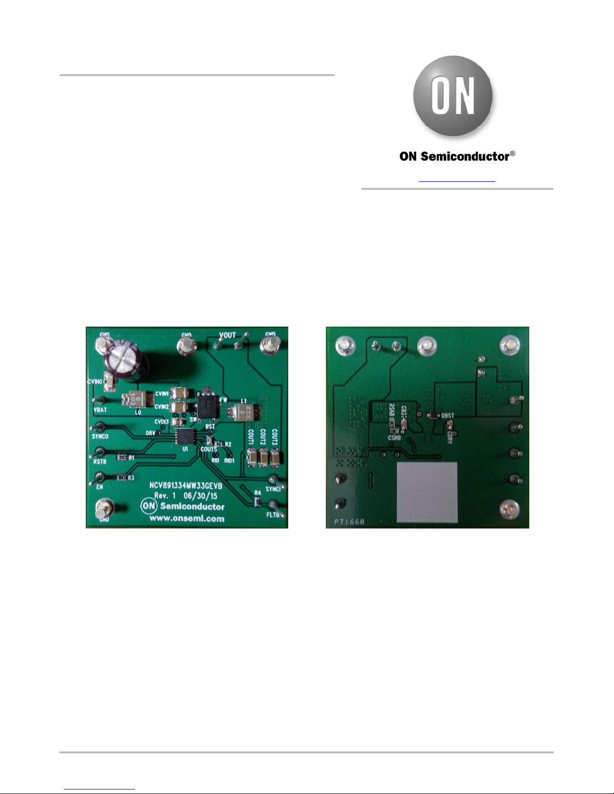
Top Side Bottom Side
Features and Benefits
• 40 mA Iq in Light Load Condition
• 2.0 A Maximum Output Current in PWM Mode in
NCV891234
• 3.0 A Maximum Output Current in PWM Mode in
NCV891334
• Internal N−channel Power Switch
• V
Operating Range 3.7 V to 36 V, Withstands Load
IN
Dump to 45 V
• Logic Level Enable Pin can be Tied to Battery
© Semiconductor Components Industries, LLC, 2016
November, 2016 − Rev. 0
Figure 1. Evaluation Board Photo
• Fixed Output Voltage of 5.0 V or 3.3 V with ±2%
Accuracy
• 2 MHz Free−running Switching Frequency
• Input and Output Synchronization Pins
Typical Applications
• Safety – Vision Systems
• Audio, Infotainment
• Instrumentation
• Telematics
1 Publication Order Number:
EVBUM2492/D
Page 2
NCV891234, NCV891334
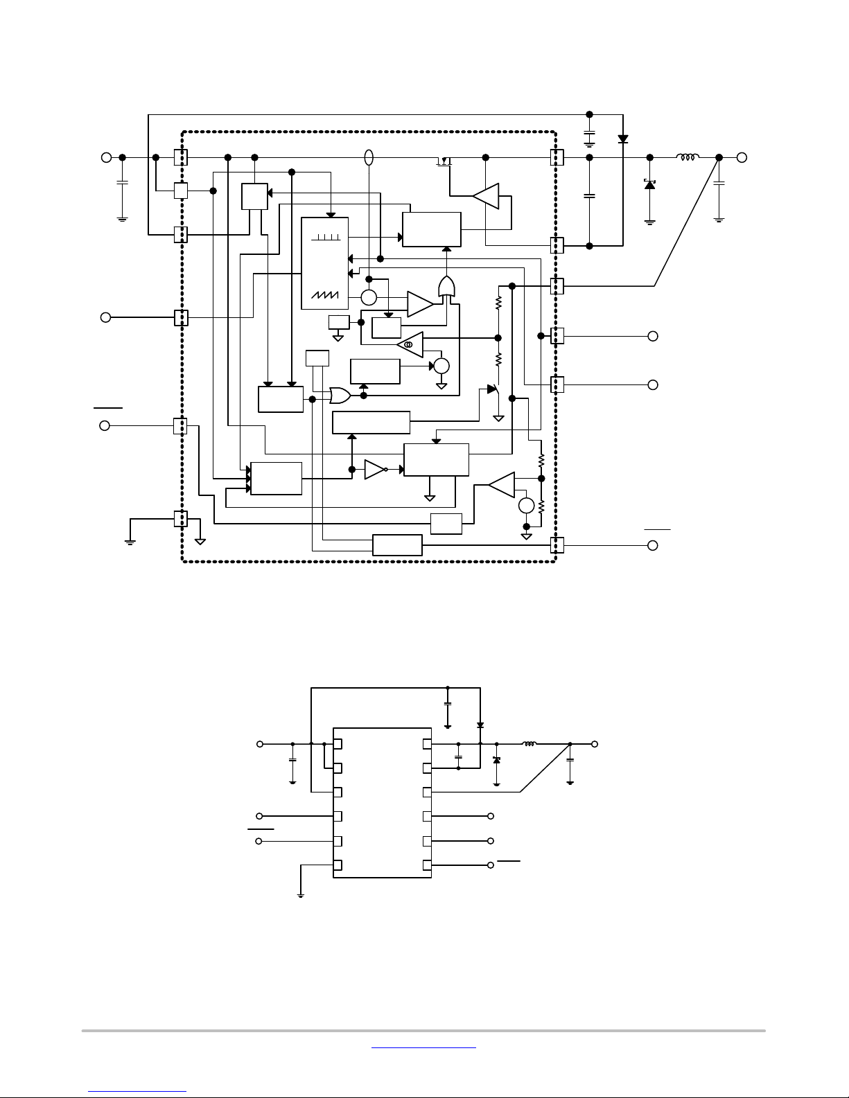
BLOCK DIAGRAM
CDRV
VIN VOUT
CIN
SYNCO
RESET
VIN
VIN2
DRV
SYNCO
RSTB
3.3 V
Reg
VOLTAGES
MONITORS
MODE
SELECTION
Oscillator
Enable
Sync
Sync
Out
comp
TSD
In
+
+
S
2A, 3A
detector
Soft−Start
RESET
Switcher Supply
ON
Low
PWM
LOGIC
ON
+
−
−
+
LINEAR
REGULATOR
ON
OFF
+
OVLD
−
+
GND
Logic
Fault
NCV891234, NCV891334
Detection
SW
BST
VOUT
EN
SYNCI
+
FLTB
CBST
DBST
DFW
EN
SYNCI
FAULT
L1
COUT
Figure 2. NCV891x34 Simplified Block Diagram
TYPICAL APPLICATION
CDRV
DBST
VIN VOUT
CIN
SYNCO
RESET
Figure 3. NCV891x34 Typical Application Diagram
VIN
VIN 2
DRV
SYNCO
GND
NCV891x34
VOUT
SYNCIRSTB
FLTB
SW
BST
L1
CBST
EN
DFW
ENABLE
SYNCI
FAULT
COUT
www.onsemi.com
2
Page 3
NCV891234, NCV891334
Table 1. EVALUATION BOARD TERMINALS
Pin Number Pin Name Function
1 VBAT Input voltage from battery. Place an input filter capacitor in close proximity to this pin.
4 SYNCO Out−of−phase synchronization output. Turn−on of the Power Switch causes the SYNCO signal to
5 RSTB Reset function. Open drain output, pulling down to ground when output voltage is out of regulation.
6 GND Battery return and output voltage ground reference.
7 FLTB Fault flag indicating various fault conditions for the part.
8 SYNCI Synchronization input. Connecting an external clock to this pin synchronizes switching to the rising
9 EN This TTL compatible Enable input allows the direct connection of Battery as the enable signal.
10 VOUT Output voltage feedback and LDO output. Feedback of output voltage used for regulation, as well
Table 2. ABSOLUTE MAXIMUM RATINGS
(Voltages are with respect to GND)
DC supply voltage (VBAT) −0.3 to 45 V
DC supply voltage (EN) −0.3 to 40 V
DC supply voltage (VOUT) −0.3 to 18 V
DC supply voltage (SYNCI, RSTB, and FLTB) −0.3 to 6 V
DC supply voltage (SYNCO) −0.3 to 3.6 V
Storage Temperature Range −55 to +150 °C
Stresses exceeding those listed in the Maximum Ratings table may damage the device. If any of these limits are exceeded, device functionality
should not be assumed, damage may occur and reliability may be affected.
fall (and rise half a switching period later).
edge of the SYNCI signal.
Grounding this signal stops switching and reduces quiescent current draw to a minimum.
as LDO output in LDO mode.
Rating
Value Units
Table 3. ELECTRICAL CHARACTERISTICS
Characteristics Conditions Typical Value Units
Regulation
Output Voltage (NCV891x34MW33GEVB)
Output Voltage (NCV891x34MW50GEVB) 5.0 V
Switching
Switching Frequency
Soft−start Time 1.4 ms
Synchronization Frequency Range 1.8 to 2.5 MHz
Current Limit
Peak Current Limit (NCV891234MWxxGEVB)
Peak Current Limit (NCV891334MWxxGEVB) 4.4 A
Protections
V
Input Undervoltage Lockout (UVLO)
Input Overvoltage Protection V
Thermal Shutdown TJ rising 170 °C
Product parametric performance is indicated in the Electrical Characteristics for the listed test conditions, unless otherwise noted. Product
performance may not be indicated by the Electrical Characteristics if operated under different conditions.
decreasing 3.1 V
BAT
increasing 37.7 V
BAT
3.3 V
2.0 MHz
3.25 A
www.onsemi.com
3
Page 4

NCV891234, NCV891334
Quick−Start Guide
The following steps will get you familiar with the setup of
inputs and outputs of the NCV891x34.
Required Equipment
1 DC Source – ≥ 40 V, ≥ 2 A capable VBAT
1 Oscilloscope – 2 Channel minimum VOUT and SW
1 Multi−meter VOUT
1 DC Electronic Load – 4 A capable ILOAD
1 Clip to Clip Lead or equivalent
1. Connect DC source set to 13.2 V DC between the
VBAT and GND terminals in the upper left of the
evaluation board.
2. Connect a multi−meter or oscilloscope probe
between the VOUT and GND terminals located in
the upper right of the evaluation board.
3. Connect an oscilloscope probe between the SW
and GND terminals located in the center of the
evaluation board.
4. Connect a jumper wire between VBAT to the EN
input.
Verify that VOUT is:
a.) 3.3 V for NCV891x34MW33GEVB
b.) 5.0 V for NCV891x34MW50GEVB
5. Apply a 40 mA load to VOUT.
Verify that VOUT is at the necessary regulated
voltage and the SW signal shows that DC level
(LDO mode).
6. Increase the load on VOUT to 1.5 A.
Verify that VOUT is at the necessary regulated
voltage and the SW signal shows a stable 2 MHz
pulsed waveform with amplitude approximately
between VBAT and GND (PWM mode).
7. While at load, increase VBAT to 21 V.
Verify that the SW signal now shows a stable
1 MHz pulsed waveform with amplitude
approximately between VBAT and GND.
8. Increase VBAT to 39.5 V.
Verify the switching regulator turns off and there is
0 V at VOUT.
9. Reduce VBAT to 13.2 V.
Verify that VOUT is restored to its previous value
and that the SW signal returns to a 2 MHz pulsed
waveform with amplitude approximately between
VBAT and GND.
10. Remove the load on VOUT.
Verify that VOUT is at the necessary regulated
voltage and the SW signal shows that DC level
(LDO mode).
11. Remove the jumper between VBAT the EN input.
Verify the switching regulator turns off and there is
0 V at VOUT.
12. Disconnect VBAT from the board.
Soft Start
The NCV891x34 contains a battery−connectable EN pin
for the primary buck regulator. A common setup includes the
following connections:
EN → VIN
When the EN connection on the board are as shown above,
the following startup profile can be seen on an oscilloscope:
Figure 4. Typical NCV891x34 Startup Profile
www.onsemi.com
4
Page 5

NCV891234, NCV891334
EMI Filter
In a typical application, an LC filter is used on the input
line of a buck regulator to filter EMI from the device. On this
evaluation board, an LC filter is pre−populated to allow you
to perform EMI testing directly with this evaluation board.
Figure 5. LC Filter on VIN Line
L0: 1.0 mH
CVIN0: 4.7 mF
CB1: 100 mF
An input filter can drastically reduce the emissions from
a switching regulator.
Efficiency
Figure 6. NCV891x34 Efficiency Curves
www.onsemi.com
5
Page 6

NCV891234, NCV891334
SCHEMATIC
Figure 7. NCV891x34MWxxGEVB Evaluation Board Schematic − Rev.1
www.onsemi.com
6
Page 7

NCV891234, NCV891334
PCB LAYOUT
Figure 8. NCV891334MW50GEVB PCB Layout − Top
Figure 9. NCV891334MW50GEVB PCB Layout − Bottom
All evaluation board PCB layouts are identical with the
exception of TOP Silkscreen and device mounted upon
them.
www.onsemi.com
7
Page 8

NCV891234, NCV891334
BILL OF MATERIALS
Table 4. BILL OF MATERIALS
Reference
Designator(s)
CVIN0 1 CAP CER 0.1UF 250V
CVIN1, CVIN2 2 CAP CER 4.7UF 50V 10%
CVIN3 1 CAP CER 1.0UF 50V X7R
CB1 1 CAP ALUM 100UF 63V
CBST, CDRV,
COUTS
COUT1,
COUT2, COUT3
CSNB 1 CAP CER 100pF 50V 5%
R1, R3, R4 3 RES 10.0K OHM 1/10W
R2 1 RES 0.0 OHM 1/10W
RSNB 1 RES 10.0 OHM 1/10W
DFW 1 DIODE SCHOTTKY 4.0A
DBST 1 DIODE SWITCH 200MA
L0 1 High Current Shielded
L1 1 High Current Shielded
GND1, GND2,
GND3, GND4
EN, FAULTB,
RSTB, SYNCI,
SYNCO, VBAT,
VOUT1, VOUT2
BST, DRV,
RID1, RID2, SW
U1 * 1 Automotive Buck
Qty Description Value
10% X7R 1210
X7R 1210
0805
20% RADIAL
3 CAP .10UF 16V
3 CAP CER 10UF 10V X7R
CERAMIC X7R 0603
1206
NP0 603
1% 0603 SMD
0603 SMD
0603 SMD
40V SMB
100V SOD323
Inductor 1.0uH, 8.7A SAT
Inductor 2.2uH, 5.6A SAT
4 TERM SOLDER TURRET
8 PIN INBOARD .042”
5 CIRCUIT PIN PRNTD
.219”, .109”L
HOLE 1000/PKG
.020”D .425”L
Switching Regulator
0.1 mF
4.7 mF
1.0 mF
100 mF
0.1 mF
10 mF
Do Not
Populate
10.0 K 1% 603 Vishay/Dale CRCW060310K0FKEA
0.0 N/A 603 Vishay/Dale CRCW06030000Z0EA
Do Not
Populate
40 V /
4.0 A
100 V /
0.2 A
1.0 mH
2.2 mH
N/A N/A TURRET Mill−Max
N/A N/A TP Vector Electronics K24C/M
Do Not
Populate
*The Bills of Materials for all four evaluation boards covered in this user’s manual are identical with the exception of the mounted device.
This can be either NCV891234MW33R2G, NCV891234MW50R2G, NCV891334MW33R2G, or NCV891334MW50R2G.
Toler-
ance
Foot-
print
10% 1210 TDK Corporation CGA6M3X7R2E104K200AA
10% 1210 Murata Electronics
10% 805 Murata Electronics
20% CAP_RAD
_8X11P5
10% 603 Murata Electronics
10% 1206 Murata Electronics
5% 603 Murata Electronics
1% 603 Vishay/Dale CRCW060310R0FKEA
N/A MBR340MFSON Semiconductor NRVB440MFST1G
N/A SOD_323 ON Semiconductor BAS16HT1G
20% XAL4020−
20% XAL4020−
102ME
222ME
N/A SMALLTP Mill−Max
* N/A 12PINDF
N4X4P65
Manufacturer’s Part
Manufacturer
North America
North America
Chemi−Con ELXZ630ELL101MH15D
North America
North America
North America
Coilcraft XAL4020−102ME
Coilcraft XAL4020−222ME
Manufacturing Corp.
Manufacturing Corp.
ON Semiconductor NCV891x34MWxxR2G
Number
GCM32ER71H475KA55L
GCM21BR71H105KA03L
GCM188R71C104KA37D
GCM31CR71A106KA64L
GCM1885C1H101JA16D
2501−2−00−44−00−00−07−0
3128−2−00−15−00−00−08−0
ON Semiconductor and are trademarks of Semiconductor Components Industries, LLC dba ON Semiconductor or its subsidiaries in the United States and/or other countries.
ON Semiconductor owns the rights to a number of patents, trademarks, copyrights, trade secrets, and other intellectual property. A listing of ON Semiconductor’s product/patent
coverage may be accessed at www.onsemi.com/site/pdf/Patent−Marking.pdf. ON Semiconductor reserves the right to make changes without further notice to any products herein.
ON Semiconductor makes no warranty, representation or guarantee regarding the suitability of its products for any particular purpose, nor does ON Semiconductor assume any liability
arising out of the application or use of any product or circuit, and specifically disclaims any and all liability, including without limitation special, consequential or incidental damages.
Buyer is responsible for its products and applications using ON Semiconductor products, including compliance with all laws, regulations and safety requirements or standards,
regardless of any support or applications information provided by ON Semiconductor. “Typical” parameters which may be provided in ON Semiconductor data sheets and/or
specifications can and do vary in different applications and actual performance may vary over time. All operating parameters, including “Typicals” must be validated for each customer
application by customer’s technical experts. ON Semiconductor does not convey any license under its patent rights nor the rights of others. ON Semiconductor products are not
designed, intended, or authorized for use as a critical component in life support systems or any FDA Class 3 medical devices or medical devices with a same or similar classification
in a foreign jurisdiction or any devices intended for implantation in the human body. Should Buyer purchase or use ON Semiconductor products for any such unintended or unauthorized
application, Buyer shall indemnify and hold ON Semiconductor and its officers, employees, subsidiaries, affiliates, and distributors harmless against all claims, costs, damages, and
expenses, and reasonable attorney fees arising out of, directly or indirectly, any claim of personal injury or death associated with such unintended or unauthorized use, even if such
claim alleges that ON Semiconductor was negligent regarding the design or manufacture of the part. ON Semiconductor is an Equal Opportunity/Affirmative Action Employer. This
literature is subject to all applicable copyright laws and is not for resale in any manner.
PUBLICATION ORDERING INFORMATION
LITERATURE FULFILLMENT:
Literature Distribution Center for ON Semiconductor
19521 E. 32nd Pkwy, Aurora, Colorado 80011 USA
Phone: 303−675−2175 or 800−344−3860 Toll Free USA/Canada
Fax: 303−675−2176 or 800−344−3867 Toll Free USA/Canada
Email: orderlit@onsemi.com
◊
N. American Technical Support: 800−282−9855 Toll Free
USA/Canada
Europe, Middle East and Africa Technical Support:
Phone: 421 33 790 2910
Japan Customer Focus Center
Phone: 81−3−5817−1050
www.onsemi.com
8
ON Semiconductor Website: www.onsemi.com
Order Literature: http://www.onsemi.com/orderlit
For additional information, please contact your local
Sales Representative
EVBUM2492/D
 Loading...