

ON Semiconductor NCV890201GEVB User Manual
© Semiconductor Components Industries, LLC, 2011
December, 2011 − Rev. P1
1 Publication Order Number:
EVBUM2050/D
NCV890201GEVB
NCV890201 Automotive
Grade High-Frequency
Buck Regulator Evaluation
Board User's Manual
Description
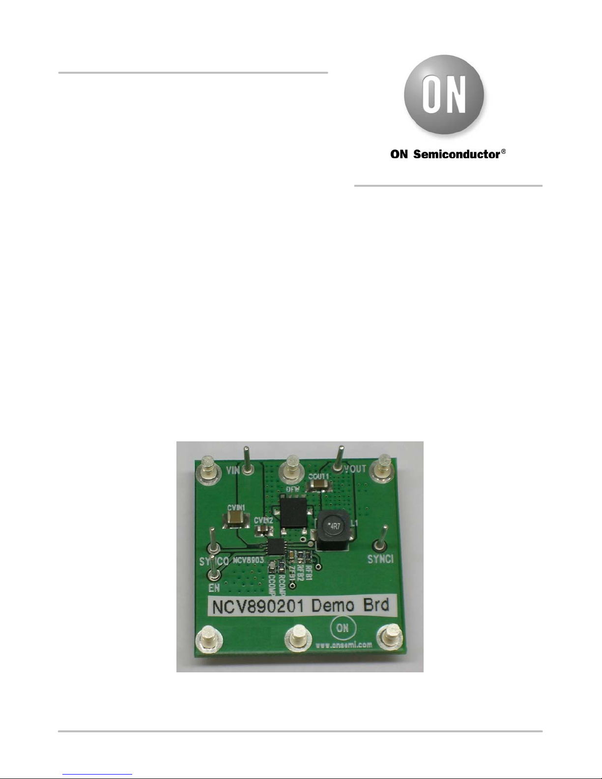
The NCV890201 demonstration board provides a convenient way to
evaluate a high-frequency buck converter design. No additional
components are required, other than dc supplies for the input and
enable voltages. An external clock can be used to synchronize the
switching frequency; and the board also provides a synchronization
output, enabling it to be used as a master. It is configured for a 3.3 V
output with a 2 MHz switching frequency and a 2.0 A maximum
output current, over the typical 4.5 V to 18 V automotive input voltage
range. In addition, the board regulates up to 36 V thanks to switching
frequency foldback.
Key Features
• 3.3 V Output Voltage
• 2 MHz Switching Frequency
• 2.0 A Current Limit
• Wide Input Voltage of 4.5 V to 36 V
• Regulates through Load Dump Conditions
• External Clock Synchronization up to 2.5 MHz
• Synchronization Output
• Automotive Grade
Figure 1. NCV890201GEVB Board Picture
http://onsemi.com
EVAL BOARD USER’S MANUAL
NCV890201GEVB
http://onsemi.com
2
Table 1. DEMONSTRATION BOARD TERMINALS
Terminal Function
VIN Positive dc input voltage
GND Common dc return
VOUT Regulated dc output voltage
EN Enable input
SYNCI Input for external clock synchronization
SYNCO Output for synchronizing other boards
Table 2. ABSOLUTE MAXIMUM RATINGS
(Voltages are with respect to GND)
Rating
Value Units
Dc supply voltage (VIN, EN) -0.3 to 36 V V
Dc supply voltage (SYNCI) -0.3 to 6 V V
Junction Temperature (NCV890201) -40 to 150 °C
Ambient temperature (Demo Board) -40 to 85 °C
Stresses exceeding Maximum Ratings may damage the device. Maximum Ratings are stress ratings only. Functional operation
above the Recommended Operating Conditions is not implied. Extended exposure to stresses above the Recommended
Operating Conditions may affect device reliability.
Table 3. ELECTRICAL CHARACTERISTICS
(TA = 25°C, 4.5 V ≤ VIN ≤ 40 V, VEN = 2 V, V
OUT
= 3.3 V, 0 ≤ I
OUT
≤ 2.0 A, unless otherwise specified)
Characteristics
Conditions Typical Value Units
Regulation
Output Voltage 3.30 V
Voltage Accuracy 4 %
Line Regulation I
OUT
= 1.0 A 0.12 %
Load Regulation VIN = 13.2 V 0.03 %
Switching
Switching Frequency 2.0 MHz
Soft-start Time 1.4 ms
SYNCI Frequency range 1.8 to 2.5 MHz
Current Limit
Average Current Limit VIN = 6 to 18 V 1.8 A
Cycle-by-cycle Current Limit 2.45 A
Protections
Input Undervoltage Lockout (UVLO) VIN decreasing 4.2 V
Thermal Shutdown TA increasing 170 °C

NCV890201GEVB
http://onsemi.com
3
Figure 2. NCV890201GEVB Board Schematic
Operational Guidelines
1. Connect a dc input voltage, within the 4.5 V to 36 V range, between VIN and GND
2. Connect a load between VOUT and GND
3. Connect a dc enable voltage, within the 4.5 V to 36 V range, between EN and GND
4. Optionally, for external clock synchronization, connect a pulse source between SYNCI and GND. The high state level
should be within the 2 to 6 V range, and the low state level within the -0.3 V to 0.8 V range, with a minimum pulse
width of 40 ns and a frequency within the 1.8 to 2.5 MHz range.
Figure 3. NCV890201GEVB Board Connections
V
IN
V
EN
Z
OUT
V
SYNCI
I
OUT
 Loading...