

Page 1
NCV8775C
f
Ultra Low Iq 350 mA LDO
Regulator with Reset
The NCV8775C is 350 mA LDO regulator with integrated reset
functions dedicated for microprocessor applications. Its robustness allows
NCV8775C to be used in severe automotive environments. Ultra low
quiescent current as low as 19 mA typical makes it suitable for
applications permanently connected to battery requiring ultra low
quiescent current with or without load. This feature is especially critical
when modules remain in active mode when ignition is off. The
NCV8775C contains protection functions as current limit, thermal
shutdown.
www.onsemi.com
MARKING
DIAGRAMS
Features
• Output Voltage Options: 3.3 V and 5 V
• Output Voltage Accuracy: ±2%
• Output Current up to 350 mA
• Ultra Low Quiescent Current: typ 19 mA (max 28 mA)
• Very Wide Range of C
and ESR Values for Stability
out
• Microprocessor Compatible Control Functions:
− Reset with Adjustable Delay
• Wide Input Voltage Operation Range: up to 40 V
• Protection Features
− Current Limitation
− Thermal Shutdown
• NCV Prefix for Automotive and Other Applications Requiring
Unique Site and Control Change Requirements; AEC−Q100 Grade 1
Qualified and PPAP Capable
• EMC Compliant
• These are Pb−Free Devices
Typical Applications
• Body Control Module
• Instruments and Clusters
• Occupant Protection and Comfort
• Powertrain
DPAK−5
DT SUFFIX
CASE 175AA
D2PAK−5
D5S SUFFIX
CASE 936A
xx = 50 (5.0 V Version)
= 33 (3.3 V Version)
A = Assembly Location
WL, L = Wafer Lot
Y = Year
WW = Work Week
G or G = Pb−Free Package
ORDERING INFORMATION
See detailed ordering and shipping information on page 12 o
this data sheet.
775CxxG
ALYWW
NC
V8775Cxx
AWLYWWG
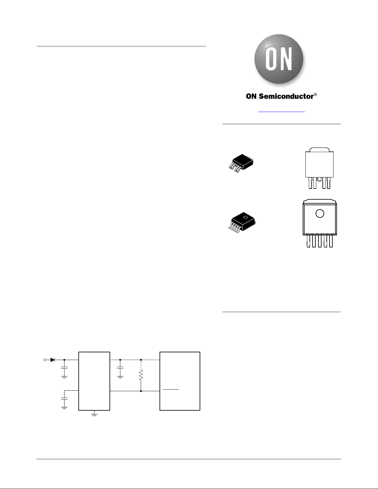
V
BAT
0.1 mF
C
D
47 nF
Figure 1. Typical Application Schematic
© Semiconductor Components Industries, LLC, 2017
December, 2019 − Rev. 1
C
in
V
in
NCV8775C
D
GND
V
out
RO
V
out
C
out
10 mF
R
RO
5 kW
V
DD
Microprocessor
RESET
1 Publication Order Number:
NCV8775C/D
Page 2
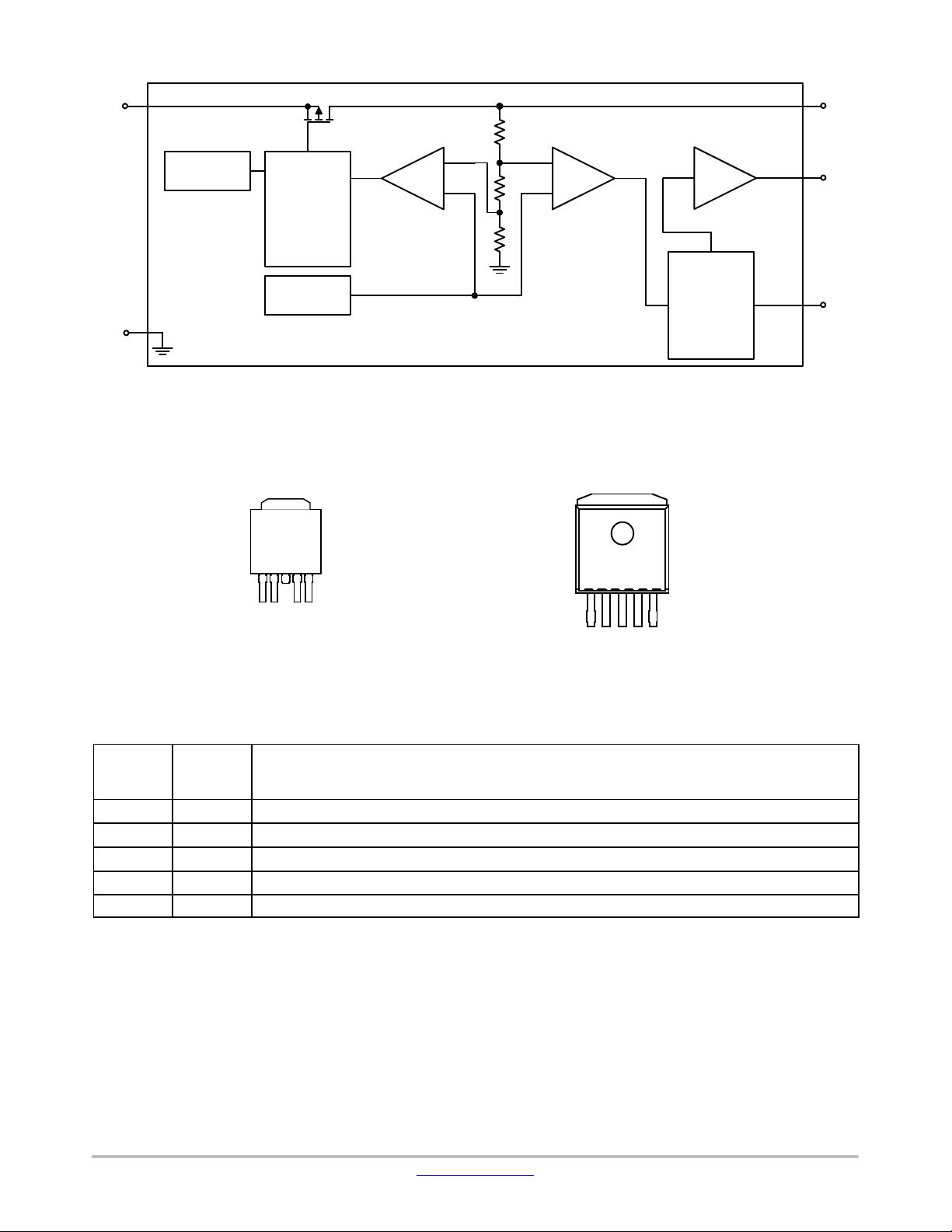
NCV8775C
PIN FUNCTION DESCRIPTION
Pin No.
Pin Name
Description
1
V
Positive Power Supply Input. Connect 0.1 mF capacitor to ground.
2ROReset (Open Collector) Output. External Pull−up resistor connected to V
.
3, TAB
GND
Power Supply Ground. Pin 3 internally connected to tab.
4DReset Delay. Timing capacitor to GND for Reset Delay function.
5
V
Regulated Output Voltage. Connect 10 mF capacitor with ESR < 5 W to ground.
V
GND
in
Thermal
Shutdown
V
RO
out
Driver
With
Current
Error Amplifier
Reset Comparator
Reset Driver
Limit
Reference
Delay
D
Timer
Figure 2. Simplified Block Diagram
PIN CONNECTIONS
PIN 1.V
in
2.RO
Tab, 3.GND
4.D
5.V
out
PIN 1.V
in
2.RO
Tab, 3.GND
4.D
5.V
out
DPAK−5
D2PAK−5
out
1
1
DPAK−5
D2PAK−5
Figure 3. Pin Connections
in
out
www.onsemi.com
2
Page 3
NCV8775C
ABSOLUTE MAXIMUM RATINGS
Rating
Symbol
Min
Max
Unit
Input Voltage (Note 1) DC
Vin−0.3
40
V
Input Voltage (Note 2) Load Dump − Suppressed
Us*−45
V
Output Voltage
V
−0.3
7
V
Reset Delay Voltage
VD−0.3
7
V
Reset Output Voltage
VRO−0.3
7
V
Junction Temperature
TJ−40
150
C
Storage Temperature
T
−55
150
C
ESD CAPABILITY (Note 3)
Rating
Symbol
Min
Max
Unit
ESD Capability, Human Body Model
ESD
−4
4
kV
ESD Capability, Charged Device Model
ESD
−1
1
kV
LEAD SOLDERING TEMPERATURE AND MSL (Note 4)
Rating
Symbol
Min
Max
Unit
Moisture Sensitivity Level DPAK−5
MSL
1
−
THERMAL CHARACTERISTICS (Note 5)
Rating
Symbol
Value
Unit
Thermal Characteristics, DPAK−5
C/W
Thermal Characteristics, D2PAK−5
C/W
RECOMMENDED OPERATING RANGE (Note 8)
Rating
Symbol
Min
Max
Unit
Input Voltage (Note 9)
Vin4.5
40
V
Junction Temperature
TJ−40
150
C
out
°
STG
Stresses exceeding those listed in the Maximum Ratings table may damage the device. If any of these limits are exceeded, device functionality
should not be assumed, damage may occur and reliability may be affected.
1. Refer to ELECTRICAL CHARACTERISTICS and APPLICATION INFORMATION for Safe Operating Area.
2. Load Dump Test B (with centralized load dump suppression) according to ISO16750−2 standard. Guaranteed by design. Not tested in
production. Passed Class A according to ISO16750−1.
HBM
CDM
3. This device series incorporates ESD protection and is tested by the following methods:
ESD HBM tested per AEC−Q100−002 (JS−001−2017)
Field Induced Charge Device Model ESD characterization is not performed on plastic molded packages with body sizes 2 x 2 mm due to
the inability of a small package body to acquire and retain enough charge to meet the minimum CDM discharge current waveform
characteristic defined in JEDEC JS−002−2018.
°
D2PAK−5
1
4. For more information, please refer to our Soldering and Mounting Techniques Reference Manual, SOLDERRM/D.
°
Thermal Resistance, Junction−to−Air (Note 6)
Thermal Reference, Junction−to−Lead (Note 6)
Thermal Resistance, Junction−to−Air (Note 7)
Thermal Reference, Junction−to−Lead (Note 7)
R
R
R
R
θJA
ψJL1
θJA
ψJL1
53.5
8.2
23.9
7.4
°
Thermal Resistance, Junction−to−Air (Note 6)
Thermal Reference, Junction−to−Lead (Note 6)
Thermal Resistance, Junction−to−Air (Note 7)
Thermal Reference, Junction−to−Lead (Note 7)
R
R
R
R
θJA
ψJL1
θJA
ψJL1
53.3
7.6
23.7
6.9
5. Refer to ELECTRICAL CHARACTERISTICS and APPLICATION INFORMATION for Safe Operating Area.
6. Values based on 1s0p board with copper area of 645 mm2 (or 1 in2) of 1 oz copper thickness and FR4 PCB substrate. Single layer − according
to JEDEC51.3.
7. Values based on 2s2p board with copper area of 645 mm2 (or 1 in2) of 1 oz copper thickness for inner layers, 2 oz copper thickness for signal
layers and FR4 PCB substrate. 4 layers − according to JEDEC51.7.
°
8. Refer to ELECTRICAL CHARACTERISTICS and APPLICATION INFORMATION for Safe Operating Area.
9. Minimum Vin = 4.5 V or (V
+ VDO), whichever is higher.
out
www.onsemi.com
3
Page 4
NCV8775C
ELECTRICAL CHARACTERISTICS V
= 13.5 V, Cin = 0.1 mF, C
= 10 mF, Min and Max values are valid for temperature range
Parameter
Test Conditions
Symbol
Min
Typ
Max
Unit
REGULATOR OUTPUT
Output Voltage (Accuracy %)
V
V
A
V
V
Line Regulation
V
V
Reg
−20020
mV
Load Regulation
I
= 0.1 mA to 350 mA
Reg
−351035
mV
Dropout Voltage (Note 12)
V
mV
QUIESCENT CURRENT
Quiescent Current (Iq = Iin − I
)
I
A
CURRENT LIMIT PROTECTION
Current Limit
V
= 0.96 x V
I
500−1100
mA
Short Circuit Current Limit
V
= 0 V
ISC500−1100
mA
PSRR
Power Supply Ripple Rejection (Note 13)
f = 100 Hz, 0.5 V
PSRR−80−dB
D (RESET DELAY)
Reset Charging Current
VD = 1.0 V
ID2.0
4.0
6.5
A
Upper Timing Threshold
VDU1.2
1.3
1.4
V
Reset Delay Time
CD = 47 nF
tRD101622
ms
Reset Reaction Time
tRR6.0
s
RESET OUTPUT RO
Input Voltage Reset Threshold
V
Vin decreasing, V
> V
V
V
Output Voltage Reset Threshold
V
decreasing
VRT909396
%V
Reset Hysteresis
VRH−
2.0−%V
Reset Output Low Voltage
V
> 1 V, RRO > 5 k
V
−
0.2
0.4
V
Reset High Level Leakage Current
I
−−5
A
THERMAL SHUTDOWN
Thermal Shutdown Temperature
TSD150
175
195°C
Thermal Shutdown Hysteresis
TSH−10−°C
Product parametric performance is indicated in the Electrical Characteristics for the listed test conditions, unless otherwise noted. Product per-
ty
in
out
−40°C ≤ TJ ≤ 150°C unless noted otherwise and are guaranteed by test, design or statistical correlation. Typical values are referenced to
T
= 25°C (Notes 10 and 11)
J
out
DO
LIM
line
load
q
3.234
3.234
4.9
4.9
−
−
−
−
3.3
3.3
5.0
5.0
200
350
19
−
3.366
3.366
5.1
5.1
350
600
m
27
28
out
3.3
Vin = 4.5 V to 40 V, I
= 4.5 V to 16 V, I
V
in
V
5.0
3.3
5.0
5.0 VI
= 5.6 V to 40 V, I
in
V
= 5.975 V to 16 V, I
in
Vin = 4.5 V to 28 V, I
Vin = 6 V to 28 V, I
out
= 200 mA
out
I
= 350 mA
out
I
= 0.1 mA, TJ = 25°C
out
I
= 0.1 mA, TJ ≤ 125°C
out
out
out
= 0.1 mA to 200 mA
out
= 0.1 mA to 350 mA
out
= 0.1 mA to 200 mA
out
out
= 5 mA
out
= 5 mA
out
out_nom
= 0.1 mA to 350 m
pp
out
3.3
out
out
RT
W
in_RT
ROL
ROLK
− 3.8 4.2
(Note 13)
(Note 13)
formance may not be indicated by the Electrical Characteristics if operated under different conditions.
10.Refer to ABSOLUTE MAXIMUM RATINGS and APPLICATION INFORMATION for Safe Operating Area.
11.Performance guaranteed over the indicated operating temperature range by design and/or characterization tested at T
cycle pulse techniques are used during testing to maintain the junction temperature as close to ambient as possible.
12.Measured when output voltage falls 100 mV below the regulated voltage at V
13.Values based on design and/or characterization.
= 13.5 V.
in
[ TJ. Low du
A
m
m
out
out
m
www.onsemi.com
4
Page 5
NCV8775C
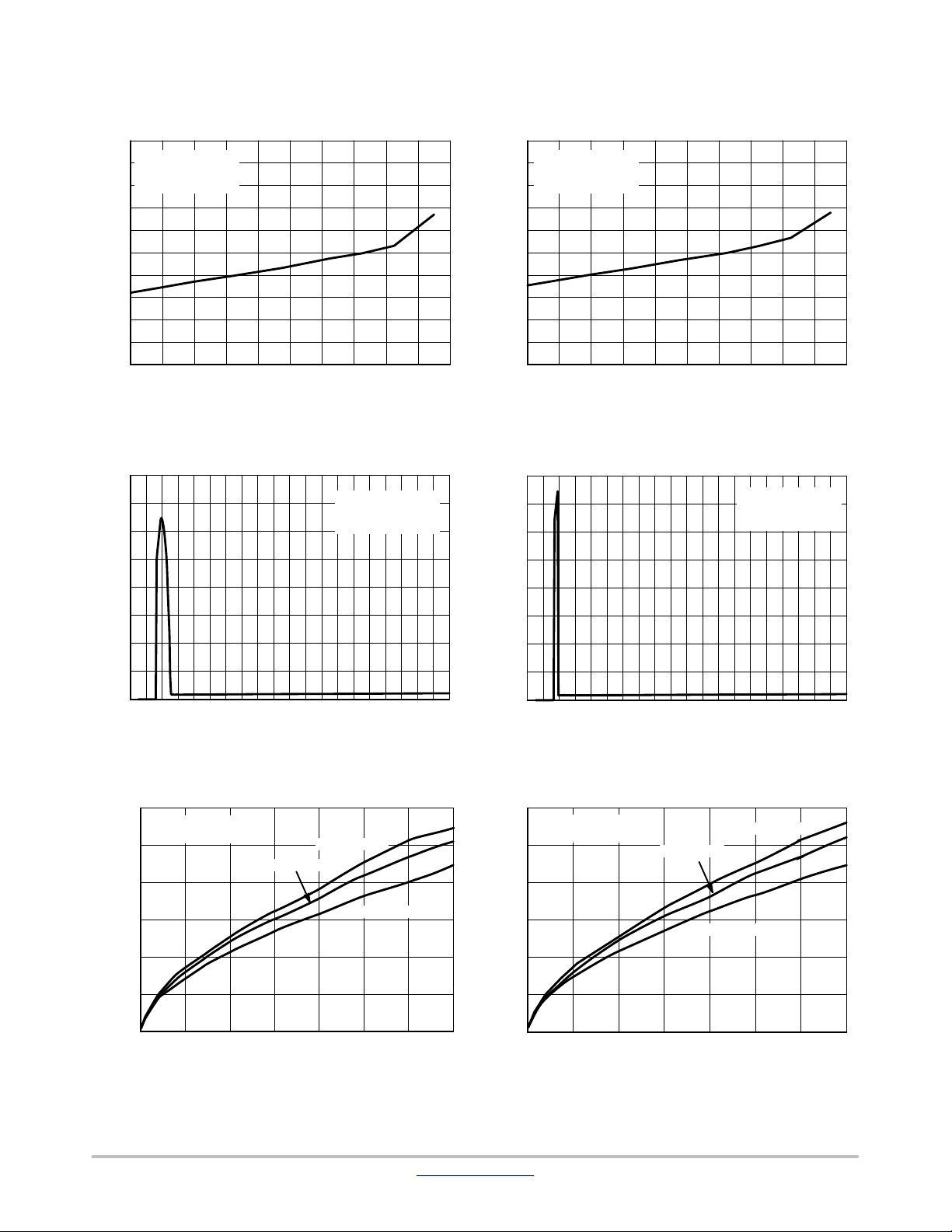
TYPICAL CHARACTERISTICS
30
Vin = 13.5 V
28
I
= 100 mA
out
26
V
out(nom)
= 5.0 V
24
22
20
18
16
14
, QUIESCENT CURRENT (mA)
q
I
12
10
−40 −20 0 20 40 60 80 100 120 140 160
TJ, JUNCTION TEMPERATURE (°C)
Figure 4. Quiescent Current vs. Junction
Temperature
800
I
= 100 mA
700
600
500
400
out
= 25°C
T
J
V
out(nom)
= 5.0 V
30
Vin = 13.5 V
28
I
= 100 mA
out
26
V
out(nom)
= 3.3 V
24
22
20
18
16
14
, QUIESCENT CURRENT (mA)
q
I
12
10
−40 −20 0 20 40 60 80 100 120 140 160
TJ, JUNCTION TEMPERATURE (°C)
Figure 5. Quiescent Current vs. Junction
Temperature
800
I
= 100 mA
700
600
500
400
out
= 25°C
T
J
V
out(nom)
= 3.3 V
, QUIESCENT CURRENT (mA)
q
I
300
200
100
0
300
200
, QUIESCENT CURRENT (mA)
100
q
I
0
0 4 8 12 16 20 24 28 32 36 40 0 4 8 12 16 20 24 28 32 36 40
Vin, INPUT VOLTAGE (V)
Figure 6. Quiescent Current vs. Input Voltage
1200
1000
Vin = 13.5 V
out(nom)
= 5.0 V
V
TJ = −40°C
Figure 7. Quiescent Current vs. Input Voltage
1200
1000
Vin = 13.5 V
V
out(nom)
Vin, INPUT VOLTAGE (V)
= 3.3 V
TJ = 25°C
TJ = −40°C
TJ = 25°C
800
600
TJ = 150°C
800
600
TJ = 150°C
400
200
, QUIESCENT CURRENT (mA)
q
I
0
0 50 100 150 200 250 300 350
I
, OUTPUT CURRENT (mA)
OUT
Figure 8. Quiescent Current vs. Output Current
400
200
, QUIESCENT CURRENT (mA)
q
I
0
0 50 100 150 200 250 300 350
I
, OUTPUT CURRENT (mA)
out
Figure 9. Quiescent Current vs. Output Current
www.onsemi.com
5
Page 6

NCV8775C
TYPICAL CHARACTERISTICS
5.10
Vin = 13.5 V
5.08
I
= 100 mA
out
5.06
V
out(nom)
= 5.0 V
5.04
5.02
5.00
4.98
4.96
, OUTPUT VOLTAGE (V)
4.94
out
V
4.92
4.90
−40 −20 0 20 40 60 80 100 120 140 160
TJ, JUNCTION TEMPERATURE (°C)
Figure 10. Output Voltage vs. Junction
Temperature
6
I
= 100 mA
out
out(nom)
= 5.0 V
V
5
4
3.38
Vin = 13.5 V
3.36
I
= 100 mA
out
3.34
V
out(nom)
= 3.3 V
3.32
3.30
3.28
3.26
, OUTPUT VOLTAGE (V)
out
V
3.24
3.22
−40 −20 0 20 40 60 80 100 120 140 160
TJ, JUNCTION TEMPERATURE (°C)
Figure 11. Output Voltage vs. Junction
Temperature
4
I
= 100 mA
out
out(nom)
= 3.3 V
3.5
2.5
V
3
3
2
, OUTPUT VOLTAGE (V)
out
1
V
0
012345678
TJ = 25°C
TJ = −40°C
TJ = 150°C
Vin, INPUT VOLTAGE (V)
Figure 12. Output Voltage vs. Input Voltage
700
Vin = 13.5 V
out(nom)
= 5.0 V
600
V
500
400
TJ = 25°C
300
TJ = 150°C
200
, DROPOUT VOLTAGE (mV)
100
DO
V
TJ = −40°C
0
0 50 100 150 200 250 300 350
I
, OUTPUT CURRENT (mA)
out
Figure 14. Dropout Voltage vs. Output Current
2
1.5
1
, OUTPUT VOLTAGE (V)
out
V
0.5
TJ = 25°C
TJ = −40°C
TJ = 150°C
0
012345678
Vin, INPUT VOLTAGE (V)
Figure 13. Output Voltage vs. Input Voltage
700
Vin = 13.5 V
out(nom)
= 5.0 V
I
= 350 mA
out
600
500
V
400
300
I
= 200 mA
out
200
, DROPOUT VOLTAGE (mV)
100
DO
V
0
−40 160140−20 0 20406080 120100
TJ, JUNCTION TEMPERATURE (°C)
Figure 15. Dropout Voltage vs. Junction
Temperature
www.onsemi.com
6
Page 7

NCV8775C
TYPICAL CHARACTERISTICS
1000
800
600
ISC @ V
I
LIM
out
@ V
= 0 V
out
= 4.8 V
400
, CURRENT LIMIT (mA)
SC
I
200
LIM
I
0
0 5 10 15 20 25 30 35 40
TJ = 25°C
V
out(nom)
= 5.0 V
Vin, INPUT VOLTAGE (V)
Figure 16. Output Current Limit vs. Input
Voltage
1100
1000
900
800
700
Vin = 13.5 V
V
out(nom)
= 5.0 V
ISC @ V
I
@ V
LIM
out
out
= 0 V
= 4.8 V
1000
ISC @ V
out
= 0 V
800
I
@ V
LIM
= 3.168 V
out
600
400
, CURRENT LIMIT (mA)
SC
I
200
LIM
I
0
0 5 10 15 20 25 30 35 40
TJ = 25°C
V
out(nom)
Vin, INPUT VOLTAGE (V)
Figure 17. Output Current Limit vs. Input
Voltage
1100
1000
900
800
700
Vin = 13.5 V
out(nom)
= 3.3 V
V
ISC @ V
I
@ V
LIM
= 0 V
out
= 3.168 V
out
= 3.3 V
, CURRENT LIMIT (mA)
600
SC
I
500
LIM
I
400
−40 −20 0 20 40 60 80 100 120 140 160
TJ, JUNCTION TEMPERATURE (°C)
Figure 18. Output Current Limit vs. Junction
Temperature
100
10
Unstable Region
Stable Region
1
ESR (W)
0.1
Vin = 13.5 V
out(nom)
= 5.0 V
0.01
V
Cout = 1.0 mF − 100 mF
0 50 100 150 200 250 300 350
I
, OUTPUT CURRENT (mA)
out
Figure 20. Output Stability with Output
Capacitor ESR
, CURRENT LIMIT (mA)
600
SC
I
500
LIM
I
400
−40 −20 0 20 40 60 80 100 120 140 160
TJ, JUNCTION TEMPERATURE (°C)
Figure 19. Output Current Limit vs. Junction
Temperature
100
10
Unstable Region
Stable Region
1
ESR (W)
0.1
0.01
Vin = 13.5 V
out(nom)
= 3.3 V
V
Cout = 1.0 mF − 100 mF
0 50 100 150 200 250 300 350
I
, OUTPUT CURRENT (mA)
out
Figure 21. Output Stability with Output
Capacitor ESR
www.onsemi.com
7
Page 8

NCV8775C
TYPICAL CHARACTERISTICS
4.8
4.75
Vin = 13.5 V
out(nom)
= 5.0 V
V
4.7
4.65
4.6
, RESET THRESHOLD (V)
4.55
RT
V
4.5
−40 −20 0 20 40 60 80 100 120 140 160
TJ, JUNCTION TEMPERATURE (°C)
Figure 22. Reset Threshold vs. Junction
Temperature
4.2
4.1
4.0
3.9
Vin = 13.5 V
V
out(nom)
= 3.3 V
3.17
Vin = 13.5 V
V
out(nom)
3.13
3.09
3.05
, RESET THRESHOLD (V)
3.01
RT
V
2.97
−40 −20 0 20 40 60 80 100 120 140 160
TJ, JUNCTION TEMPERATURE (°C)
Figure 23. Reset Threshold vs. Junction
Temperature
= 3.3 V
3.8
3.7
THRESHOLD (V)
, INPUT VOLTAGE RESET
3.6
RT
_
in
3.5
V
3.4
−40 −20 0 20 40 60 80 100 120 140 160
TJ, JUNCTION TEMPERATURE (°C)
Figure 24. Input Voltage Reset Threshold vs.
Junction Temperature
22
20
18
16
14
, RESET DELAY TIME (ms)
12
RD
t
10
−40 −20 0 20 40 60 80 100 120 140 160
TJ, JUNCTION TEMPERATURE (°C)
Vin = 13.5 V
= 47 nF
C
D
V
out(nom)
= 5.0 V
Figure 25. Reset Delay Time vs. Junction
Temperature
22
Vin = 13.5 V
= 47 nF
C
20
D
V
out(nom)
= 3.3 V
18
16
14
, RESET DELAY TIME (ms)
12
RD
t
10
−40 −20 0 20 40 60 80 100 120 140 160
TJ, JUNCTION TEMPERATURE (°C)
Figure 26. Reset Delay Time vs. Junction
Temperature
www.onsemi.com
8
Page 9

TYPICAL CHARACTERISTICS
PSRR (dB)
120
0
100
I
= 100 mA
80
60
40
Vin = 13.5 V ± 0.5 V
20
0
C
out
V
out(nom)
= 1 mF
= 5.0 V
PP
10 100 1000 10000 100000 1000000
f, FREQUENCY (Hz)
Figure 27. PSRR vs. Frequency
out
I
= 100 mA
out
NCV8775C
6000
5500
5000
4500
4000
3500
3000
2500
2000
1500
NOISE DENSITY (nV/√Hz)
1000
500
0
f = 10 Hz − 100 kHz
V
= 268 mV
n
Vin = 13.5 V
C
= 1 mF
out
I
= 100 mA
out
V
out(nom)
= 5.0 V
10 100 1000 10000 10000
f, FREQUENCY (Hz)
Figure 28. Noise vs. Frequency
V
in
(10 V/div)
V
out
(20 mV/div)
V
in
(5 V/div)
V
out
(5 V/div)
V
RO
(5 V/div)
0 V
28 V
6 V
TJ = 25°C
I
= 100 mA
out
C
= 10 mF
out
t
= 1 ms (Vin)
rise/fall
I
out
(200 mA/div)
350 mA
5.17 V
5.012 V
out
(200 mV/div)
5 V
V
4.78 V
5 V
TIME (400 ms/div)
4.995 V
TIME (100 ms/div)
Figure 29. Line Transients Figure 30. Load Transients
TJ = 25°C
= 100 mA
I
13.5 V
0 V
0 V
out
C
out
C
= 47 nF
D
t
rise/fall
= 10 mF
= 1 s (Vin)
TJ = 25°C
= 13.5 V
V
in
C
= 10 mF
out
t
= 1 ms (I
rise/fall
0.1 mA
out
)
TIME (400 ms/div)
Figure 31. Power Up/Down Response
www.onsemi.com
9
Page 10
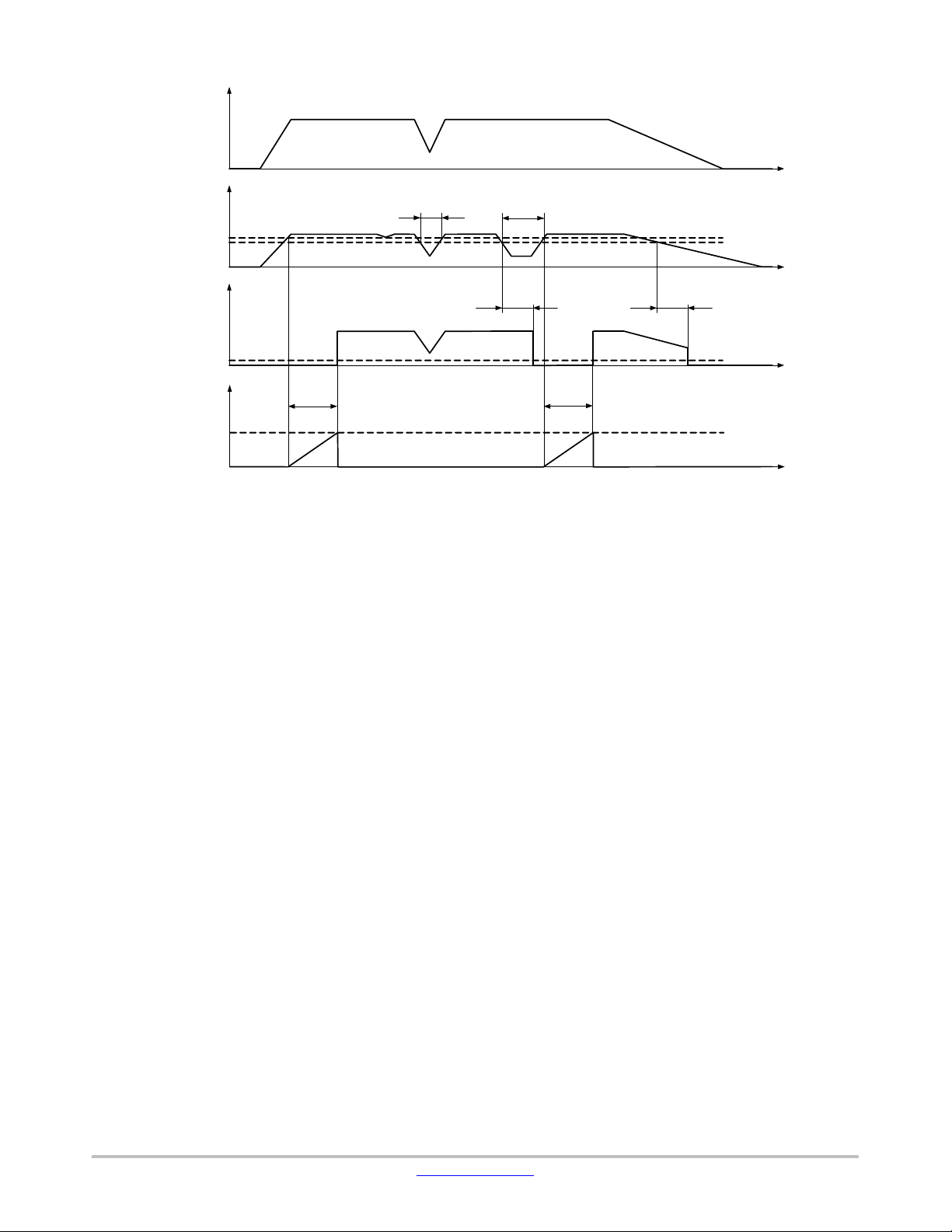
NCV8775C
V
in
V
out
VRT+ V
RH
V
RT
V
RO
V
ROL
V
D
V
DU
t
RD
Figure 32. Reset Function and Timing Diagram
DEFINITIONS
General
All measurements are performed using short pulse low
duty cycle techniques to maintain junction temperature as
close as possible to ambient temperature.
Output voltage
The output voltage parameter is defined for specific
temperature, input voltage and output current values or
specified over Line, Load and Temperature ranges.
Line Regulation
The change in output voltage for a change in input voltage
measured for specific output current over operating ambient
temperature range.
Load Regulation
The change in output voltage for a change in output
current measured for specific input voltage over operating
ambient temperature range.
Dropout Voltage
The input to output differential at which the regulator
output no longer maintains regulation against further
reductions in input voltage. It is measured when the output
drops 100 mV below its nominal value. The junction
temperature, load current, and minimum input supply
requirements affect the dropout level.
Quiescent Current
Quiescent Current (Iq) is the difference between the input
current (measured through the LDO input pin) and the
output load current.
t
>t
RR
RR
t
RR
t
RD
< t
RR
Current Limit and Short Circuit Current Limit
Current Limit is value of output current by which output
voltage drops below 96% of its nominal value. Short Circuit
Current Limit is output current value measured with output
of the regulator shorted to ground.
PSRR
Power Supply Rejection Ratio is defined as ratio of output
voltage and input voltage ripple. It is measured in decibels
(dB).
Line Transient Response
Typical output voltage overshoot and undershoot
response when the input voltage is excited with a given
slope.
Load Transient Response
Typical output voltage overshoot and undershoot
response when the output current is excited with a given
slope between low−load and high−load conditions.
Thermal Protection
Internal thermal shutdown circuitry is provided to protect
the integrated circuit in the event that the maximum junction
temperature is exceeded. When activated at typically 175°C,
the regulator turns off. This feature is provided to prevent
failures from accidental overheating.
Maximum Package Power Dissipation
The power dissipation level is maximum allowed power
dissipation for particular package or power dissipation at
which the junction temperature reaches its maximum
operating value, whichever is lower.
t
t
t
t
www.onsemi.com
10
Page 11

NCV8775C
APPLICATIONS INFORMATION
The NCV8775C regulator is self−protected with internal
thermal shutdown and internal current limit. Typical
characteristics are shown in Figure 4 to Figure 34.
Input Decoupling (Cin)
A ceramic or tantalum 0.1 mF capacitor is recommended
and should be connected close to the NCV8775C package.
Higher capacitance and lower ESR will improve the overall
line and load transient response.
Input Capacitor is required if regulator is located far from
power supply filter . If extremely fast input voltage transients
are expected with slew rate in excess of 4 V/ms then
appropriate input filter must be used. The filter can be
composed of several capacitors in parallel.
Output Decoupling (C
out
)
The NCV8775C is a stable component and does not
require a minimum Equivalent Series Resistance (ESR) for
the output capacitor. Stability region of ESR vs Output
Current is shown in Figures 20 and 21. The minimum output
decoupling value is 1 mF and can be augmented to fulfill
stringent load transient requirements. The regulator works
with ceramic chip capacitors as well as tantalum devices.
Larger values improve noise rejection and load regulation
transient response.
Reset Operation
A reset signal is provided on the Reset Output (RO) pin to
provide feedback to the microprocessor of an out of
regulation condition. The timing diagram of reset function
is shown in Figure 32. This is in the form of a logic signal on
RO. Output voltage conditions below the Reset threshold
cause RO to go low. RO is pulled up to V
by an external
out
resistor, typically 5.0 kW in value. Output voltage regulation
must be maintained for the delay time before the reset output
signals a valid condition. The delay for the reset output is
defined as the amount of time it takes the timing capacitor
on the delay pin to charge from a residual voltage of 0 V to
the upper timing threshold voltage V
charging current for this is I
of 4 mA and D pin voltage in
D
of 1.3 V. The
DU
steady state is typically 0 V. By using typical IC parameters
with a 47 n F capacitor on the D Pin, the following time delay
is derived:
V
tRD+ C
tRD+ 47 nF
DU
D
I
D
1.3 V
4 mA
+ 15.3 ms
(eq. 1)
Other time delays can be obtained by changing the C
capacitor value. The Delay Time can be reduced by
decreasing the ca p acitance of C
. Using the formula above,
D
Delay can be reduced as desired. For minimum reset delay
time Delay pin must be left open with no PCB trace
connected to the pin.
Thermal Considerations
As power in the NCV8775C increases, it might become
necessary to provide some thermal relief. The maximum
power dissipation supported by the device is dependent
upon board design and layout. Mounting pad configuration
on the PCB, the board material, and the ambient temperature
affect the rate of junction temperature rise for the part. When
the NCV8775C has good thermal conductivity through the
PCB, the junction temperature will be relatively low with
high power applications. The maximum dissipation the
NCV8775C can handle is given by:
P
D(max
ƪ
T
J(max)
+
)
R
qJA
* T
ƫ
A
(eq. 2)
Since TJ is not recommended to exceed 150°C, then the
NCV8775C soldered on 645 mm
2
, 1 oz copper area, FR4
can dissipate up to 2.35 W (for D2PAK−5) when the ambient
temperature (T
) is 25°C. See Figures 33 and 34 for R
A
JA
q
versus PCB area. The power dissipated by the NCV8775C
can be calculated from the following equations:
PD+ V
in
ǒ
Iq@I
out
Ǔ
) I
out
ǒ
Vin* V
out
Ǔ
(eq. 3)
or
V
NOTE: Items containing I
in(max)
+
P
D(max)
can be neglected if I
q
ǒ
)
V
out
I
) I
out
Ǔ
I
out
q
out
(eq. 4)
>> Iq.
D
www.onsemi.com
11
Page 12

NCV8775C
ORDERING INFORMATION
Device
Output Voltage
Package
Shipping
†
NCV8775CDT33RKG
3.3 V
DPAK−5
2500 / Tape & Reel
NCV8775CDT50RKG
5.0 V
DPAK−5
2500 / Tape & Reel
NCV8775CDS33R4G
3.3 V
D2PAK−5
800 / Tape & Reel
NCV8775CDS50R4G
5.0 V
D2PAK−5
800 / Tape & Reel
110
100
90
80
70
60
50
(°C/W)
40
30
, THERMAL RESISTANCE
20
JA
q
R
10
1 oz, Single Layer
2 oz, Single Layer
1 oz, 4 Layer
0
0 200 400 600 800 1000
COPPER HEAT SPREADER AREA (mm2)
Figure 33. Thermal Resistance vs. PCB Copper
Area (DPAK−5)
Hints
Vin and GND printed circuit board traces should be as
wide as possible. When the impedance of these traces is
high, there is a chance to pick up noise or cause the regulator
to malfunction. Place external filter components, especially
the output capacitor, as near as possible to the device to
increase EMC performance.
110
100
90
80
70
1 oz, Single Layer
2 oz, Single Layer
1 oz, 4 Layer
(°C/W)
, THERMAL RESISTANCE
JA
q
R
60
50
40
30
20
10
0
0 200 400 600 800 1000
COPPER HEAT SPREADER AREA (mm2)
Figure 34. Thermal Resistance vs. PCB Copper
Area (D2PAK−5)
The NCV8775C is not developed in compliance with
ISO26262 standard. If application is safety critical then the
above application example diagram shown in Figure 35 can
be used.
V
BAT
V
in
C
in
NCV8775C
C
D
D
GND
V
RO
V
out
out
C
out
V
CC
RESET
Voltage
Supervisor
(e.g. NCV30X, NCV809)
GND
V
DD
I/O
Microprocessor
I/O
Figure 35. NCV8775C Application Diagram
(Pb−Free)
(Pb−Free)
(Pb−Free)
†For information on tape and reel specifications, including part orientation and tape sizes, please refer to our Tape and Reel Packaging
Specifications Brochure, BRD8011/D.
(Pb−Free)
www.onsemi.com
12
Page 13

MECHANICAL CASE OUTLINE
PACKAGE DIMENSIONS
DPAK−5, CENTER LEAD CROP
SCALE 1:1
B
V
S
R
A
1234 5
K
F
L
D
5 PL
G
0.13 (0.005) T
RECOMMENDED
SOLDERING FOOTPRINT*
C
J
H
M
−T−
CASE 175AA
SEATING
PLANE
E
U
ISSUE B
R1
DATE 15 MAY 2014
NOTES:
1. DIMENSIONING AND TOLERANCING
PER ANSI Y14.5M, 1982.
2. CONTROLLING DIMENSION: INCH.
DIM MIN MAX MIN MAX
A 0.235 0.245 5.97 6.22
B 0.250 0.265 6.35 6.73
Z
C 0.086 0.094 2.19 2.38
D 0.020 0.028 0.51 0.71
E 0.018 0.023 0.46 0.58
F 0.024 0.032 0.61 0.81
G 0.180 BSC 4.56 BSC
H 0.034 0.040 0.87 1.01
J 0.018 0.023 0.46 0.58
K 0.102 0.114 2.60 2.89
L 0.045 BSC 1.14 BSC
R 0.170 0.190 4.32 4.83
R1 0.185 0.210 4.70 5.33
S 0.025 0.040 0.63 1.01
U 0.020 −−− 0.51 −−−
V 0.035 0.050 0.89 1.27
Z 0.155 0.170 3.93 4.32
MILLIMETERSINCHES
GENERIC
MARKING DIAGRAMS*
6.4
0.252
5.8
0.228
10.6
0.417
2.2
0.086
0.013
SCALE 4:1
0.34
0.8
0.031
ǒ
inches
5.36
0.217
mm
Ǔ
*For additional information on our Pb−Free strategy and soldering
details, please download the ON Semiconductor Soldering and
Mounting Techniques Reference Manual, SOLDERRM/D.
XXXXXXG
ALYWW
AYWW
XXX
XXXXXG
DiscreteIC
XXXXXX = Device Code
A = Assembly Location
L = Wafer Lot
Y = Year
WW = Work Week
G = Pb−Free Package
*This information is generic. Please refer to
device data sheet for actual part marking.
Pb−Free indicator, “G” or microdot “ G”,
may or may not be present.
DOCUMENT NUMBER:
DESCRIPTION:
ON Semiconductor and are trademarks of Semiconductor Components Industries, LLC dba ON Semiconductor or its subsidiaries in the United States and/or other countries.
ON Semiconductor reserves the right to make changes without further notice to any products herein. ON Semiconductor makes no warranty, representation or guarantee regarding
the suitability of its products for any particular purpose, nor does ON Semiconductor assume any liability arising out of the application or use of any product or circuit, and specifically
disclaims any and all liability, including without limitation special, consequential or incidental damages. ON Semiconductor does not convey any license under its patent rights nor the
rights of others.
© Semiconductor Components Industries, LLC, 2019
98AON12855D
DPAK−5 CENTER LEAD CROP
Electronic versions are uncontrolled except when accessed directly from the Document Repository.
Printed versions are uncontrolled except when stamped “CONTROLLED COPY” in red.
PAGE 1 OF 1
www.onsemi.com
Page 14

MECHANICAL CASE OUTLINE
PACKAGE DIMENSIONS
SCALE 1:1
G
S
H
OPTIONAL
CHAMFER
N
R
K
B
D
0.010 (0.254) T
M
C
A
123
45
SOLDERING FOOTPRINT
8.38
0.33
D2PAK 5−LEAD
CASE 936A−02
ISSUE D
−T−
E
M
L
1.702
0.067
TERMINAL 6
V
P
DATE 15 SEP 2015
NOTES:
1. DIMENSIONING AND TOLERANCING PER ANSI
Y14.5M, 1982.
2. CONTROLLING DIMENSION: INCH.
3. TAB CONTOUR OPTIONAL WITHIN DIMENSIONS A
U
AND K.
4. DIMENSIONS U AND V ESTABLISH A MINIMUM
MOUNTING SURFACE FOR TERMINAL 6.
5. DIMENSIONS A AND B DO NOT INCLUDE MOLD
FLASH OR GATE PROTRUSIONS. MOLD FLASH
AND GATE PROTRUSIONS NOT TO EXCEED 0.025
(0.635) MAXIMUM.
_
8
MILLIMETERS
_
0
8
_
DIMAMIN MAX MIN MAX
INCHES
0.386 0.403 9.804 10.236
B 0.356 0.368 9.042 9.347
C 0.170 0.180 4.318 4.572
D 0.026 0.036 0.660 0.914
E 0.045 0.055 1.143 1.397
G 0.067 BSC 1.702 BSC
H 0.539 0.579 13.691 14.707
K 0.050 REF 1.270 REF
L 0.000 0.010 0.000 0.254
M 0.088 0.102 2.235 2.591
N 0.018 0.026 0.457 0.660
P 0.058 0.078 1.473 1.981
_
R
0
S 0.116 REF 2.946 REF
U 0.200 MIN 5.080 MIN
V 0.250 MIN 6.350 MIN
GENERIC
MARKING DIAGRAM*
xx
xxxxxxxxx
AWLYWWG
10.66
0.42
xxxxxx = Device Code
A = Assembly Location
WL = Wafer Lot
Y = Year
WW = Work Week
G = Pb−Free Package
*This information is generic. Please refer to
device data sheet for actual part marking.
16.02
0.63
3.05
0.12
SCALE 3:1
ǒ
inches
1.016
mm
0.04
Ǔ
Pb−Free indicator, “G” or microdot “ G”,
may or may not be present.
DOCUMENT NUMBER:
DESCRIPTION:
ON Semiconductor and are trademarks of Semiconductor Components Industries, LLC dba ON Semiconductor or its subsidiaries in the United States and/or other countries.
ON Semiconductor reserves the right to make changes without further notice to any products herein. ON Semiconductor makes no warranty, representation or guarantee regarding
the suitability of its products for any particular purpose, nor does ON Semiconductor assume any liability arising out of the application or use of any product or circuit, and specifically
disclaims any and all liability, including without limitation special, consequential or incidental damages. ON Semiconductor does not convey any license under its patent rights nor the
rights of others.
98ASH01006A
D2PAK 5−LEAD
Electronic versions are uncontrolled except when accessed directly from the Document Repository.
Printed versions are uncontrolled except when stamped “CONTROLLED COPY” in red.
PAGE 1 OF 1
© Semiconductor Components Industries, LLC, 2019
www.onsemi.com
Page 15

ON Semiconductor and are trademarks of Semiconductor Components Industries, LLC dba ON Semiconductor or its subsidiaries in the United States and/or other countries.
ON Semiconductor owns the rights to a number of patents, trademarks, copyrights, trade secrets, and other intellectual property. A listing of ON Semiconductor’s product/patent
coverage may be accessed at www.onsemi.com/site/pdf/Patent−Marking.pdf
ON Semiconductor makes no warranty, representation or guarantee regarding the suitability of its products for any particular purpose, nor does ON Semiconductor assume any liability
arising out of the application or use of any product or circuit, and specifically disclaims any and all liability, including without limitation special, consequential or incidental damages.
Buyer is responsible for its products and applications using ON Semiconductor products, including compliance with all laws, regulations and safety requirements or standards,
regardless of any support or applications information provided by ON Semiconductor. “Typical” parameters which may be provided in ON Semiconductor data sheets and/or
specifications can and do vary in different applications and actual performance may vary over time. All operating parameters, including “Typicals” must be validated for each customer
application by customer’s technical experts. ON Semiconductor does not convey any license under its patent rights nor the rights of others. ON Semiconductor products are not
designed, intended, or authorized for use as a critical component in life support systems or any FDA Class 3 medical devices or medical devices with a same or similar classification
in a foreign jurisdiction or any devices intended for implantation in the human body. Should Buyer purchase or use ON Semiconductor products for any such unintended or unauthorized
application, Buyer shall indemnify and hold ON Semiconductor and its officers, employees, subsidiaries, affiliates, and distributors harmless against all claims, costs, damages, and
expenses, and reasonable attorney fees arising out of, directly or indirectly, any claim of personal injury or death associated with such unintended or unauthorized use, even if such
claim alleges that ON Semiconductor was negligent regarding the design or manufacture of the part. ON Semiconductor is an Equal Opportunity/Affirmative Action Employer. This
literature is subject to all applicable copyright laws and is not for resale in any manner.
. ON Semiconductor reserves the right to make changes without further notice to any products herein.
PUBLICATION ORDERING INFORMATION
LITERATURE FULFILLMENT:
Email Requests to: orderlit@onsemi.com
ON Semiconductor Website: www.onsemi.com
TECHNICAL SUPPORT
North American Technical Support:
Voice Mail: 1 800−282−9855 Toll Free USA/Canada
Phone: 011 421 33 790 2910
Europe, Middle East and Africa Technical Support:
Phone: 00421 33 790 2910
For additional information, please contact your local Sales Representative
◊
www.onsemi.com
1
 Loading...