

Page 1
查询NCV8184供应商
NCV8184
Micropower 70 mA
Low Dropout Tracking
Regulator/Line Driver
The NCV8184 is a monolithic integrated low dropout tracking
voltage regulator designed to provide an adjustable buffered output
voltage that closely tracks (±5.0 mV) the reference input.
The part can be used in automotive applications with remote
sensors, or any situation where it is necessary to isolate the output of
your regulator.
The NCV8184 also enables the user to bestow a quick upgrade to
their module when added current is needed, and the existing regulator
cannot provide.
The versatility of this part also enables it to be used as a high−side
driver.
Features
• 70 mA Source Capability
• Output Tracks within ±5.0 mV
• Low Input Voltage Tracking Performance
(Works Down to V
• Low Dropout (0.35 V Typ. @ 50 mA)
• Low Quiescent Current
• Thermal Shutdown
• Wide Operating Range
• Internally Fused Leads in SO−8 Package
• NCV Prefix, for Automotive and Other Applications Requiring Site
and Change Control
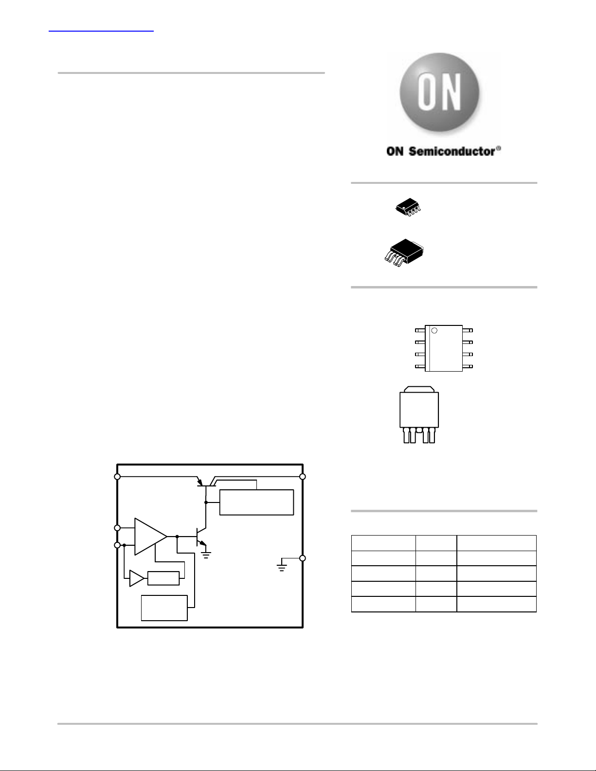
V
IN
REF
= 2.1 V)
Current Limit &
Saturation Sense
V
OUT
http://onsemi.com
8
1
1
5
D SUFFIX
CASE 751
DT SUFFIX
CASE 175AA
PIN CONNECTIONS AND
MARKING DIAGRAM
1
V
OUT
8184
ALYWW
1
A = Assembly Location
L = Wafer Lot
Y = Year
WW, W = Work Week
ALYW
8184
Pin 1. V
Tab, 3. GND
8
SO−8
DPAK
5−LEAD
V
IN
GNDGND
GNDGND
V
REF
IN
2. V
OUT
4. Adj
5. V
REF
/ENABLEAdj
/ENABLE
−
+
BIAS
Thermal
Shutdown
V
REF
Adj
/ENABLE
Figure 1. Block Diagram
Semiconductor Components Industries, LLC, 2004
August, 2004 − Rev. 15
ORDERING INFORMATION
Device Package Shipping
GND
1 Publication Order Number:
NCV8184D SO−8 95 Units/Rail
NCV8184DR2 SO−8
NCV8184DT DPAK
NCV8184DTRK DPAK 2500 Tape & Reel
†For information on tape and reel specifications,
including part orientation and tape sizes, please
refer to our Tape and Reel Packaging Specifications
Brochure, BRD8011/D.
2500 Tape & Reel
50 Units/Rail
†
NCV8184/D
Page 2
NCV8184
MAXIMUM RATINGS
Rating Value Unit
Storage Temperature −65 to 150 °C
Supply Voltage Range (continuous) −15 to 42 V
Supply Voltage Operating Range 4.0 to 42 V
Peak Transient Voltage (VIN = 14 V, Load Dump Transient = 28 V) 42 V
Voltage Range (V
Voltage Range (V
Maximum Junction Temperature 150 °C
ESD Capability Human Body Model
, Adj) −3.0 to 42 V
OUT
/ENABLE) −0.3 to 42 V
REF
2.5
Machine Model
200
kV
V
Lead Temperature Soldering: Reflow: (SMD styles only) (Note 1) 240 peak
°C
(Note 2)
Maximum ratings are those values beyond which device damage can occur. Maximum ratings applied to the device are individual stress limit
values (not normal operating conditions) and are not valid simultaneously . If these limits are exceeded, device functional operation is not implied,
damage may occur and reliability may be affected.
1. 60 second maximum above 183°C.
2. −5°C / +0°C Allowable Conditions
THERMAL CHARACTERISTICS
See Package Thermal Data Section (Page 8)
ELECTRICAL CHARACTERISTICS (V
= 1.0 mA; Adj = V
I
OUT
Parameter
Regular Output
V
/ENABLE − V
REF
V
Tracking Error
OUT
Dropout Voltage (VIN − V
Line Regulation 6.0 V ≤ VIN ≤ 26 V, V
Load Regulation 100 A ≤ I
Adj Input Bias Current V
Current Limit VIN = 14 V, V
Quiescent Current (IIN − I
Ripple Rejection f = 120 Hz, I
Thermal Shutdown Guaranteed by Design 150 180 210 °C
V
/ENABLE
REF
Enable Voltage − 0.8 − 2.1 V
Input Bias Current V
OUT
OUT
; C
OUT
OUT
OUT−ESR
= 1.0 , unless otherwise specified.)
6.0 V ≤ VIN ≤ 26 V, 100 A ≤ I
2.1 V ≤ V
V
= 12 V, I
IN
) I
OUT
I
OUT
I
OUT
REF
) VIN = 12 V, I
V
= 12 V, I
IN
V
= 12 V, V
IN
REF
= 14 V; V
IN
/ENABLE > 2.1 V; −40°C < TJ < +125°C; C
REF
= 1.0 F;
OUT
Test Conditions Min Typ Max Unit
/ENABLE ≤ (VIN − 600 mV)
REF
= 5.0 mA, V
OUT
= 100 A
= 5.0 mA
= 50 mA
REF
≤ 50 mA, V
OUT
≤ 50 mA
OUT
/ENABLE = 5.0 V
REF
/ENABLE = 5.0 V − − 10 mV
/ENABLE = 5.0 V − − 10 mV
REF
−10
−5.0
−
−
−
−
−
100
250
350
10
5.0
150
500
600
/ENABLE = 5.0 V − 0.2 1.0 A
/ENABLE = 5.0 V, V
REF
= 50 mA
OUT
= 100 A
OUT
/ENABLE = 0 V
REF
= 50 mA, 6.0 V ≤ VIN ≤ 26 V 60 − − dB
OUT
= 90% of Adj 70 − 400 mA
OUT
−
−
−
5.0
50
7.0
70
−
20
/ENABLE = 5.0 V − 0.2 1.0 A
mV
mV
mV
mV
mV
mA
A
A
http://onsemi.com
2
Page 3

PACKAGE PIN DESCRIPTION
Package Lead Number
SO−8 DPAK, 5−LEAD
8 1 V
1 2 V
2, 3, 6, 7 Tab, 3 GND Ground.
4 4 Adj Adjust lead, noninverting input.
5 5 V
Lead Symbol Function
IN
OUT
/ENABLE Reference voltage and ENABLE input.
REF
NCV8184
Battery supply input voltage.
Regulated output.
http://onsemi.com
3
Page 4
NCV8184
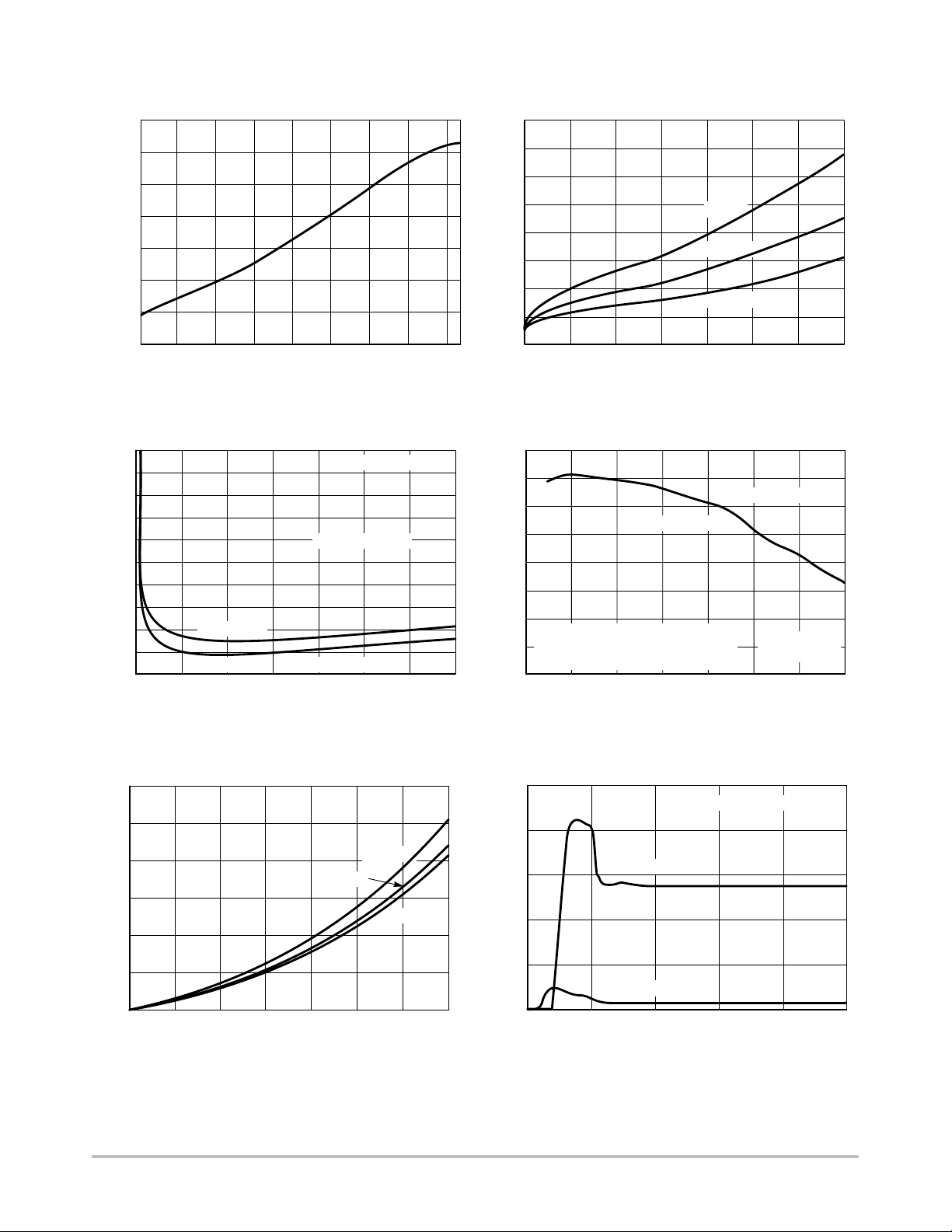
TYPICAL PERFORMANCE CHARACTERISTICS
0.4
0.3
0.2
0.1
0.0
−0.1
TRACKING ERROR (mV)
−0.2
−0.3
−20 1200 20 40 60 80 100
−40
Figure 2. Tracking Error vs. Temperature
50
45
40
35
30
25
ESR ()
20
15
10
5
0
0
C2 = 10 F
C2 = 0.1 F
10 20 30 40 70
OUTPUT CURRENT (mA)
TEMPERATURE (°C)
Unstable Region
Stable Region
V
OUT
= 5.0 V
6050
1.0
0.8
0.6
0.4
0.2
0.0
−0.2
TRACKING ERROR (mV)
−0.4
−0.6
0
20 30 5040 60 70
10
OUTPUT CURRENT (mA)
Figure 3. Tracking Error vs. Output Current
4.0
3.5
3.0
2.5
2.0
ESR ()
1.5
1.0
Data is for 0.1 F only. Capacitor
values 0.5 F and above do not
0.5
exhibit instability with low ESR.
0.0
0
10 20 30 40 70
OUTPUT CURRENT (mA)
−40°C
+25°C
+125°C
Unstable Region
Stable Region
C2 = 0.1 F
V
OUT
= 5.0 V
6050
Figure 4. Output Stability with Capacitor Change Figure 5. Output Stability with 0.1 F at Low ESR
12
10
8
6
4
2
QUIESCENT CURRENT (mA)
0
10 20 30 40 50 60 70
0
OUTPUT CURRENT (mA)
+125°C
+25°C
−40°C
2.5
2
I
= 20 mA
1.5
1
0.5
QUIESCENT CURRENT (mA)
0
0
OUT
I
= 1 mA
OUT
510 2515 20
INPUT VOLTAGE (V)
V
/ ENABLE = 5.0 V
REF
Figure 6. Quiescent Current vs. Output Current Figure 7. Quiescent Current vs. Input Voltage
http://onsemi.com
4
Page 5
NCV8184
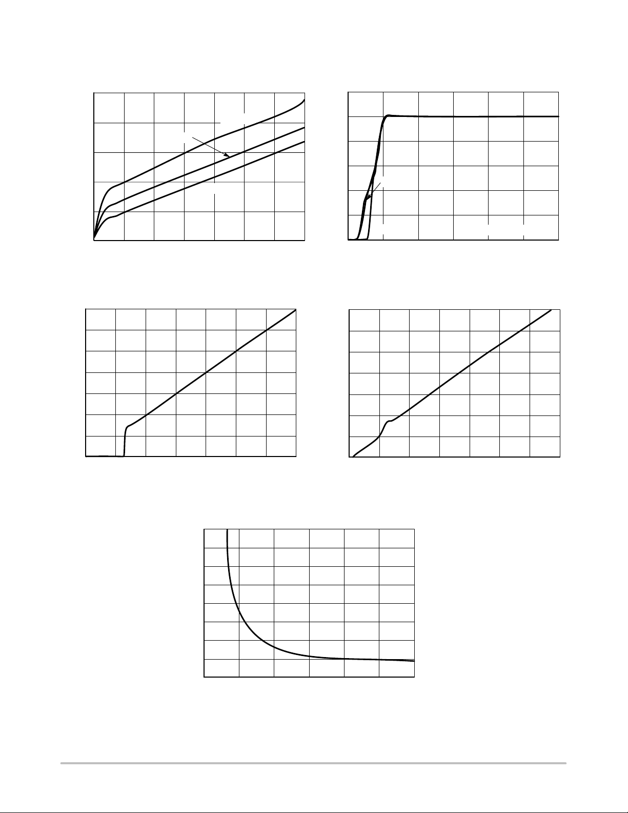
TYPICAL PERFORMANCE CHARACTERISTICS
0.5
0.4
0.3
0.2
DROPOUT VOLTAGE (V)
0.1
0.0
+25°C
0
10
20 30 5040 60 70
OUTPUT CURRENT (mA)
+125°C
−40°C
Figure 8. Dropout Voltage vs. Output Current
7
6
5
4
6
5
(V)
OUT
4
+25°C
3
2
1
OUTPUT VOLTAGE V
0
0
+125°C
−40°C
5101520
INPUT VOLTAGE V
V
/ENABLE = 5.0 V
REF
(V)
IN
Figure 9. Output Voltage vs. Input Voltage
0.7
0.6
0.5
0.4
25
30
3
2
OUTPUT VOLTAGE (V)
1
0
01
234567
REFERENCE VOLTAGE (V)
Figure 10. Output Voltage vs. Reference Voltage
120
115
110
, (°C/W)
105
JA
100
95
90
TO AMBIENT, R
85
THERMAL RESISTANCE, JUNCTION
80
0
1234 65
0.3
0.2
REFERENCE CURRENT (A)
0.1
0.0
COPPER AREA (in2)
01234567
REFERENCE VOLTAGE (V)
Figure 11. Reference Current vs. Reference
Voltage
Figure 12. SO−8, JA as a Function of the Pad
Copper Area (2.0 oz. Cu Thickness),
Board Material = 0.0625 G−10/R−4
http://onsemi.com
5
Page 6

NCV8184
F
CIRCUIT DESCRIPTION
ENABLE Function
By pulling the V
/ENABLE lead below 0.8 V, (see
REF
Figure 16 or Figure 17), the IC is disabled and enters a sleep
state where the device draws less than 20 A from supply.
When the V
tracks the V
Loads
C2**
10 F
Figure 13. Tracking Regulator at the Same Voltage
Loads
C2**
10 F
/ENABLE lead is greater than 2.1 V, V
REF
/ENABLE lead normally.
REF
, 70 mA
V
V
OUT
OUT
, 70 mA
V
OUT
GND
GND
Adj
V
OUT
V
OUT
GND
GND
Adj
V
GND
GND
NCV8184
V
REF
ENABLE
V
REF
V
GND
GND
NCV8184
V
REF
ENABLE
IN
/
IN
/
C3***
10 nF
C3***
10 nF
C1*
1.0 F
C1*
1.0 F
R1
R2
OUT
B+
5.0 V
B+
V
REF
Output Voltage
The output is capable of supplying 70 mA to the load
while configured as a similar (Figure 13), lower (Figure 15),
or higher (Figure 14) voltage as the reference lead. The Adj
lead acts as the inverting terminal of the op amp and the
V
lead as the non−inverting.
REF
The device can also be configured as a high−side driver as
displayed in Figure 18.
, 70 mA
V
C2**
10 F
OUT
R
R
V
OUT
GND
F
A
GND
Adj
V
OUT
V
GND
GND
NCV8184
V
REF
ENABLE
V
REF
IN
/
R
(1
R
C3***
10 nF
E
)
A
C1*
1.0 F
Figure 14. Tracking Regulator at Higher Voltages
, 70 mA
V
C2**
10 F
OUT
V
OUT
GND
GND
Adj
V
GND
GND
NCV8184
V
REF
ENABLE
IN
/
C3***
10 nF
C1*
1.0 F
R
B+
V
B+
V
RE
REF
Loads
from MCU
V
OUT
V
REF
R2
(
R1 R2
)
Figure 15. Tracking Regulator at Lower Voltages
6.0 V−40 V
70 mA
To Load
(e.g. sensor)
100 nF
10 F
V
IN
NCV8501
V
OUT
GND
GND
Adj
V
GND
GND
NCV8184
V
REF
ENABLE
IN
/
V
(5.0 V)
REF
C1*
1.0 F
I/O
C3***
10 nF
Figure 17. Alternative ENABLE Circuit
* C1 is required if the regulator is far from the power source filter.
** C2 is required for stability.
*** C3 is recommended for EMC susceptibility
Figure 16. Tracking Regulator with ENABLE Circuit
V
IN
GND
GND
NCV8184
/
V
REF
ENABLE
B V
C3***
10 nF
SAT
C
V
V
GND
GND
Adj
OUT
OUT
Figure 18. High−Side Driver
B+70 mA
MCU
http://onsemi.com
6
Page 7

NCV8184
APPLICATION NOTES
V
Short to Battery
OUT
The NCV8184 will survive a short to battery when hooked
up the conventional way as shown in Figure 19. No damage
to the part will occur. The part also endures a short to battery
when powered by an isolated supply at a lower voltage as in
Short to battery
Figure 20. In this case the NCV8184 supply input voltage is
set at 7 V when a short to battery (14 V typical) occurs on
V
which normally runs at 5 V. The current into the
OUT
device (ammeter in Figure 20) will draw additional current
as displayed in Figure 21.
V
70 mA
C2**
10 F
OUT
V
OUT
GND
GND
Adj
V
OUT
GND
GND
NCV8184
V
ENABLE
= V
REF
Loads
Figure 19.
Short to battery
A
Automotive Battery
typically 14 V
* C1 is required if the regulator is far from the power source filter.
** C2 is required for stability.
*** C3 is recommended for EMC susceptibility.
Loads
C2**
10 F
V
OUT
70 mA
Figure 20.
V
REF
B+
IN
/
V
GND
GND
Adj
OUT
V
C3***
10 nF
OUT
C1*
1.0 F
V
GND
GND
NCV8184
V
REF
ENABLE
= V
REF
+
Automotive Battery
typically 14 V
−
5.0 V
+
5.0 V
−
B+
IN
/
C1*
1.0 F
C3***
10 nF
7 V
5.0 V
+
5.0 V
−
+
−
18
16
14
12
10
8
6
CURRENT (mA)
4
2
0
6510152025
7 8 9 11121314 16171819 2122 2324 26
V
VOLTAGE (V)
OUT
Figure 21. V
Short to Battery
OUT
http://onsemi.com
Switched Application
The NCV8184 has been designed for use in systems where
the reference voltage on the V
/ENABLE pin is
REF
continuously on. Typically, the current into the
V
/ENABLE pin will be less than 1.0 A when the
REF
voltage on the VIN pin (usually the ignition line) has been
switched out (VIN can be at high impedance or at ground.)
Reference Figure 22.
Ignition
V
OUT
C2
10 F
V
OUT
GND
GND
Adj
V
GND
GND
NCV8184
V
REF
ENABLE
IN
/
< 1.0 A
Figure 22.
7
Switch
C1
1.0 F
V
REF
5.0 V
V
BAT
Page 8

NCV8184
External Capacitors
The output capacitor for the NCV8184 is required for
stability. Without it, the regulator output will oscillate.
Actual size and type may vary depending upon the
application load and temperature range. Capacitor effective
series resistance (ESR) is also a factor in the IC stability.
Worst−case is determined at the minimum ambient
temperature and maximum load expected.
The output capacitor can be increased in size to any
desired value above the minimum. One possible purpose of
this would be to maintain the output voltage during brief
conditions of negative input transients that might be
characteristic of a particular system.
The capacitor must also be rated at all ambient
temperatures expected in the system. To maintain regulator
stability down to −40°C, a capacitor rated at that temperature
must be used.
More information on capacitor selection for SMART
REGULATORs is available in the SMART REGULATOR
application note, “Compensation for Linear Regulators,”
document number SR003AN/D, available through our
website at http://www.onsemi.com.
Calculating Power Dissipation in a Single Output
Linear Regulator
The maximum power dissipation for a single output
regulator (Figure 23) is:
PD(max) {VIN(max) V
VIN(max)I
Q
OUT
(min)}I
OUT
(max)
(eq. 1)
where:
V
V
I
OUT(max)
is the maximum input voltage,
IN(max)
OUT(min)
is the minimum output voltage,
is the maximum output current, for the
application,and
IQ is the quiescent current the regulator consumes at
I
OUT(max)
.
Once the value of PD(max) is known, the maximum
permissible value of R
R
can be calculated:
JA
150°C T
JA
A
P
D
(eq. 2)
The value of R
can then be compared with those in the
JA
Package Thermal Data Section of the data sheet. Those
packages with R
’s less than the calculated value in
JA
equation 2 will keep the die temperature below 150°C.
In some cases, none of the packages will be sufficient to
dissipate the heat generated by the IC, and an external heat
sink will be required.
I
V
IN
Heatsinks
IN
Figure 23. Single Output Regulator with Key
Performance Parameters Labeled
SMART
REGULATOR
Control
Features
I
Q
I
OUT
V
OUT
A heatsink effectively increases the surface area of the
package to improve the flow of heat away from the IC and
into the surrounding air.
Each material in the heat flow path between the IC and the
outside environment will have a thermal resistance. Like
series electrical resistances, these resistances are summed to
determine the value of R
R
R
JA
JC
JA:
R
CS
R
SA
(eq. 3)
where:
R
= the junction−to−case thermal resistance,
JC
R
= the case−to−heatsink thermal resistance, and
CS
R
= the heatsink−to−ambient thermal resistance.
SA
R
appears in the package section of the data sheet. Like
JC
R
, it is a function of package type. R
JA
CS
and R
are
SA
functions of the package type, heatsink and the interface
between them. These values appear in heat sink data sheets
of heatsink manufacturers.
http://onsemi.com
8
Page 9

NCV8184
PACKAGE THERMAL DATA
Test Conditions
Parameter
SO−8 Package Min−Pad Board (Figure 24) 1.0 in Pad Board (Figure 25)
Junction−to−Case top (−JT, JT) 39 32 °C/W
Junction−to−Pin 8 (−JL8,
Junction−to−Ambient (R
DPAK 5−Pin Package 0.5 in2 Spreader Board (Figure 26) 1.0 in2 Spreader Board (Figure 27)
Junction−to−Board (−JB, JB) 15 15 °C/W
Junction−to−Pin 3 (tab) (−JL3,
Junction−to−Ambient (R
) 63 58 °C/W
JL8
, JA) 121 98 °C/W
JA
) 16 16 °C/W
JL3
, JA) 100 69 °C/W
JA
Typical Value
Units
Figure 24. 2.0 oz. copper, 40 mil traces
Figure 26. 1.0 oz. copper, 0.3 in
2
drain pad,
0.5 in2 including traces
Figure 25. 1.0 oz. copper,
approx. 1/8 in
2
per lead, 1.0 in2 total
Figure 27. 2.0 oz. copper, 0.5 in
2
pad, 1.0 in
including traces
2
drain
http://onsemi.com
9
Page 10

NCV8184
T able 1. SO−8 Thermal RC Network Models*
Board Type Min−Pad 1.0 inch Pad Min−Pad 1.0 inch Pad
(SPICE Deck Format) Cauer Network Foster Network
Min 1.0 inch Units Tau Tau Units
C_C1 Junction Gnd 7.06879E−7 7.06879E−7 W−s/C 2.99E−7 2.99E−7 sec
C_C2 node1 Gnd 3.34499E−6 3.34499E−6 W−s/C 4.40E−6 4.40E−6 sec
C_C3 node2 Gnd 1.00350E−5 1.00350E−5 W−s/C 4.48E−5 4.48E−5 sec
C_C4 node3 Gnd 3.68358E−5 3.68358E−5 W−s/C 2.46E−4 2.46E−4 sec
C_C5 node4 Gnd 4.29554E−4 4.29554E−4 W−s/C 4.72E−3 4.72E−3 sec
C_C6 node5 Gnd 7.20791E−3 7.20791E−3 W−s/C 7.18E−2 7.25E−2 sec
C_C7 node6 Gnd 3.52182E−2 3.76156E−2 W−s/C 1.61E+0 1.31E+0 sec
C_C8 node7 Gnd 7.16622E−1 1.33747E+0 W−s/C 2.08E+1 1.62E+1 sec
C_C9 node8 Gnd 6.57830E+0 3.97588E+0 W−s/C 1.33E+2 1.08E+2 sec
Min 1.0 inch R’s R’s
R_R1 Junction node1 5.17805E−1 5.1780E−1 °C/W 0.34137 0.34137 °C/W
R_R2 node1 node2 1.55341E+0 1.5534E+0 °C/W 0.83581 0.83581 °C/W
R_R3 node2 node3 4.66024E+0 4.6602E+0 °C/W 2.36526 2.36526 °C/W
R_R4 node3 node4 4.98386E+0 4.9838E+0 °C/W 6.76959 6.76960 °C/W
R_R5 node4 node5 1.04570E+1 1.0457E+1 °C/W 10.39190 10.39200 °C/W
R_R6 node5 node6 1.14509E+1 1.1450E+1 °C/W 8.68648 8.81855 °C/W
R_R7 node6 node7 3.94880E+1 2.9500E+1 °C/W 38.62760 31.37390 °C/W
R_R8 node7 node8 3.10554E+1 1.6877E+1 °C/W 27.65780 8.93175 °C/W
R_R9 node8 node9 1.77562E+1 1.8812E+1 °C/W 26.24690 28.98470 °C/W
Table 2. DPAK 5−Lead Thermal RC Network Models*
Drain Copper Area (1 oz thick) 100 mm
2
(SPICE Deck Format) Cauer Network Foster Network
100 mm
2
C_C1 Junction Gnd 1.51E−06 1.51E−06 W−s/C 1.00E−06 1.00E−06 sec
C_C2 node1 Gnd 6.00E−06 5.91E−06 W−s/C 1.00E−05 1.00E−05 sec
C_C3 node2 Gnd 1.90E−05 1.81E−05 W−s/C 1.00E−04 1.00E−04 sec
C_C4 node3 Gnd 1.05E−04 9.59E−05 W−s/C 7.00E−04 6.00E−04 sec
C_C5 node4 Gnd 2.98E−03 3.21E−03 W−s/C 1.03E−02 1.03E−02 sec
C_C6 node5 Gnd 2.37E−02 7.87E−02 W−s/C 1.71E−01 1.71E−01 sec
C_C7 node6 Gnd 4.95E−02 7.88E−02 W−s/C 1.17E+00 1.17E+00 sec
C_C8 node7 Gnd 2.32E−01 1.03E+00 W−s/C 7.63E+00 7.63E+00 sec
C_C9 node8 Gnd 6.95E−01 1.58E+00 W−s/C 3.93E+01 3.93E+01 sec
C_C10 node9 Gnd 6.91E+00 1.16E+01 W−s/C 1.42E+02 1.42E+02 sec
100 mm
2
R_R1 Junction node1 0.845 0.850 °C/W 0.507 0.507 °C/W
R_R2 node1 node2 1.886 1.933 °C/W 1.096 1.096 °C/W
R_R3 node2 node3 4.758 5.070 °C/W 3.467 3.467 °C/W
R_R4 node3 node4 5.336 4.862 °C/W 7.168 7.168 °C/W
R_R5 node4 node5 3.735 3.201 °C/W 3.394 3.394 °C/W
R_R6 node5 node6 10.537 5.293 °C/W 4.000 0.720 °C/W
R_R7 node6 node7 19.583 6.828 °C/W 15.000 8.912 °C/W
R_R8 node7 node8 38.068 13.172 °C/W 20.000 3.636 °C/W
R_R9 node8 node9 43.000 16.466 °C/W 50.000 15.161 °C/W
R_R10 node9 gnd 16.884 8.868 °C/W 40.000 22.480 °C/W
*Bold face items in the tables above represent the package without the external thermal system.
653 mm
653 mm
653 mm
2
2
Units Tau Tau Units
2
100 mm
2
653 mm
R’s R’s
2
http://onsemi.com
10
Page 11

NCV8184
The Cauer networks generally have physical significance
and may be divided between nodes to separate thermal
behavior due to one portion of the network from another.
The Foster networks, though when sorted by time constant
(as above) bear a rough correlation with the Cauer networks,
are really only convenient mathematical models. Cauer
tools, whereas Foster networks may be more easily
implemented using mathematical tools (for instance, in a
spreadsheet program), according to the following formula:
R(t)
n
i 1
−ttau
R
1−e
i
networks can be easily implemented using circuit simulating
Copper Area (in2)
0 0.1 0.2 0.3 0.4 0.5 0.6 0.7 0.8 0.9 1 1.1
160
150
140
130
120
110
(°C/W)
100
JA
90
80
70
60
50
0 100 200 300 400 500 600 700
2.0 oz. Cu
Copper Area (mm
1.0 oz. Cu
2
)
i
Figure 28. DP AK 5−Lead, JA as a Function of the Pad Copper Area Including Traces,
100
50% Duty Cycle
20%
10%
10
1.0 in. pad (°C/W)
JA
R
5%
2%
1%
1
0.000001 0.00001
Board Material 0.62” Thick FR4
Non−Normalized Response
0.0001 0.001
0.01
Pulse Width (s)
0.1
1
10 100 1000
Figure 29. SO−8 Thermal Duty Cycle Curves on 1.0 in. Spreader Test Board
http://onsemi.com
11
Page 12

NCV8184
100
50% Duty Cycle
20%
10
10%
5%
(°C/W)
R
2%
1
1%
Single Pulse
(1.0 in pad PCB) Die Size = 2.08 x 1.55 x 0.40 5.0% Active Area
EFFECTIVE THERMAL RESISTANCE
0.1
0.000001 0.00001 0.0001 0.001 0.01 0.1 1 10 100 1000
t1 (s)
Figure 30. DPAK 5−Lead Thermal Duty Cycle Curves on 1.0 in. Spreader Test Board
1000
Die Size = 2.08 x 1.55 x 0.40 5.0% Active Area
100
Notes:
P
DM
t
1
t
2
Duty Cycle, D =
min pad (Cu Area = 100 mm2)
t
1
t
2
1.0 in pad (Cu Area = 653 mm2)
(°C/W)
R
10
1
0.1
0.000001 0.00001 0.0001 0.001 0.01 0.1 1 10 100 1000
Time (s)
Figure 31. DPAK 5−Lead Thermal Transient Response on Typical Test Boards
Junction
R
1
C
1
Time constants are
Amplitudes of mathematical solution are
R
2
C
2
not
simple RC products.
R
3
C
3
not
the resistance values.
R
n
C
n
Ambient
(thermal ground)
Figure 32. Grounded Capacitor Thermal Network (“Cauer” Ladder)
Junction
R
1
R
2
R
3
R
n
C
1
C
2
C
3
Each rung is exactly characterized by its RC−product time constant;
Amplitudes are the resistances
Figure 33. Non−Grounded Capacitor Thermal Ladder (“Foster” Ladder)
http://onsemi.com
12
C
n
Ambient
(thermal ground)
Page 13
NCV8184
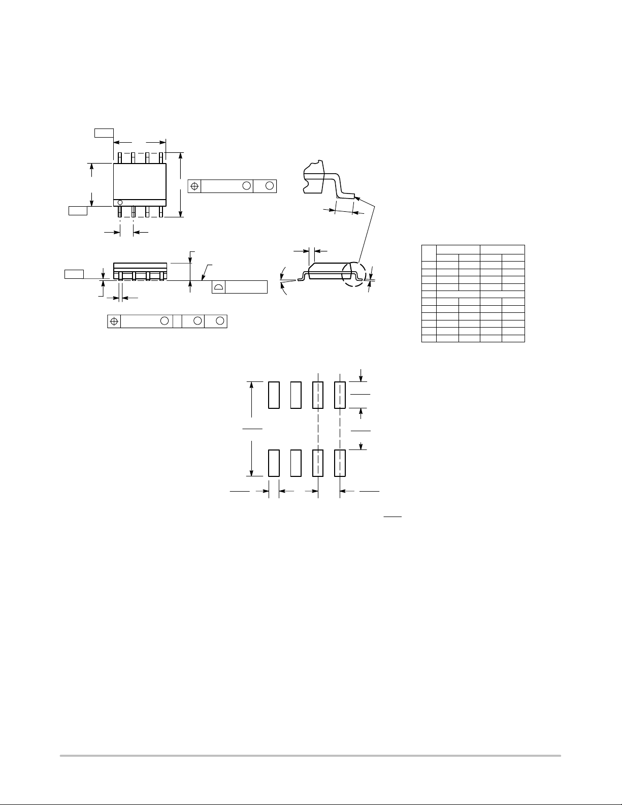
PACKAGE DIMENSIONS
SO−8
D SUFFIX
CASE 751−07
ISSUE AB
−Y−
−Z−
−X−
A
58
B
1
S
0.25 (0.010)
4
M
M
Y
K
G
C
SEATING
PLANE
0.10 (0.004)
H
D
0.25 (0.010) Z
M
Y
SXS
N
X 45
M
J
NOTES:
1. DIMENSIONING AND TOLERANCING PER ANSI
Y14.5M, 1982.
2. CONTROLLING DIMENSION: MILLIMETER.
3. DIMENSION A AND B DO NOT INCLUDE MOLD
PROTRUSION.
4. MAXIMUM MOLD PROTRUSION 0.15 (0.006) PER
SIDE.
5. DIMENSION D DOES NOT INCLUDE DAMBAR
PROTRUSION. ALLOWABLE DAMBAR
PROTRUSION SHALL BE 0.127 (0.005) TOTAL IN
EXCESS OF THE D DIMENSION AT MAXIMUM
MATERIAL CONDITION.
6. 751−01 THRU 751−06 ARE OBSOLETE. NEW
STANDAARD IS 751−07
MILLIMETERS
DIMAMIN MAX MIN MAX
4.80 5.00 0.189 0.197
B 3.80 4.00 0.150 0.157
C 1.35 1.75 0.053 0.069
D 0.33 0.51 0.013 0.020
G 1.27 BSC 0.050 BSC
H 0.10 0.25 0.004 0.010
J 0.19 0.25 0.007 0.010
K 0.40 1.27 0.016 0.050
M 0 8 0 8
N 0.25 0.50 0.010 0.020
S 5.80 6.20 0.228 0.244
INCHES
SOLDERING FOOTPRINT
1.52
0.060
7.0
0.275
4.0
0.155
0.6
0.024
SCALE 6:1
http://onsemi.com
13
1.270
0.050
inches
mm
Page 14

NCV8184
PACKAGE DIMENSIONS
DPAK 5−LEAD CENTER LEAD CROP
DT SUFFIX
CASE 175AA−01
ISSUE O
NOTES:
SEATING
−T−
PLANE
B
V
S
R
A
1234 5
K
F
L
D
5 PL
G
0.13 (0.005) T
C
E
R1
Z
U
J
H
M
1. DIMENSIONING AND TOLERANCING
PER ANSI Y14.5M, 1982.
2. CONTROLLING DIMENSION: INCH.
DIM MIN MAX MIN MAX
A 0.235 0.245 5.97 6.22
B 0.250 0.265 6.35 6.73
C 0.086 0.094 2.19 2.38
D 0.020 0.028 0.51 0.71
E 0.018 0.023 0.46 0.58
F 0.024 0.032 0.61 0.81
G 0.180 BSC 4.56 BSC
H 0.034 0.040 0.87 1.01
J 0.018 0.023 0.46 0.58
K 0.102 0.114 2.60 2.89
L 0.045 BSC 1.14 BSC
R 0.170 0.190 4.32 4.83
R1 0.185 0.210 4.70 5.33
S 0.025 0.040 0.63 1.01
U 0.020 −−− 0.51 −−−
V 0.035 0.050 0.89 1.27
Z 0.155 0.170 3.93 4.32
MILLIMETERSINCHES
Note: Pin 3 and the tab are internally connected
SMART REGULATOR is a registered trademark of Semiconductor Components Industries, LLC (SCILLC).
ON Semiconductor and are registered trademarks of Semiconductor Components Industries, LLC (SCILLC). SCILLC reserves the right to make changes without further notice
to any products herein. SCILLC makes no warranty, representation or guarantee regarding the suitability of its products for any particular purpose, nor does SCILLC assume any liability
arising out of the application or use of any product or circuit, and specifically disclaims any and all liability, including without limitation special, consequential or incidental damages.
“Typical” parameters which may be provided in SCILLC data sheets and/or specifications can and do vary in different applications and actual performance may vary over time. All
operating parameters, including “Typicals” must be validated for each customer application by customer’s technical experts. SCILLC does not convey any license under its patent rights
nor the rights of others. SCILLC products are not designed, intended, or authorized for use as components in systems intended for surgical implant into the body, or other applications
intended to support or sustain life, or for any other application in which the failure of the SCILLC product could create a situation where personal injury or death may occur. Should
Buyer purchase or use SCILLC products for any such unintended or unauthorized application, Buyer shall indemnify and hold SCILLC and its officers, employees, subsidiaries, affiliates,
and distributors harmless against all claims, costs, damages, and expenses, and reasonable attorney fees arising out of, directly or indirectly, any claim of personal injury or death
associated with such unintended or unauthorized use, even if such claim alleges that SCILLC was negligent regarding the design or manufacture of the part. SCILLC is an Equal
Opportunity/Affirmative Action Employer. This literature is subject to all applicable copyright laws and is not for resale in any manner.
PUBLICATION ORDERING INFORMATION
LITERATURE FULFILLMENT:
Literature Distribution Center for ON Semiconductor
P.O. Box 5163, Denver, Colorado 80217 USA
Phone: 303−675−2175 or 800−344−3860 Toll Free USA/Canada
Fax: 303−675−2176 or 800−344−3867 Toll Free USA/Canada
Email: orderlit@onsemi.com
N. American Technical Support: 800−282−9855 Toll Free
USA/Canada
Japan: ON Semiconductor, Japan Customer Focus Center
2−9−1 Kamimeguro, Meguro−ku, Tokyo, Japan 153−0051
Phone: 81−3−5773−3850
http://onsemi.com
14
ON Semiconductor Website: http://onsemi.com
Order Literature: http://www.onsemi.com/litorder
For additional information, please contact your
local Sales Representative.
NCV8184/D
 Loading...