

Page 1
查询NCV8141供应商
NCV8141
5.0 V, 500 mA Linear
Regulator with ENABLE,
RESET
, and Watchdog
The NCV8141 is a linear regulator suited for microprocessor
applications in automotive environments.
This ON Semiconductor part provides the power for the
microprocessors along with many of the control functions needed in
today’s computer based systems. Incorporating all of these features
saves both cost, and board space.
The NCV8141 provides a low sleep mode current as compared to
the CS8141. Consult your local sales representative for a low sleep
mode current version of the CS8140.
Features
• 5.0 V ±4.0%, 500 mA Output Voltage
• Lower Quiescent Current
• Improved Filtering for /RESET Functionality
• P Compatible Control Functions
♦ Watchdog
♦ RESET
♦ ENABLE
• Low Dropout Voltage (1.25 V @ 500 mA)
• Low Quiescent Current (7.0 mA @ 500 mA)
• Low Noise, Low Drift
• Low Current SLEEP Mode 50 A (max)
• Fault Protection
♦ Thermal Shutdown
♦ Short Circuit
♦ 60 V Peak Transient Voltage
• NCV Prefix for Automotive and Other Applications Requiring Site
and Control Changes
• Pb−Free Package is Available*
http://onsemi.com
D2PAK−7
DPS SUFFIX
1
7
1
ORDERING INFORMATION
Device Package Shipping
CASE 936AB
A = Assembly Location
WL = Wafer Lot
Y = Year
WW = Work Week
PIN CONNECTIONS
Tab = GND
Pin 1. V
2. ENABLE
3. RESET
4. GND
5. Delay
6. WDI
7. V
MARKING
DIAGRAM
NCV8141
AWLYWW
1
IN
OUT
†
*For additional information on our Pb−Free strategy and soldering details, please
download the ON Semiconductor Soldering and Mounting Techniques
Reference Manual, SOLDERRM/D.
Semiconductor Components Industries, LLC, 2004
August, 2004 − Rev. 5
1 Publication Order Number:
NCV8141D2T D2PAK 50 Units/Rail
NCV8141D2TG D2PAK
(Pb−Free)
NCV8141D2TR4 D2PAK 750 Tape & Reel
†For information on tape and reel specifications,
including part orientation and tape sizes, please
refer to our Tape and Reel Packaging Specifications
Brochure, BRD8011/D.
50 Units/Rail
NCV8141/D
Page 2
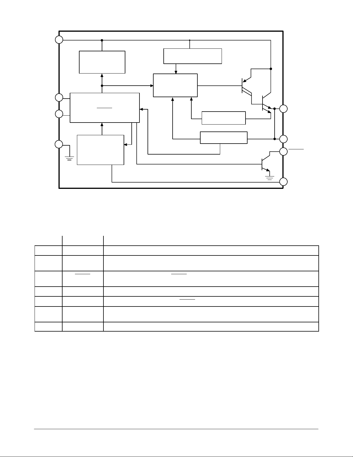
NCV8141
V
IN
Overvoltage
Reference & Bias
Overtemperature
Regulation
ENABLE
WDI
Control Logic
ENABLE
RESET
Delay
GND
Watchdog
Figure 1. Block Diagram
PIN FUNCTION DESCRIPTION
Pin Symbol Function
1 V
IN
2 ENABLE CMOS compatible logical input. V
Supply voltage to IC, usually direct from the battery.
is disabled when ENABLE is LOW and WDI is beyond its
preset limits.
OUT
Short Circuit
Undervoltage
V
OUT
Sense
RESET
Delay
3 RESET CMOS compatible output lead. RESET goes low whenever V
value for more than 2.0 s or WDI signal falls outside it’s window limits.
drops below 4.5% of it’s typical
OUT
4 GND Ground Connection.
5 Delay Timing capacitor for Watchdog and RESET functions.
6 WDI CMOS compatible input lead. The Watchdog function monitors the falling edge of the incoming digital
pulse train. The signal is usually generated by the system microprocessor.
7 V
OUT
Regulated output voltage, 5.0 V (typ).
http://onsemi.com
2
Page 3
NCV8141
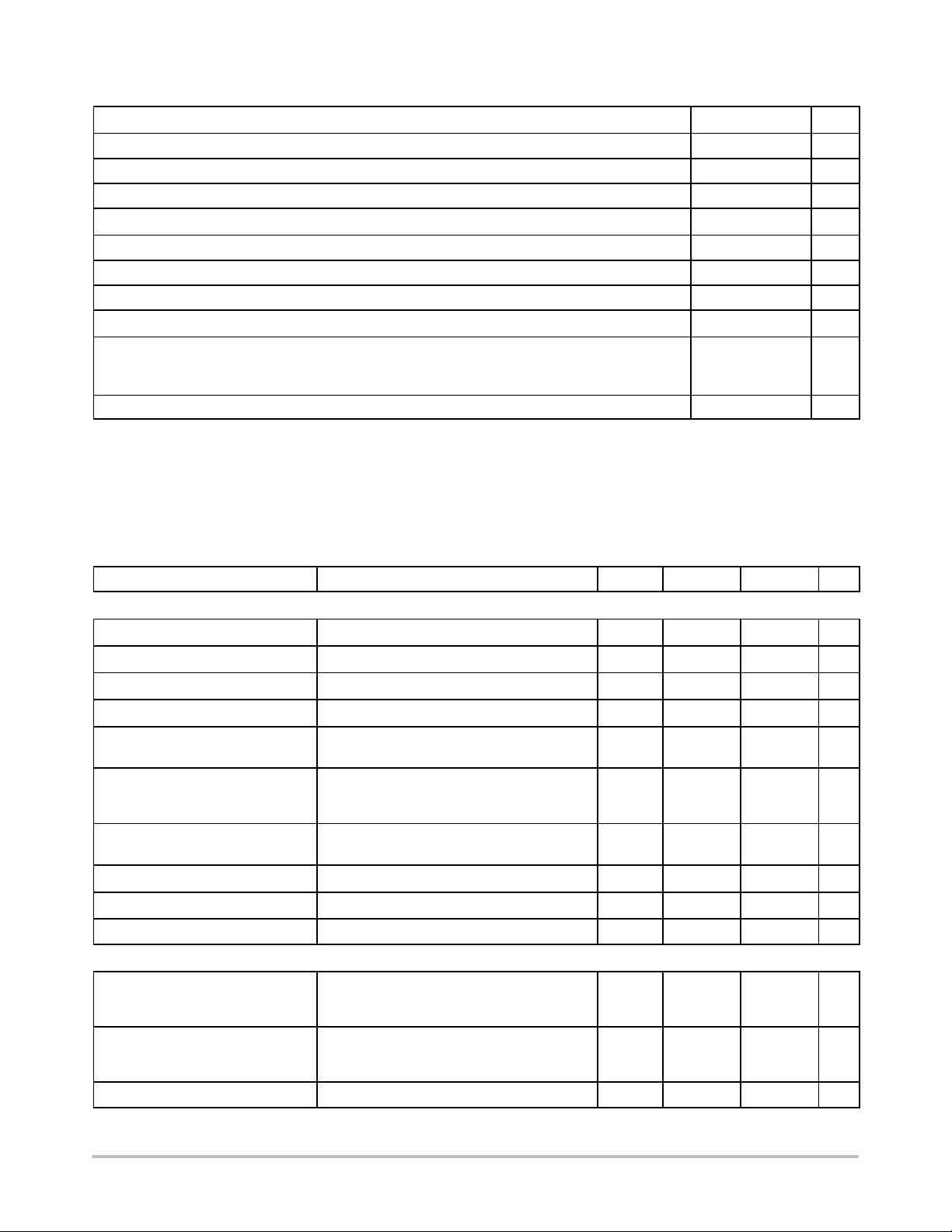
MAXIMUM RATINGS
Rating Value Unit
Input Operating Range −0.5 to 26 V
Peak Transient Voltage (46 V Load Dump @ 14 V V
Electrostatic Discharge (Human Body Model) 4.0 kV
WDI Input Signal Range −0.3 to 7.0 V
Internal Power Dissipation Internally Limited −
Junction Temperature Range (TJ) −40 to +150 °C
Storage Temperature Range −65 to +150 °C
) 60 V
BAT
ENABLE −0.3 to V
IN
V
Package Thermal Resistance, D2PAK 7−Pin
Junction−to−Case, R
Junction−to−Ambient, R
JC
JA
1.5
10−50†
°C/W
°C/W
Lead Temperature Soldering: Reflow (SMD styles only) (Note 1) 225 peak (Note 2) °C
Maximum ratings are those values beyond which device damage can occur. Maximum ratings applied to the device are individual stress limit
values (not normal operating conditions) and are not valid simultaneously . If these limits are exceeded, device functional operation is not implied,
damage may occur and reliability may be affected.
= R
+ R
†Depending on thermal properties of substrate R
1. 60 seconds max above 183°C.
JA
JC
.
CA
2. −5.0°C/+0°C allowable conditions.
ELECTRICAL CHARACTERISTICS (7.0 ≤ V
≤26 V , 5 .0 m A ≤ I
IN
≤500 mA, −40°C ≤ TJ ≤150°C, −40°C ≤ TA ≤125°C, u nle ss o the rwise
OUT
noted.) (Note 3)
Characteristic
Output Stage (V
Output Voltage, V
Dropout Voltage (VIN − V
OUT
OUT
)
) I
OUT
7.0 V ≤ VIN ≤ 26 V, 5.0 mA < I
Line Regulation I
Load Regulation VIN = 14 V, 50 mA ≤ I
Output Impedance, R
OUT
Test Conditions Min Typ Max Unit
< 500 mA 4.8 5.0 5.2 V
OUT
= 500 mA − 1.25 1.50 V
OUT
= 50 mA, 7.0 V ≤ VIN ≤ 26 V, − 5.0 25 mV
OUT
≤ 500 mA − 5.0 80 mV
OUT
500 mA DC and 10 mA AC,
− 200 − m
100 Hz ≤ f ≤ 10 kHz
Quiescent Current, (IQ)
Active Mode
Sleep Mode
Ripple Rejection 7 .0 V ≤ VIN ≤ 17 V, I
Current Limit VIN = 7.0 V, V
0 ≤ I
≤ 500 mA, 7.0 V ≤ VIN ≤ 26 V
OUT
= 0 mA, VIN = 13 V, ENABLE = 0 V
I
OUT
= 250 mA,
OUT
f = 120 Hz
= 4.5 V 600 1200 2000 mA
OUT
−
−
7.0
25
15
50
60 75 − dB
Thermal Shutdown Guaranteed by Design 150 180 − °C
Overvoltage Shutdown V
< 1.0 V 30 34 38 V
OUT
ENABLE
Threshold
HIGH
LOW
V
V
OUT
OUT
≥ 0.5 V, (V
< 0.5 V, (V
OUT(ON)
OUT(OFF)
)
)
3.5
−
4.05
3.95
4.50
−
Input Current
HIGH
LOW
ENABLE = 5.0 V
ENABLE = 0 V
−
−1.0
35
0
1.0
75
Threshold Hysteresis (HIGH − LOW) − 80 − mV
3. To observe safe operating junction temperatures, low duty cycle pulse testing is used in tests where applicable.
http://onsemi.com
3
mA
A
V
V
A
A
Page 4
NCV8141
ELECTRICAL CHARACTERISTICS (continued) (7.0 ≤ V
≤ 26 V, 5.0 mA ≤ I
IN
≤ 500 mA, −40°C ≤ TJ ≤ 150°C, −40°C ≤ TA ≤
OUT
125°C, unless otherwise noted.) (Note 4)
Characteristic
Test Conditions Min Typ Max Unit
RESET
Threshold HIGH V
Threshold LOW V
R(HI)
R(LOW)
V
Increasing 4.65 4.90 V
OUT
V
Decreasing 4.50 4.70 4.90 V
OUT
OUT
− 0.05 V
Threshold Hysteresis (VRH) (HIGH − LOW) 150 200 250 mV
RESET Output Leakage
RESET = HIGH
Output Voltage Low (V
Output Voltage Low (V
Delay Times t
Delay Times t
POR
WDI(RESET)
) 1.0 V ≤ V
L(LOW)
) V
Rpeak
V
≥ V
OUT
R(HI)
≤ V
OUT
, Power up, Power down − 0.6 1.0 V
OUT
C
C
, RP = 2.7 k (Note 5) − 0.1 0.4 V
R(LOW)
= 0.1 F 30 47.5 65 ms
DELAY
= 0.1 F 0.5 1.0 1.5 ms
DELAY
− − 25 A
Watchdog
Input Voltage High
− 2.0 − − V
Input Voltage Low − − − 0.8 V
Input Current WDI ≤ V
Threshold Frequency f
WDI
C
= 0.1 F 64 77 96 Hz
DELAY
OUT
− 0 10 A
4. To observe safe operating junction temperatures, low duty cycle pulse testing is used in tests where applicable.
is connected to RESET and V
5. R
P
OUT.
1000
100
10
ESR ()
0.1
0.01
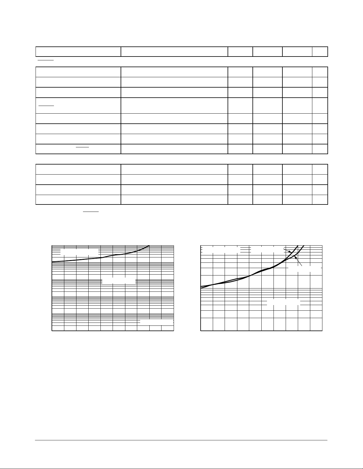
TYPICAL PERFORMANCE CHARACTERISTICS
1000
ESR ()
100
10
0
Unstable Region
550
10 20 30 4015
Output Current (mA)
Unstable Region
Stable Region
1
C
= 10 F
vout
0
10 20 30 4015
550
25 35 45
Output Current (mA)
Figure 2. Output Stability Figure 3. Output Stability with Capacitor Change
C
= 10 F
vout
C
vout
Stable Region
25 35 45
= 0.1 F
http://onsemi.com
4
Page 5

NCV8141
DEFINITION OF TERMS
Dropout Voltage: The input−output voltage differential
at which the circuit ceases to regulate against further
reduction in input voltage. Measured when the output
voltage has dropped 100 mV from the nominal value
obtained at 14 V input, dropout voltage is dependent upon
load current and junction temperature.
Input Voltage:
The DC voltage applied to the input
terminals with respect to ground.
Line Regulation:
The change in output voltage for a
change in the input voltage. The measurement is made under
conditions of low dissipation or by using pulse techniques
CIRCUIT DESCRIPTION
The NCV8141 is a 5.0 V Watchdog Regulator with
protection circuitry and three logic control functions that
allow a microprocessor to control its o wn p ower s upply. The
NCV8141 is designed for use in automotive, switch mode
power supply post regulator, and battery powered systems.
Basic regulator performance characteristics include a low
noise, low drift, 5.0 V ±4.0% precision output voltage with
low dropout voltage (1.25 V @ I
quiescent current (7.0 mA @ I
= 500 mA) and low
OUT
= 500 mA). On board
OUT
short circuit, thermal, and overvoltage protection make it
possible to use this regulator in particularly harsh operating
environments.
The Watchdog logic function monitors an input signal
(WDI) from the microprocessor or other signal source.
When the signal frequency moves outside externally
programmable window limits, a RESET
(RESET
). An external capacitor (C
signal is generated
) programs the
DELAY
watchdog window frequency limits as well as the power on
reset (POR) and RESET delay.
The RESET function is activated by any of three
conditions: the watchdog signal moves outside of its preset
limits; the output voltage drops out of regulation by more
than 4.5%; or the IC is in its power up sequence. The RESET
signal is independent of VIN and reliable down to V
OUT
=
1.0 V.
In conjunction with the Watchdog, the ENABLE
function controls the regulator’s power consumption. The
NCV8141’s output stage and its attendant circuitry are
enabled by setting the ENABLE lead high. The regulator
goes into sleep mode when the ENABLE lead goes low and
the watchdog signal moves outside its preset window limits.
This unique combination of control functions in the
NCV8141 gives the microprocessor control over its own
power down sequence: i.e. it gives the microprocessor the
flexibility to perform housekeeping functions before it
powers down.
such that the average chip temperature is not significantly
affected.
Load Regulation: The change in output voltage for a
change in load current at constant chip temperature.
Quiescent Current:
The part of the positive input current
that does not contribute to the positive load current. The
regulator ground lead current.
Ripple Rejection: The ratio of the peak−to−peak input
ripple voltage to the peak−to−peak output ripple voltage.
Current Limit:
Peak current that can be delivered to the
output.
VOLTAGE REFERENCE AND OUTPUT CIRCUITRY
Precision Voltage Reference
The regulated output voltage depends on the precision band
gap voltage reference in the IC. By adding an error amplifier
into the feedback loop, t he o utput v o ltage i s maintained w ithin
±4.0% over temperature and supply variation.
Output Stage
The composite PNP−NPN output structure (Figure 4)
provides 500 mA (min) of output current while maintaining
a low drop out voltage (1.25 V) and drawing little quiescent
current (7.0 mA).
V
IN
V
OUT
Figure 4. Composite Output Stage of the NCV8141
The NPN pass device prevents deep saturation of the
output stage which in turn improves the IC’s efficiency by
preventing excess current from being used and dissipated by
the IC.
Output Stage Protection
The output stage is protected against overvoltage, short
circuit and thermal runaway conditions (Figure 5).
If the input voltage rises above 30 V (e.g. load dump), the
output shuts down. This response protects the internal
circuitry and enables the IC to survive unexpected voltage
transients.
http://onsemi.com
5
Page 6

NCV8141
Using an emitter sense scheme, the amount of current
through the NPN pass transistor is monitored. Feedback
circuitry insures that the output current never exceeds a
preset limit.
> 30 V
V
IN
V
OUT
I
O
Load
Dump
Figure 5. Typical Circuit Waveforms for Output
Short
Circuit
Stage Protection
Thermal
Shutdown
Should the junction temperature of the power device
exceed 180°C (typ), the power transistor is turned off.
Thermal shutdown is an effective means to prevent die
overheating since the power transistor is the principle heat
source in the IC.
REGULATOR CONTROL FUNCTIONS
The NCV8141 differs from all other linear regulators in its
unique combination of control features.
Watchdog and ENABLE Function
V
is controlled by the logic functions ENABLE and
OUT
Watchdog (Table 1).
Table 1. V
ENABLE
H 5 5 5 5 5
L 0 5 0 0 0
as a Function of ENABLE and Watchdog
OUT
V
(V)
OUT
WDI
Slow Normal Fast High Low
As long as ENABLE is high or ENABLE is low and the
Watchdog signal is normal, V
will be at 5.0 V (typ). If
OUT
ENABLE is low and the Watchdog signal moves outside
programmable limits, the output transistor turns off and the
IC goes into SLEEP mode. Only the ENABLE circuitry in
the IC remains powered up, drawing a quiescent current of
less than 50 A.
The Watchdog monitors the frequency of an incoming
WDI signal. If the signal falls outside of the WDI window,
a frequency programmable pulse train is generated at the
RESET
lead (Figure 6) until the correct Watchdog input
signal reappears at the lead (ENABLE = HIGH).
The lower and upper window threshold limits of the
watchdog function are set by the value of C
DELAY
. The limits
are determined according to the following equations for the
NCV8141:
t
WDI
f
WDI
The capacitor C
(1.3 105)C
(7.69 10−6)C
also determines the frequency of
DELAY
DELAY
or
DELAY
−1
the RESET signal and the POWER−ON−RESET (POR)
delay period.
RESET Function
The RESET function is activated when the Watchdog
signal is outside of its preset window (Figure 6), when the
regulator is in its power up state (Figure 7) or when V
drops below V
−4.5% for more than 2.0 s (Figure 8)
OUT
OUT
If the Watchdog signal falls outside of the preset voltage
and frequency window, a frequency programmable pulse
train is generated at the RESET
lead (Figure 6) until the
correct Watchdog input signal reappears at the lead. The
duration of the RESET pulse is determined by C
DELAY
according to the following equation:
t
WDI(RESET
RESET
CIRCUIT WAVEFORMS WITH DELAYS
(1.0 104)C
)
INDICATED
DELAY
If an undervoltage condition exists, the voltage on the
RESET lead goes low and the delay capacitor, C
discharged. RESET
regulation, the voltage on C
remains low until output is in
exceeds the upper
DELAY
DELAY
, is
switching threshold and the Watchdog input signal is within
its set window limits (Figures 7 and 8). The delay after the
output is in regulation is:
t
POR(typ)
(4.75 105)C
DELAY
The RESET delay circuit is also programmed with the
external cap C
DELAY
.
The output of the reset circuit is an open collector NPN.
RESET is operational down to V
= 1.0 V. Both RESET
OUT
and its delay are governed by comparators with hysteresis to
avoid undesirable oscillations.
http://onsemi.com
6
Page 7

V
V
When Watchdog is Held
OUT
High and ENABLE = HIGH
V
When Watchdog is Held Low
OUT
and ENABLE = HIGH
V
When Watchdog is too Slow
OUT
and ENABLE = HIGH
V
ENABLE
WDI
RESET
V
OUT
V
ENABLE
WDI
RESET
V
OUT
V
ENABLE
WDI
RESET
V
OUT
IN
0 V
0 V
0 V
IN
0 V
0 V
0 V
IN
0 V
0 V
0 V
NCV8141
Batt
Batt
POR Normal Operation WDI held High
Batt
Batt
Normal Operation
POR
Batt
Batt
POR Normal Operation Slow WDI signal
WDI held Low
Batt
Batt
POR Normal Operation Sleep Mode
Batt
Batt
POR
Normal
Operation
WDI
high
WDI
low
Sleep Mode
POR Normal Operation
POR Normal Operation
WDI Held High After a Normal Period
of Operation; ENABLE = LOW
WDI Held Low or is too Slow after
a Normal Period of Operation;
ENABLE = LOW
V
ENABLE
WDI
RESET
V
OUT
V
ENABLE
WDI
RESET
V
OUT
IN
0 V
0 V
0 V
IN
0 V
0 V
0 V
Figure 6. Timing Diagrams for Watchdog and ENABLE Functions
V
OUT
V
R(HI)
V
R(LO)
RESET
V
R(LO)
V
R(PEAK)
Figure 7. Power RESET
t
POR
and Power Down
V
OUT
−4.5%
OUT
RESET
5.0 V
< 6.0 s
≥ 6.0 s
Figure 8. Undervoltage Triggered RESET
t
POR
http://onsemi.com
7
Page 8

NCV8141
APPLICATION NOTES
NCV8141 DESIGN EXAMPLE
The NCV8141 with its unique integration of linear
regulator and control features: RESET, ENABLE and
WATCHDOG, provides a single IC solution for a
microprocessor power supply. The reset delay, reset
duration and watchdog frequency limit are all determined by
a single capacitor. For a particular microprocessor the
overriding requirement is usually the reset delay (also
known as power on reset). The capacitor is chosen to meet
this requirement and the reset duration and watchdog
frequency follow.
The reset delay is given by:
t
POR(typ)
(4.75 105)C
DELAY
Assume that the reset delay must be 200 ms minimum.
From the NCV8141 data sheet the reset delay has a 37%
tolerance due to the regulator.
Assume the capacitor tolerance is 10%.
t
(min) (4.75 105 0.63) C
POR
C
DELAY
C
(min)
(min) 0.743 F
DELAY
t
(min)
POR
2.69 10
DELAY
5
0.9
Closest standard value is 0.82 F.
Minimum and maximum delays using 0.82 F are 220 ms
and 586 ms.
The duration of the reset pulse is given by:
T
WDI(RESET
(typ) (1.0 104) C
)
DELAY
This has a tolerance of ±50% due to the IC, and ±10% due
to the capacitor.
The duration of the reset pulse ranges from 3.69 ms to
13.5 ms.
The watchdog signal can be expressed as a frequency or
time. From a programmers point of view, time is more useful
since they must ensure that a watchdog signal is issued
consistently several times per second.
The watchdog time is given by:
t
(1.3 105)C
WDI
DELAY
There is a tolerance of ±20% due to the NCV8141.
With a capacitor tolerance of ±10%:
t
(1.3 105) 1.2 1.1 C
WDI
t
141 ms (max)
WDI
t
(1.3 105) 0.8 0.9 C
WDI
t
76 ms (min)
WDI
Delay
DELAY
The software must be written so that a watchdog signal
arrives at least every 76 ms.
FAIL
Hz
ms
7
141 76
Figure 9. WDI Signal for C
ENERGY CONSERVATION AND SMART FEATURES
13
NCV8141
PASS
= 0.82 F using
Delay
Energy conservation is another benefit of using a
regulator with integrated microprocessor control features.
Using the NCV8141 as indicated in Figure 10, the
microprocessor can control its own power down sequence.
The momentary contact switch quickly charges C1 through
R1.
When the voltage across C1 reaches 3.95 V ( the enable
threshold), the output switches on and V
After a delay period determined by C
rises to 5.0 V.
OUT
, a frequency
Delay
programmable reset pulse train is generated at the reset
output. The pulse train continues until the correct watchdog
signal appears at the WDI lead. C1 is now left to discharge
through the input impedance of the enable lead
(approximately 150 k) and the enable signal disappears.
The output voltage remains at 5.0 V as long as the NCV8141
continues to receive the correct watchdog signal.
The microprocessor can power itself down by terminating
its watchdog signal. When the microprocessor finishes its
housekeeping or power down software routine, it stops
sending a watchdog signal. In response, the regulator
generates a reset signal and goes into a sleep mode where
V
drops to 0 V, shutting down the microprocessor.
OUT
http://onsemi.com
8
Page 9

9.0 V
V
IN
NCV8141
V
OUT
R
110 K
C
DELAY
NCV8141
C
2
0.1 F
V
CC
RESET
WDI
GND
Switch
1
ENABLE
C
1
0.1 F
10 F
2.7 k
Microprocessor
RESET
WATCHDOG PORT
Figure 10. Application Diagram for NCV8141. The NCV8141 Provides a 5.0 V Tightly Regulated
Supply and Control Function to the Microprocessor. In this Application, the Microprocessor
Controls its own Power Down Sequence (see text).
http://onsemi.com
9
Page 10

Battery
C1*
0.1 F
(optional)
V
IN
NCV8141
NCV8141
V
OUT
C
*
2
10 F*
2.7 k
V
CC
Ignition
0.1 F
*C1 is required if regulator is located far from the power source filter.
**C2 is required for stability.
***R ≤ 80 k.
STABILITY CONSIDERATIONS
ENABLE
DELAY
RESET
WDI
GND
Figure 11. Application Diagram
The output or compensation capacitor C2 in Figure 11
helps determine three main characteristics of a linear
regulator: startup delay, load transient response and loop
stability.
The capacitor value and type should be based on cost,
availability, size and temperature constraints. An aluminum
electrolytic capacitor is the least expensive solution, but, if
the circuit operates at low temperatures (−25°C to −40°C),
both the value and ESR of the capacitor will vary
considerably. The capacitor manufacturers data sheet
usually provides this information.
The value for the output capacitor C
shown in Figure 11
2
should work for most applications, however it is not
necessarily the optimized solution.
To determine an acceptable value for C
for a particular
2
application, start with a tantalum capacitor of the
recommended value and work towards a less expensive
alternative part.
Step 1: Place the completed circuit with a tantalum
capacitor of the recommended value in an environmental
chamber at the lowest specified operating temperature and
monitor the outputs with an oscilloscope. A decade box
connected in series with the capacitor will simulate the
higher ESR of an aluminum capacitor. Leave the decade box
outside the chamber, the small resistance added by the
longer leads is negligible.
Step 2: With the input voltage at its maximum value,
increase the load current slowly from zero to full load while
observing the output for any oscillations. If no oscillations
are observed, the capacitor is large enough to ensure a stable
design under steady state conditions.
Step 3: Increase the ESR of the capacitor from zero using
the decade box and vary the load current until oscillations
appear. Record the values of load current and ESR that cause
the greatest oscillation. This represents the worst case load
conditions for the regulator at low temperature.
RESET
WATCHDOG
PORT
R***
Microprocessor
Step 4: Maintain the worst case load conditions set in
Step 3 and vary the input voltage until the oscillations
increase. This point represents the worst case input voltage
conditions.
Step 5: If the capacitor is adequate, repeat Steps 3 and 4
with the next smaller valued capacitor. A smaller capacitor
will usually cost less and occupy less board space. If the
output oscillates within the range of expected operating
conditions, repeat Steps 3 and 4 with the next larger standard
capacitor value.
Step 6: Test the load transient response by switching in
various loads at several frequencies to simulate its real
working environment. Vary the ESR to reduce ringing.
Step 7: Increase the temperature to the highest specified
operating temperature. Vary the load current as instructed in
Step 5 to test for any oscillations.
Once the minimum capacitor value with the maximum
ESR is found, a safety factor should be added to allow for the
tolerance of the capacitor and any variations in regulator
performance. Most good quality aluminum electrolytic
capacitors have a tolerance of ± 20% so the minimum value
found should be increased by at least 50% to allow for this
tolerance plus the variation which will occur at low
temperatures. The ESR of the capacitor should be less than
50% of the maximum allowable ESR found in Step 3 above.
CALCULATING POWER DISSIPATION IN A SINGLE
OUTPUT LINEAR REGULATOR
The maximum power dissipation for a single output
regulator (Figure 12) is:
P
D(max)
V
IN(max)
V
OUT(min)
I
OUT(max)
V
IN(max)IQ
(1)
where:
V
V
I
OUT(max)
is the maximum input voltage,
IN(max)
OUT(min)
is the minimum output voltage,
is the maximum output current for the
application, and
http://onsemi.com
10
Page 11

NCV8141
IQ is the quiescent current the regulator consumes at
I
OUT(max)
V
IN
Figure 12. Single Output Regulator With Key
Once the value of P
permissible value of R
The value of R
.
I
IN
SMART
REGULATOR
Control
Features
I
Q
Performance Parameters Labeled
is known, the maximum
D(max)
can be calculated:
JA
R
JA
150°C T
JA
P
D
can then be compared with those in the
I
OUT
A
V
OUT
(2)
package section of the data sheet. Those packages with
R
’s less than the calculated value in Equation 2 will keep
JA
the die temperature below 150°C.
In some cases, none of the packages will be sufficient to
dissipate the heat generated by the IC, and an external
heatsink will be required.
HEATSINKS
A heatsink effectively increases the surface area of the
package to improve the flow of heat away from the IC and
into the surrounding air.
Each material in the heat flow path between the IC and the
outside environment will have a thermal resistance. Like
series electrical resistances, these resistances are summed to
determine the value of R
R
R
JA
JC
.
JA
R
CS
R
SA
(3)
where:
R
= the junction−to−case thermal resistance,
JC
R
= the case−to−heatsink thermal resistance, and
CS
R
= the heatsink−to−ambient thermal resistance.
SA
R
appears in the package section of the data sheet. Like
JC
R
, it too is a function of package type. R
JA
CS
and R
are
SA
functions of the package type, heatsink and the interface
between them. These values appear in heatsink data sheets
of heatsink manufacturers.
http://onsemi.com
11
Page 12

NCV8141
PACKAGE DIMENSIONS
D2PAK−7 (SHORT LEAD)
CASE 936AB−01
ISSUE O
NOTES:
1. DIMENSIONS AND TOLERANCING PER
ANSI Y14.5M, 1982.
2. CONTROLLING DIMENSION: INCH.
DIM MIN MAX MIN MAX
A 0.396 0.406 10.05 10.31
B 0.326 0.336 8.28 8.53
C 0.170 0.180 4.31 4.57
D 0.026 0.036 0.66 0.91
E 0.045 0.055 1.14 1.40
G 0.050 REF 1.27 REF
H 0.539 0.579 13.69 14.71
K
0.055 0.066 1.40 1.68
L 0.000 0.010 0.00 0.25
M 0.100 0.110 2.54 2.79
N 0.017 0.023 0.43 0.58
P 0.058 0.078 1.47 1.98
R
0 8 °°0 8 °°
S 0.095 0.105 2.41 2.67
U 0.256 REF 6.50 REF
V 0.305 REF 7.75 REF
MILLIMETERSINCHES
E
M
TERMINAL 8
U
V
K
A
S
B
H
L
P
D
G
N
R
C
SMART REGULATOR is a registered trademark of Semiconductor Components Industries, LLC (SCILLC).
ON Semiconductor and are registered trademarks of Semiconductor Components Industries, LLC (SCILLC). SCILLC reserves the right to make changes without further notice
to any products herein. SCILLC makes no warranty, representation or guarantee regarding the suitability of its products for any particular purpose, nor does SCILLC assume any liability
arising out of the application or use of any product or circuit, and specifically disclaims any and all liability, including without limitation special, consequential or incidental damages.
“Typical” parameters which may be provided in SCILLC data sheets and/or specifications can and do vary in different applications and actual performance may vary over time. All
operating parameters, including “Typicals” must be validated for each customer application by customer’s technical experts. SCILLC does not convey any license under its patent rights
nor the rights of others. SCILLC products are not designed, intended, or authorized for use as components in systems intended for surgical implant into the body, or other applications
intended to support or sustain life, or for any other application in which the failure of the SCILLC product could create a situation where personal injury or death may occur. Should
Buyer purchase or use SCILLC products for any such unintended or unauthorized application, Buyer shall indemnify and hold SCILLC and its officers, employees, subsidiaries, affiliates,
and distributors harmless against all claims, costs, damages, and expenses, and reasonable attorney fees arising out of, directly or indirectly, any claim of personal injury or death
associated with such unintended or unauthorized use, even if such claim alleges that SCILLC was negligent regarding the design or manufacture of the part. SCILLC is an Equal
Opportunity/Affirmative Action Employer. This literature is subject to all applicable copyright laws and is not for resale in any manner.
PUBLICATION ORDERING INFORMATION
LITERATURE FULFILLMENT:
Literature Distribution Center for ON Semiconductor
P.O. Box 61312, Phoenix, Arizona 85082−1312 USA
Phone: 480−829−7710 or 800−344−3860 Toll Free USA/Canada
Fax: 480−829−7709 or 800−344−3867 Toll Free USA/Canada
Email: orderlit@onsemi.com
N. American Technical Support: 800−282−9855 Toll Free
USA/Canada
Japan: ON Semiconductor, Japan Customer Focus Center
2−9−1 Kamimeguro, Meguro−ku, Tokyo, Japan 153−0051
Phone: 81−3−5773−3850
http://onsemi.com
12
ON Semiconductor Website: http://onsemi.com
Order Literature: http://www.onsemi.com/litorder
For additional information, please contact your
local Sales Representative.
NCV8141/D
 Loading...