

Page 1
NCV7748GEVB
5
3
2
1
6
7
8
4
NCV7748 Evaluation Board
User's Manual
Eight Channel Low-Side Relay Drivers
with LIN Communication
www.onsemi.com
Description
The NCV7748 is an octal low-side relay driver for automotive
applications targeted for use in a Power Distribution Box (PDB).
Communication to the device is through a LIN bus compliant to SAE
J2602 and LIN 2.x. All drivers have passive output clamps for limiting
output voltage spikes during flyback events during inductive relay
turn-off events.
This evaluation board is intended for evaluation of the output
drivers, and highlights many of the features of the device.
The NCV7748 has two types of low-side drivers. One is intended to
run outside of the module and the other is targeted for use inside the
module. All outputs have Overcurrent Detection, but the output
drivers intended for use external to the module (OUT4, OUT8) have
added Open Load detection and individual Overtemperature (Thermal
Shutdown) detection. The evaluation board includes NEC EX2
automotive relay loads, with the option to disconnect these loads and
use customer defined external loads.
Output control is interfaced with the use of dip switches and
a push-button. Output Control Commands as well as Output errors can
be read from the LCD display. Truth tables are included in silk screen
on the PCB for ease of use for both command control and error
deciphering.
Features
• Individual Output Drive Control
• On-board Relay Demonstration with Option for Off-board
Connections
• Get Status Request for Error Reporting from ERR and APPINFO
Registers
Application
The NCV7748 device includes 8 low-side drivers. Each includes an
output clamp for inductive loads. A 41 V (typ) clamp from the drain to
gate of the output driver helps protect the output driver from seeing
excessive voltage during a flyback event from an inductive load. The
minimum specification for the clamp voltage is 38 V. It is important to
limit external DC supply voltages to less than 38 V to avoid a high
power situation.
Primary target loads are coils of relays for a power distribution box
(PDB). These can include, but not limited to loads for Engine Control
Unit (ECU), Windshield Wipers, Sunroof, Cruise Control, Rear
Window Defroster, Fog Lights, Cooling Fans, Ignition, Headlights,
Tail Lights, Hazard Lights, Horn, Cooling Fan, Cluster, Heated
Mirror, External Accessory Voltage, Instrument Cluster, Keyless
Entry, Fuel Pump, etc.
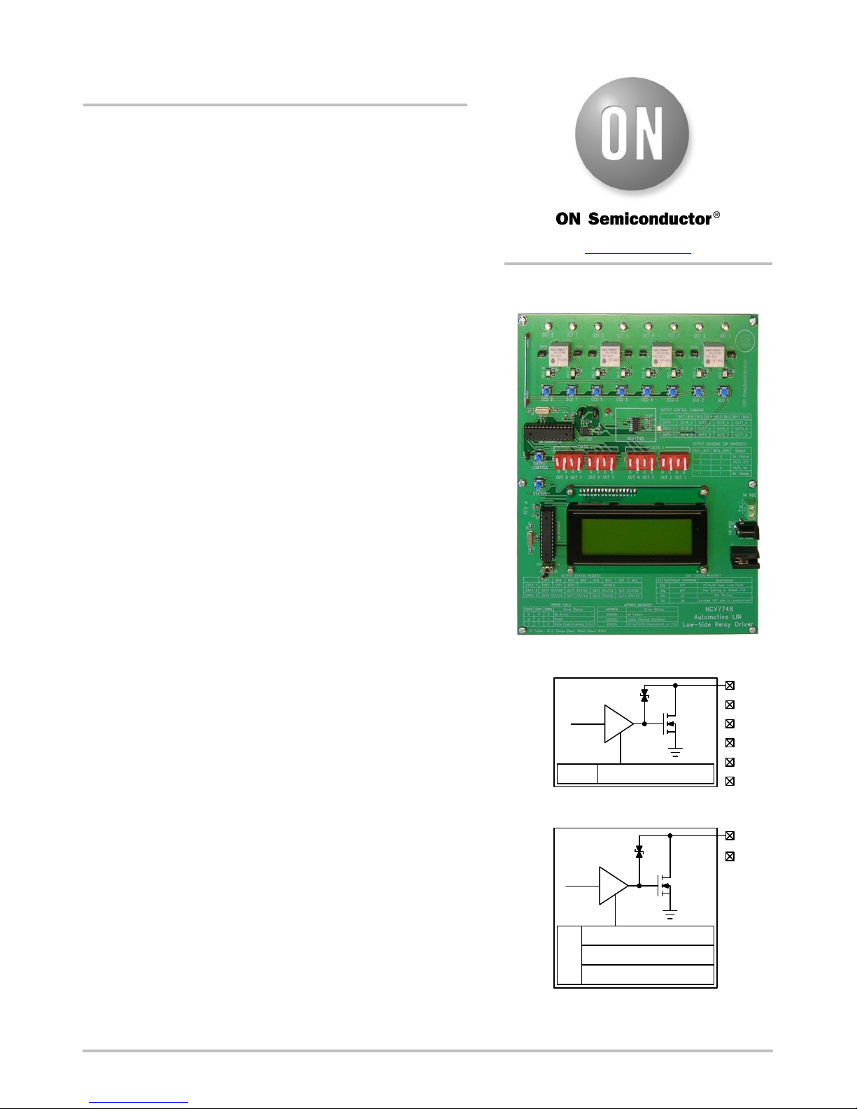
EVAL BOARD USER’S MANUAL
Figure 1. NCV7748 Evaluation Board
41 V
(Typ)
1.5 W
(Typ)
Over CurrentFault
Figure 2. 1.5 W Output Drivers
41 V
(Typ)
0.8 W
(Typ)
Thermal Shutdown
Over Current
Fault
Figure 3. 0.8 W Output Drivers
Open Load
OUT
OUT
OUT
OUT
OUT
OUT
OUT
OUT
© Semiconductor Components Industries, LLC, 2016
July, 2016 − Rev. 0
1 Publication Order Number:
EVBUM2484/D
Page 2
NCV7748GEVB
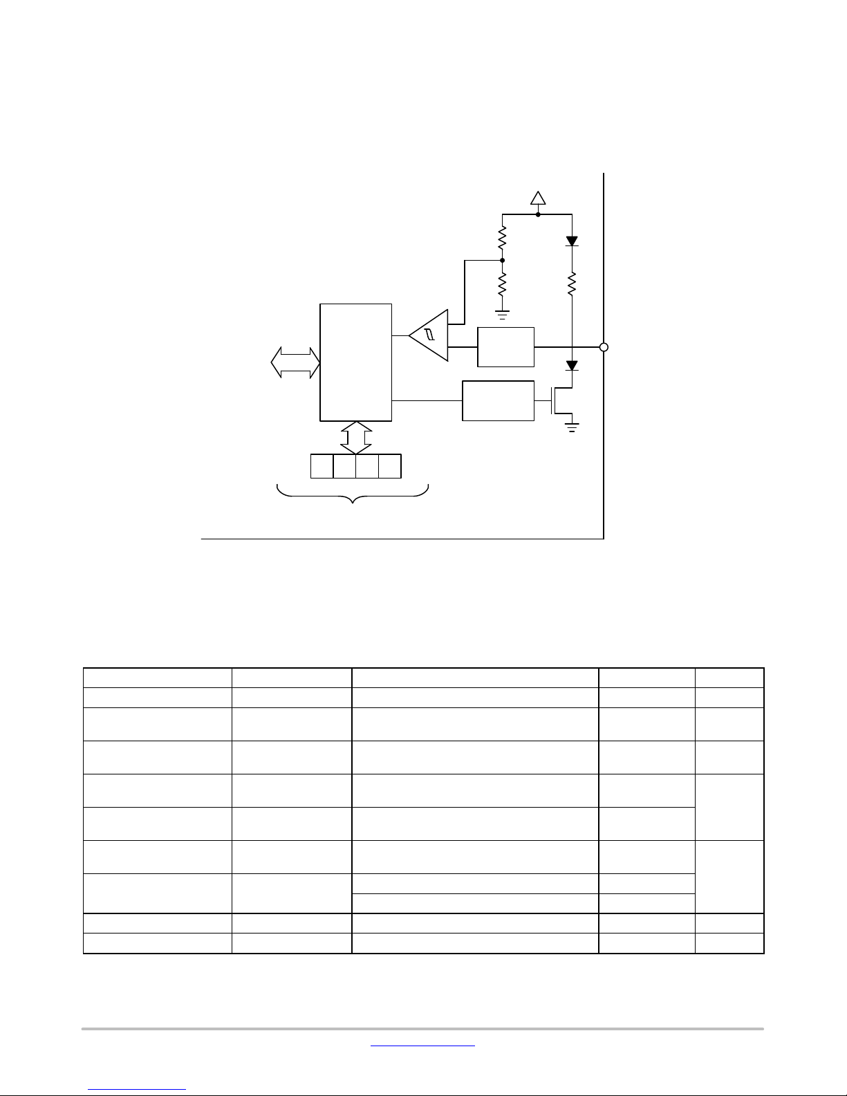
Communication
The NCV7748 utilizes a LIN protocol for all
communication. LIN is a single wire communication
network which utilizes a master/slave configuration. The
NCV7748 is the slave and receives its commands from an
To
Control
Block
LIN Address
LIN
Protocol
Handler
external master device and also reports on the same pin
(LIN) to the master device after a request is made. Figure 4
shows the basic LIN schematic. The LIN bus is driven high
through a 30 kW resistor in series with a diode and its read
capability is filtered to an internal RxD comparator.
VBB
30 kW
RxD
−
+
TxD
Filter
Slope
Control
LIN
From NAD Register
Figure 4. LIN Controller
A table (Table 1) of supported commands of the
NCV7748 is listed below from the NCP7744/D data sheet.
comprised of 4 outputs instead of the 8 outputs of the
NCV7748.
Note the NCV7744 reference is to a sister part which is
Table 1. SUPPORTED LIN COMMANDS
PID[7:0] Frame Type Description Data Length Spec
Depends on NAD Output Control Sets all outputs in one virtual node. 8 N/A
Depends on NAD Get Node ID Reads identity of prime device in virtual node.
Depends on Rconfig
and NAD
0x3C Targeted Reset
0x7D Targeted Reset
0x3C Read by Identifier
0x7D Read by Identifier
0x3C Broadcast Reset Re-initialization of all nodes. 8 J2602−1
0x3C Goto Sleep All devices enters Sleep Mode. 8 LIN2.2
Get Status Reads diagnostics of one device (LS driver).
Master Request
Slave Response
Master Request
Slave Response
(In frame slave Response)
(In frame slave Response)
Re-initialization of one virtual node.
This includes all devices on the virtual node.
Positive response by prime device. 8
Reads identity of device supplier. 8
Successfully processed request. 8
Slave could not process the request. 8
8 N/A
8 N/A
8
J2602−1
LIN2.2
www.onsemi.com
2
Page 3
NCV7748GEVB
The NCV7748GEVB is capable of demonstrating:
• Output Control
A one-way command which sets all outputs in one
virtual node (see NCP7744/D data sheet for virtual
node definition).
• Get Status
A two-way command which requests device
diagnostics and receives a response with an in-frame
response.
• Display of Sleep Mode
After timeout.
Practical setup limitations do not allow the display of Get
Node ID, Targeted Reset, Read by Identifier, Broadcast
Reset, and Goto Sleep on this board. A further enhanced
setup using enriched software is needed to display all device
features.
Table 2. MAXIMUM RATINGS
Rating Value Unit
Supply Voltage to Board (14VDC) (Using On-board NEC Relays) −0.3 to 16 V
Supply Voltage to Board (14 VDC) (Removing LOAD1−8 Jumpers) −0.3 to 40 V
TxD −0.3 to 5.25 V
RxD −0.3 to 5.25 V
LIN −40 to 40 V
Output Pin Voltage (OUT1− OUT8) (Removing LOAD1−8 Jumpers) Using External Loads −0.3 to 38 V
Junction Temperature (NCV7748) −40 to 150 °C
Temperature (Evaluation Board) −40 to 105 °C
Stresses exceeding those listed in the Maximum Ratings table may damage the device. If any of these limits are exceeded, device functionality
should not be assumed, damage may occur and reliability may be affected.
The operation of the NCV7748 evaluation board works as
a standalone presentation for the customer highlighting LIN
communication for turning on and off low-side drivers (both
1.5 W and 0.8 W). Dip switches provide the user
programmability for the Control Frame. Jumpers provide
convenient access to TxD, RxD, and the LIN pin which are
normally connected to the on-board microprocessor.
Jumpers are also included for use with external loads.
A jumper is included to maintain output control to avoid
going to sleep after the NCV7748 “Time to go to sleep”
electrical parameter. Pushbuttons are included for
implementing the user control of Output Control and Get
Status. Pushbuttons are also included to provide overcurrent
conditions (OCD) of the loads. A demo mode is provided via
a toggle switch.
The user must adhere to the absolute maximum ratings
when using off-board connections.
Table 3. RECOMMENDED BOARD OPERATING CONDITIONS
Rating Min Max Unit
External Supply Voltage (14VDC) − 16 V
Junction Temperature (NCV7748) −40 150 °C
Functional operation above the stresses listed in the Recommended Operating Ranges is not implied. Extended exposure to stresses beyond
the Recommended Operating Ranges limits may affect device reliability.
Table 4. PIN FUNCTION DESCRIPTION
Connector Pin Number Terminal Name Description
Power
Test Points
J12, J13 14 VDC Power Supply Input Voltage (14 V)
GND GND Ground
J1 LIN LIN Bus
J2−8, J11 LOAD 1−8 On-board Relay Disconnect
J9 OUTPUT CONTROL LIN Command for Output Control (Pushbutton Shorts to Ground)
J10 HEADER 16 Header for LCD Display
J14−J19 N/A Board Post Mount Holes
J20−J23 N/A LCD Display Post Mount Holes
J24 TxD NCV7321 TxD Input
J25 RxD NCV7321 RxD Output
www.onsemi.com
3
Page 4
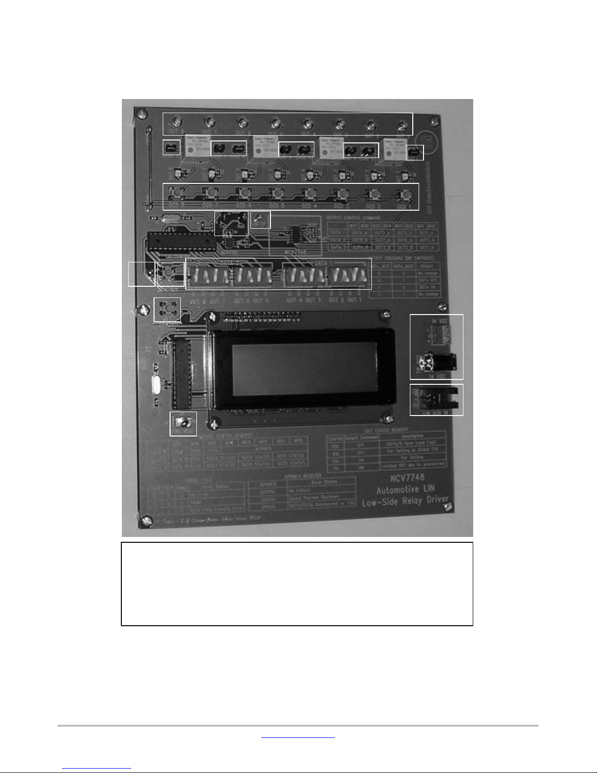
User Interface Locations
Figure 5 shows all the user interface locations. This lists
all the user options available on the evaluation board.
NCV7748GEVB
1
2
8
9
10
2
5
4
2
3
67
2
2
11
12
1. OUT1−8 External Post Connections
2. External Relay Jumpers
3. Overcurrent (OCD) Pushbuttons
4. TxD, RxD Jumpers
5. LIN Test Point
6. Output Control Command Input Data
7. Output Control Pushbutton
8. LOOP Jumper for Continuous Operation
without Four Second Timeout
9. Get Status Pushbutton
10. Demo Mode Toggle Switch
11. 14 VDC Power Supply Inputs
12. LIN Auxiliary Input
Figure 5. User Interface Locations
www.onsemi.com
4
Page 5

NCV7748GEVB
OPERATIONAL GUIDELINES
The material necessary to successfully use the evaluation
board is listed below.
• NCV7748 Evaluation Board
• 14 V Power Supply Capable of Drive 1 A
Configure the Board
Typical Board Configuration with On-board Components
1. Connect all jumpers on the board with the
exception of the LOOP jumper (J9) for output
control. This jumper is located directly next to the
OUTPUT CONTROL pushbutton.
2. Set the DEMO MODE toggle switch OFF.
Demo Mode
1. Configure the board as per above.
2. Connect the 14 V power supply.
3. Turn on the power supply.
4. The splash screen will be shown (see Figure 6).
5. Move the DEMO MODE toggle switch to the ON
position.
Figure 6. Splash Screen
At this point, the relays will individually sequence from
OUT1 to OUT8 and repeat. This is indicated on the board
with the illumination of the LEDs connected to the outputs
of the relays. Figure 7 shows the board when OUT2 is
illuminated. This will continue indefinitely. Switching the
demo mode toggle switch off, the sequence will continue
and stop on OUT8 until the NCV7748 device times out and
OUT8 will also turn off.
Figure 7. Sequencing Demo Mode
Normal Operation
1. Move the DEMO MODE toggle switch to the OFF
mode.
2. This sets the NCV7748 ready to receive LIN
commands from the on-board microprocessor.
3. Set the DIP switches using the OUTPUT
CONTROL COMMAND for DATA 1 and
DATA 2 for the targeted outputs and the OUTPUT
ENCODING for the output state. In this mode,
DATA 3 will always display all zeros.
4. Press the OUTPUT CONTROL pushbutton
(Figure 9) located to the left of the DIP switches.
5. The selected outputs will turn on.
NOTE: Figure 8 displays the setup for all 8
outputs to turn on.
NOTE: Figure 12 highlights the dip switches
settings and the resultant display of the settings.
All selected outputs will remain illuminated until
the NCV7748 sleep timer has expired. This is
indicative of no communication on the LIN bus.
When the sleep timer expires, all outputs will turn
off. When in sleep mode, a GET STATUS
command will display “Sleep Mode”. All 1’s are
displayed (Figure 10) because the bus is recessive
in sleep mode.
6. To circumvent the sleep timer and maintain
a continuous output state, connect the jumper
(LOOP) next to the OUTPUT CONTROL
pushbutton (see Figure 9). This will repeatedly
send LIN commands. As a result the device will
not go to sleep. DIP switch activity is allowed with
the loop jumper connected. This allows for real
time switching selection of the output drivers.
www.onsemi.com
5
Page 6

NCV7748GEVB
Output Control Command
DATA_1 OUT4_A OUT3_A OUT2_A OUT1_A
DATA_2 OUT8_A OUT7_A OUT6_A OUT5_A
DATA_3 OUT4_B OUT3_B OUT2_B OUT1_B
Bit7 Bit6 Bit5 Bit4 Bit3 Bit2 Bit1 Bit0
Figure 8. OUTPUT CONTROL DIP Switches
(All Outputs On)
Figure 9. OUTPUT CONTROL Button
Figure 10. Sleep Mode
Output Encoding (DIP Switches)
OUTx_A[1] OUTx_A[0] Output
0 0 No Change
0 1 OUT x Off
1 0 OUT x On
1 1 No Change
Figure 11. OUTPUT CONTROL and OUTPUT
ENCODING
Figure 12. OUTPUT CONTROL Display
www.onsemi.com
6
Page 7

NCV7748GEVB
GET STATUS
To retrieve the outputs status including the state of the
output and any information stored in the error field and
APPINFO registers, simply press the GET STATUS button
located directly below the OUTPUT CONTROL button.
Note, if you have the LOOP jumper connected, the GET
STATUS information will only be displayed while the
button is depressed. Remove the LOOP jumper if
a continuous display of error information is desired.
All zeros in the ERR and APPINFO register are indicative
of normal operation with no issues.
Errors which can be detected on this board include:
Figure 13. Byte Field Framing Error
ERR
1. No Error.
2. Reset. A reset error will be displayed with VBB
por.
3. Byte Field Framing Error. An error can be seen
here when there is conflict on the bus such as
when two opposing signals are sent from DEMO
MODE and OUTPUT CONTROL followed by
a GET STATUS command.
To see this error:
a. Put the toggle switch in demo mode.
b. While in demo mode, press the output
control pushbutton.
c. Release the output control pushbutton.
d. Leave demo mode using the toggle switch
before OUT8 turns on.
e. Press the Get Status pushbutton. Multiple
attempts may be required to see this result.
APPINFO
4. No Failure.
5. Global Thermal Shutdown*.
6. OUT4/OUT8 Overcurrent or Thermal Shutdown*.
a. Overcurrent setups are created with the
individual OCD (1−8) pushbuttons. Only
OUT4 and OUT8 are reported in the
APPINFO register by design.
b. Overcurrent is also reported in the output
status readout (Figure 14). This is a latched
off event. A successful turn-off command
must be sent before an output in an OCD
condition will turn back on.
*Thermal Shutdown events are not advised on this board due to the
potential damage.
Figure 14. Output Status and Error Reporting Decoding
Open Load
Open load conditions are reported in the status reporting
for OUT4 and OUT8. Jumpers labeled Load 1–Load 8 are
included on the board. Figure 14 shows how open load faults
are reported in the OUT STATUS READOUT. These are
reported in the output off state.
External LIN Communication
The NCV7748GEVB uses an NCV7321 LIN transceiver
for communication from the microprocessor to the LIN bus
pin of the NCV7748 device. Jumpers are include for the TxD
and RxD pins with and adjacent LIN connection pin
providing the user with flexibility for an external LIN based
master device.
Additionally an RJ11 connector provides an alternative
for a connection to the LIN bus with a connection to VBB,
and ground.
www.onsemi.com
7
Page 8

SCHEMATIC
NCV7748GEVB
Figure 15. Evaluation Board Schematic (1 of 2)
www.onsemi.com
8
Page 9

NCV7748GEVB
Figure 16. Evaluation Board Schematic (2 of 2)
www.onsemi.com
9
Page 10

PCB
NCV7748GEVB
Figure 17. Printed Circuit Board
www.onsemi.com
10
Page 11

NCV7748GEVB
BILL OF MATERIALS
Table 5. BILL OF MATERIALS OF NCV7748GEVB
Designator Qty. Description Value Tolerance Footprint Manufacturer
C1, C2,
C10, C11
C3, C4, C5,
C7, C8, C9,
C12, C13,
C14, C15
C6 1 5 V Regulator Output
C16 1 LIN Bus Capacitor 100 pF 5% 0805 KEMET C0805C101J5GACTU Yes
C17−C24 8 Output Capacitors
DN1 1 LIN Bus Protector − − SOT23 ON Semiconductor NUP1105LT1G Yes
D1−D8 8 Relay LEDs Red − PLCC2_LED VISHAY SEMI OPTO VLMS30K1L2−GS08 Yes
D9 1 Reverse Battery Diode MRA4003 − SMA_DIODE ON Semiconductor MRA4003T3G Yes
J1 1 RJ11 Right Angle Socket LIN Aux − FCI_87180_044LF MOLEX 432024101 Yes
J2−J9, J11,
J24, J25
J2−J9, J11,
J24, J25
J10 1 16 Pin Header for LCD
J12 1 2 Position Screw Terminal
J13 1 DC Jack VBB − PWRJACK CUI, INC PJ−102A Yes
LS1, LS2,
LS3, LS4
R9−R16 8 LED Resistors
R1, R2, R7,
R20
R3, R6 2 Oscillator Bias Resistors
R4, R5 2 NAD and CONF Program
R17 1 LIN Pull-up Resistor
R18 1 LCD Backlight Resistor
R19 1 Thumbwheel Potentiometer
SOCKET1,2 2 28 Pin DIP Sockets for
SW1−SW4 4 Output Command DIP
SW5 1 Demo Mode Switch − − MINITOGGLE MULTICOMP 2MS1T2B2M2RE Yes
SW6 1 Output Control Pushbutton − − SW_6x6_TACTILE TE CCONNECTIVITY
SW7 1 Get Status Pushbutton − − SW_6x6_TACTILE TE CCONNECTIVITY
SW8−SW15 8 OCD Pushbutttons − − SW_6x6_TACTILE TE CCONNECTIVITY
TP13−TP20 8 Off-board Load Turrets − − TURRET MIL−MAX 2501−2−00−44−00−00−07−0 Yes
TP21 1 LIN Bus Test Point − − TP KEYSTONE
TP22, TP23 2 GND Test Points − − TP KEYSTONE
U1 1 NCV7748 LIN Relay Driver − − SOIC14_N ON Semiconductor NCV7748D2R2G No
U2 1 NCV4274A 5 V Regulator − − DPAK3_SMD ON Semiconductor NCV4274ADT50RKG Yes
U3 1 7407 Open-collector Hex
U4 1 NCV7321 LIN Transceiver − − SOIC8_N ON Semiconductor NCV7321D11R2G No
4 Oscillator Load Capacitors 20 pF 5% 0805 KEMET C0805C200J5GACTU Yes
10 Bypass Capacitors
Capacitor
11 Jumper Posts 100 mil
11 Jumpers − − N/A SULLINS
4 Dual Automotive Relay 25A − EX2_RELAY KEMET NEC−TOKIN EX2−2U1S No
5 Pull-up Resistors
Spacing
Module
Block
Resistors
Arduinos
Switches
Buffer
0.1 mF
22 mF
0.01 mF
JUMPER − JMP 3M 961102−6404−AR Yes
− − SIP−16P SULLINS
VBB − MKDSN2 PHOENIX CONTACT 1729128 Yes
10 kW
10 kW
1MW
475 W
1kW
220 W
10 kW
− − DIP28 ON SHORE
− − DIP14 GRAYHILL 76STC04T No
− − SOIC14_N TEXAS
10% 0805 KEMET C0805C104K5RACTU Yes
20% 1206 KEMET C1206C226M4PAC7800 Yes
10% 0805 KEMET C0805C103K5RACTU Yes
CONNECTOR
SOLUTIONS
CONNECTOR
SOLUTIONS
1% 0805 VISHAY DALE CRCW080510K0FKEA Yes
1% 0805 VISHAY DALE CRCW080510K0FKEA Yes
1% 0805 VISHAY DALE CRCW08051M00FKEA Yes
1% 0805 VISHAY DALE CRCW0805475RFKEA Yes
1% 0805 VISHAY DALE CRCW08051K00FKEA Yes
1% 0805 VISHAY DALE CRCW0805220RFKEA Yes
20% 3352E_POT BOURNS INC 3352E−1−103LF Yes
TECHNOLOGY INC
ALCOSWITCH
ALCOSWITCH
ALCOSWITCH
ELECTRONICS
ELECTRONICS
INSTRUMENTS
Part
Number
QPC02SXGN−RC Yes
PRPC016SAAN−RC Yes
ED281DT Yes
1−1825910−0 Yes
1−1825910−0 Yes
1−1825910−0 Yes
5010 Yes
5010 Yes
SN7407DR Yes
Substitution
Allowed
www.onsemi.com
11
Page 12

NCV7748GEVB
P
al
Table 5. BILL OF MATERIALS OF NCV7748GEVB (continued)
Designator
Y1, Y2 2 16 MHz Microprocessor
LIN
Generator
LIN Decoder 1 Arduino-based
LCD 1 20 x 4 LCD Module − − N/A COFUFU LCM TM204A Yes
1 Arduino-based
Crystals
Microprocessor
Microprocessor
20 pF 30 ppm XTAL CTS−FREQUENCY
− − N/A ATMEL ATMEGA328P−PU No
− − N/A ATMEL ATMEGA328P−PU No
ManufacturerFootprintToleranceValueDescriptionQty.
CONTROLS
Part
Number
ATS16A Yes
Substitution
Allowed
ON Semiconductor and are trademarks of Semiconductor Components Industries, LLC dba ON Semiconductor or its subsidiaries in the United States and/or other countries.
ON Semiconductor owns the rights to a number of patents, trademarks, copyrights, trade secrets, and other intellectual property. A listing of ON Semiconductor ’s product/patent
coverage may be accessed at www.onsemi.com/site/pdf/Patent−Marking.pdf
ON Semiconductor makes no warranty, representation or guarantee regarding the suitability of its products for any particular purpose, nor does ON Semiconductor assume any liability
arising out of the application or use of any product or circuit, and specifically disclaims any and all liability, including without limitation special, consequential or incidental damages.
Buyer is responsible for its products and applications using ON Semiconductor products, including compliance with all laws, regulations and safety requirements or standards,
regardless of any support or applications information provided by ON Semiconductor. “Typical” parameters which may be provided in ON Semiconductor data sheets and/or
specifications can and do vary in different applications and actual performance may vary over time. All operating parameters, including “Typicals” must be validated for each customer
application by customer’s technical experts. ON Semiconductor does not convey any license under its patent rights nor the rights of others. ON Semiconductor products are not
designed, intended, or authorized for use as a critical component in life support systems or any FDA Class 3 medical devices or medical devices with a same or similar classification
in a foreign jurisdiction or any devices intended for implantation in the human body. Should Buyer purchase or use ON Semiconductor products for any such unintended or unauthorized
application, Buyer shall indemnify and hold ON Semiconductor and its officers, employees, subsidiaries, affiliates, and distributors harmless against all claims, costs, damages, and
expenses, and reasonable attorney fees arising out of, directly or indirectly, any claim of personal injury or death associated with such unintended or unauthorized use, even if such
claim alleges that ON Semiconductor was negligent regarding the design or manufacture of the part. ON Semiconductor is an Equal Opportunity/Affirmative Action Employer. This
literature is subject to all applicable copyright laws and is not for resale in any manner.
UBLICATION ORDERING INFORMATION
LITERATURE FULFILLMENT:
Literature Distribution Center for ON Semiconductor
19521 E. 32nd Pkwy, Aurora, Colorado 80011 USA
Phone: 303−675−2175 or 800−344−3860 Toll Free USA/Canada
Fax: 303−675−2176 or 800−344−3867 Toll Free USA/Canada
Email: orderlit@onsemi.com
. ON Semiconductor reserves the right to make changes without further notice to any products herein.
N. American Technical Support: 800−282−9855 Toll Free
USA/Canada
Europe, Middle East and Africa Technical Support:
Phone: 421 33 790 2910
Japan Customer Focus Center
Phone: 81−3−5817−1050
ON Semiconductor Website: www.onsemi.com
Order Literature: http://www.onsemi.com/orderlit
For additional information, please contact your loc
Sales Representative
www.onsemi.com
12
EVBUM2484/D
 Loading...