

Page 1
Triple Half-Bridge Driver
with SPI Control
NCV7703C
The NCV7703C is a fully protected Triple Half−Bridge Driver
designed specifically for automotive and industrial motion control
applications. The three half−bridge drivers have independent control.
This allows for high side, low side, and H−Bridge control. H−Bridge
control provides forward, reverse, brake, and high impedance states
(with EN = 0). The drivers are controlled via a standard Serial
Peripheral Interface (SPI).
Features
• Ultra Low Quiescent Current in Sleep Mode, 1 mA for V
• 3 High−Side and 3 Low−Side Drivers Connected as Half−Bridges
• Internal Free−Wheeling Diodes
• Configurable as H−Bridge Drivers
• 500 mA (typ), 1.1 A (max) Drivers
• R
= 0.8 W (typ), 1.7 W (max)
DS(on)
• 5 MHz SPI Control with Daisy Chain Capability
• Compliance with 5 V and 3.3 V Systems
• Overvoltage and Undervoltage Lockout
• Fault Reporting
• 1.45 A Overcurrent Threshold Detection
• 3 A Current Limit
• Shoot−Through Attempt Detection
• Overtemperature Warning and Protection Levels
• Internally Fused Leads in SOIC−14 for Better Thermal Performance
• ESD Protection up to 6 kV
• These are Pb−Free Devices
and V
S
CC
14
www.onsemi.com
MARKING
DIAGRAM
14
SOIC−14
D2 SUFFIX
1
CASE 751A
NCV7703C = Specific Device Code
A = Assembly Location
WL = Wafer Lot
Y = Year
WW = Work Week
G = Pb−Free Package
PIN CONNECTIONS
GND
OUT3
V
S
CSB
SI
SCLK
GND
NCV7703CG
AWLYWW
1
GND
OUT1
OUT2
V
CC
EN
SO
GND
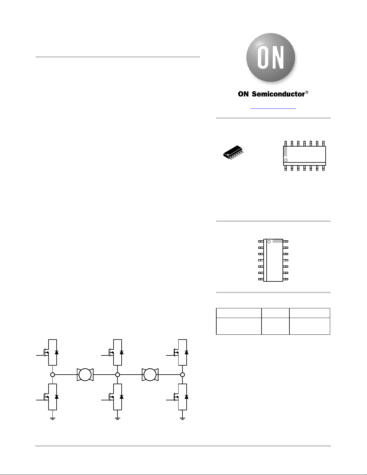
Typical Applications
• Automotive
• Industrial
• DC Motor Management
V
S
OUT1 OUT2
© Semiconductor Components Industries, LLC, 2016
March, 2021 − Rev. 5
M M
Figure 1. Cascaded Application
V
ORDERING INFORMATION
Device Package Shipping†
NCV7703CD2R2G SOIC−14
S
V
S
OUT3
1 Publication Order Number:
†For information on tape and reel specifications,
including part orientation and tape sizes, please
refer to our Tape and Reel Packaging Specifications
Brochure, BRD8011/D.
(Pb−Free)
2500 /
Tape & Reel
NCV7703C/D
Page 2
NCV7703C
V
S
EN
V
CC
SO
SCLK
CSB
V
POR
ENABLE OSC
Reference
& Bias
Fault
Detect
clk
S
clk
Charge
Pump
Control
Logic
Channel Enable
Waveshaping
V
V
S
High−Side
Driver
S
OUT1
Low−Side
Driver
Waveshaping
Under−Load
DRIVE 1
SI
SPI
16 Bit
Logic
and
Overcurrent
Fault
Thermal
Warning/Shutdown
Latch
V
S
clk
Channel Enable
DRIVE 2
OUT2
Fault
V
V
S
S
Undervoltage
Lockout
Overvoltage
V
S
clk
Channel Enable
Fault
DRIVE 3
OUT3
Lockout
Figure 2. Block Diagram
GND
PACKAGE PIN DESCRIPTION
Pin #
1 GND* Ground. Connect all grounds together.
2 OUT3 Half Bridge Output 3.
3 V
4 CSB Chip Select Bar. Active low serial port operation.
5 SI Serial Input
6 SCLK Serial Clock
7 GND* Ground. Connect all grounds together.
8 GND* Ground. Connect all grounds together.
9 SO Serial Output
10 EN Enable. Logic high wakes the IC up from a sleep mode.
11 V
12 OUT2 Half Bridge Output 2.
13 OUT1 Half Bridge Output 1.
14 GND* Ground. Connect all grounds together.
*Pins 1, 7, 8, and 14 are internally shorted together. It is recommended to also short these pins externally.
Symbol Description
S
CC
Power Supply input for the output drivers and internal supply voltage.
Power supply input for internal logic.
www.onsemi.com
2
Page 3
22 mF
C1
WDI
Wake Up
RESET
Vout
NCV7703C
NCV8518
Delay
120k
GND
D1*
1N4001
D2**
ENABLE
VBAT
10 mF
+
−
V
CC
EN
CSB
microprocessor
GND
SI
SCLK
SO
GND
GND
GND
GND
NCV7703C
* D1 optional. For use where reverse battery protection is required.
** D2 optional. For use where load dump exceeds 40V.
*** C2−C4, Recommended for EMC performance.
Figure 3. Application Circuit
V
S
OUT1
C2***
M
OUT2
M
OUT3
10 nF
C3***
10 nF
C4***
10 nF
www.onsemi.com
3
Page 4
NCV7703C
MAXIMUM RATINGS
Rating Value Unit
Power Supply Voltage (VS)
(DC)
(AC), t < 500 ms, Ivs > −2 A
−0.3 to 40
−1
Output Pin OUTx
(DC)
(AC), t < 500 ms, IOUTx > −2 A
Pin Voltage
(Logic Input pins, SI, SCLK, CSB, SO, EN, V
CC
)
−0.3 to 40
−1
−0.3 to 5.5 V
Output Current (OUTx)
(DC)
(AC) (50 ms pulse, 1 s period)
Electrostatic Discharge, Human Body Model,
, OUT1, OUT2, OUT3 (Note 3)
V
S
Electrostatic Discharge, Human Body Model,
−2.0 to 2.0
−5.0 to 5.0
6 kV
2 kV
all other pins (Note 3)
Electrostatic Discharge, Machine Model,
, OUT1, OUT2, OUT3 (Note 3)
V
S
Electrostatic Discharge, Machine Model,
300 V
200 V
all other pins (Note 3)
Operating Junction Temperature −40 to 150 °C
Storage Temperature Range −55 to 150 °C
Moisture Sensitivity Level (MAX 260°C Processing) MSL3 −
Stresses exceeding those listed in the Maximum Ratings table may damage the device. If any of these limits are exceeded, device functionality
should not be assumed, damage may occur and reliability may be affected.
V
V
A
Thermal Parameters
Test Conditions (Typical Value) Unit
14 Pin Fused SOIC Package min−pad board
(Note 1)
Junction−to−Lead (psi−JL8, Y
Junction−to−Ambient (R
1. 1−oz copper, 67 mm2 copper area, 0.062″ thick FR4.
2. 1−oz copper, 645 mm
q
2
) or Pins 1, 7, 8, 14
JL8
, qJA)
JA
copper area, 0.062″ thick FR4.
23 22
122 83
3. This device series incorporates ESD protection and is characterized by the following methods:
ESD HBM according to AEC−Q100−002 (EIA/JESD22−A114)
ESD MM according to AEC−Q100−003 (EIA/JESD22−A115)
1″ pad board
(Note 2)
°C/W
°C/W
www.onsemi.com
4
Page 5
NCV7703C
ELECTRICAL CHARACTERISTICS
(−40°C ≤ TJ ≤ 150°C, 5.5 V ≤ VS ≤ 40 V, 3.15 V ≤ VCC ≤ 5.25 V, EN = VCC, unless otherwise specified)
Characteristic Conditions Min Typ Max Unit
GENERAL
Supply Current (V
Sleep Mode (Note 5)
)
S
VS = 13.2 V, OUTx = 0 V
EN = SI = SCLK = 0 V, CSB = V
0 V < VCC < 5.25 V
(T
= −40°C to 85°C)
J
CC
−
1.0
5.0
mA
= 13.2 V, OUTx = 0 V
V
S
EN = SI = SCLK = 0 V, CSB = V
CC
−
−
2.0
0 V < VCC < 5.25 V, TJ = 25°C
Supply Current (VS)
Active Mode
Supply Current (VCC)
Sleep Mode (Note 6)
Supply Current (VCC)
EN = VCC, 5.5 V < VS < 35 V
No Load
VCC = CSB, EN = SI = SCLK = 0 V
= −40°C to 85°C)
(T
J
EN = V
CC
− 2.0 4.0 mA
− 0.1 2.5
− 1.5 3.0 mA
Active Mode
VCC Power−On−Reset Threshold − 2.55 2.90 V
VS Undervoltage Detection Threshold
Hysteresis
VS Overvoltage Detection Threshold
Hysteresis
Thermal Warning (Note 4) Threshold
Hysteresis
Thermal Shutdown (Note 4) Threshold
Hysteresis
Ratio of Thermal Shutdown to Thermal
VS decreasing 3.7
100
VS increasing 33.0
1.0
120
−
155
−
1.05 1.20 − °C/°C
4.1
365
36.5
2.5
140
20
175
30
4.5
450
40.0
4.0
170
−
195
−
Warning temperature (Note 4)
OUTPUTS
Output R
Output R
(Source) I
DS(on)
(Sink) I
DS(on)
Source Leakage Current
Sum of I(OUTx) x = 1, 2, 3
= −500 mA − − 1.7
out
= 500 mA − − 1.7
out
OUTx = 0 V, VS = 40 V, EN = 0 V
CSB = V
CC
−5.0
−
−
0 V < VCC < 5.25 V
Sum(I(OUTx)
mA
mA
V
mV
V
°C
°C
W
W
mA
OUTx = 0 V, V
CSB = V
= 40 V, EN = 0 V
S
CC
−1.0
−
−
0 V < VCC < 5.25 V, TJ = 25°C
Sum(I(OUTx)
Sink Leakage Current OUTx = VS = 40 V, EN = 0 V
CSB = V
CC
−
−
300
mA
0 V < VCC < 5.25 V
OUTx = V
CSB = V
= 13.2 V, EN = 0 V
S
CC
−
−
10
0 V < VCC < 5.25 V, TJ = 25°C
Product parametric performance is indicated in the Electrical Characteristics for the listed test conditions, unless otherwise noted. Product
performance may not be indicated by the Electrical Characteristics if operated under different conditions.
4. Thermal characteristics are not subject to production test
5. For temperatures above 85°C, refer to Figure 6.
6. For temperatures above 85°C, refer to Figure 7.
7. Current limit is active with and without overcurrent detection.
www.onsemi.com
5
Page 6
NCV7703C
ELECTRICAL CHARACTERISTICS
(−40°C ≤ TJ ≤ 150°C, 5.5 V ≤ VS ≤ 40 V, 3.15 V ≤ VCC ≤ 5.25 V, EN = VCC, unless otherwise specified)
Characteristic UnitMaxTypMinConditions
OUTPUTS
Under Load Detection Threshold Source
Power Transistor Body Diode Forward Voltage If = 500 mA − 0.9 1.3 V
OVERCURRENT
Overcurrent Shutdown Threshold (OUTHx)
Overcurrent Shutdown Threshold (OUTLx) VCC = 5 V, Vs = 13.2 V 1.1 1.45 2.0 A
CURRENT LIMIT (Note 7)
Current Limit (OUTHx)
Current Limit (OUTLx) VCC = 5 V, Vs = 13.2 V,
Product parametric performance is indicated in the Electrical Characteristics for the listed test conditions, unless otherwise noted. Product
performance may not be indicated by the Electrical Characteristics if operated under different conditions.
4. Thermal characteristics are not subject to production test
5. For temperatures above 85°C, refer to Figure 6.
6. For temperatures above 85°C, refer to Figure 7.
7. Current limit is active with and without overcurrent detection.
Sink
VCC = 5 V, Vs = 13.2 V −2.0 −1.45 −1.1 A
VCC = 5 V, Vs = 13.2 V
−17
2.0
−5.0 −3.0 −2.0
2.0 3.0 5.0
−7.0
7.0
−2.0
17
mA
A
A
www.onsemi.com
6
Page 7
NCV7703C
ELECTRICAL CHARACTERISTICS
(−40°C ≤ TJ ≤ 150°C, 5.5 V ≤ VS ≤ 40 V, 3.15 V ≤ VCC ≤ 5.25 V, EN = VCC, unless otherwise specified)
Characteristic Symbol Conditions Min Typ Max Unit
LOGIC INPUTS (EN, SI, SCLK, CSB)
Input Threshold
High
Low
2.0
−
−
−
−
0.8
Input Hysteresis (EN, SI, SCLK, CSB) 100 400 800 mV
Pulldown Resistance (EN, SI, SCLK) EN = SI = SCLK = V
CC
50 125 250
Pullup Resistance (CSB) CSB = 0 V 50 125 250
Input Capacitance (Note 8) − 10 15 pF
LOGIC OUTPUT (SO)
I
Output High
Output Low I
Tri−state Leakage CSB = VCC, 0 V v SO v V
Tri−state Input Capacitance (Note 8) CSB = V
= 1 mA VCC – 1.0 VCC – 0.7 − V
out
= −1.6 mA − 0.2 0.4 V
out
CC
CC
−10 − 10
− 10 15 pF
TIMING SPECIFICATIONS
Under Load Detection Delay Time
200 350 600
Overcurrent Shutdown Delay Time VCC = 5 V, Vs = 13.2 V,
High Side Turn On Time ThsOn
High Side Turn Off Time ThsOff
Low Side Turn On Time TlsOn
Low Side Turn Off Time TlsOff
High Side Rise Time ThsTr
High Side Fall Time ThsTf
Low Side Rise Time TlsTr
Low Side Fall Time TlsTf
Bit13 = 0
Bit13 = 1
VS = 13.2 V, R
VS = 13.2 V, R
VS = 13.2 V, R
VS = 13.2 V, R
VS = 13.2 V, R
VS = 13.2 V, R
VS = 13.2 V, R
VS = 13.2 V, R
load
load
load
load
load
load
load
load
= 25 W
= 25 W
= 25 W
= 25 W
= 25 W
= 25 W
= 25 W
= 25 W
80
10
200
25
400
− 7.5 15
− 3.0 6.0
− 6.5 15
− 3.0 6.0
− 5.0 10
− 2.0 5.0
− 1.0 3.0
− 1.0 3.0
50
NonOverlap Time ThsOffLsOn High Side Turn Off to Low Side Turn On 1.0 − −
NonOverlap Time TlsOffHsOn Low Side Turn Off to High Side Turn On 1.0 − −
Product parametric performance is indicated in the Electrical Characteristics for the listed test conditions, unless otherwise noted. Product
performance may not be indicated by the Electrical Characteristics if operated under different conditions.
8. Not production tested.
V
kW
kW
mA
ms
ms
ms
ms
ms
ms
ms
ms
ms
ms
ms
ms
ms
www.onsemi.com
7
Page 8

NCV7703C
ELECTRICAL CHARACTERISTICS
(−40°C ≤ TJ ≤ 150°C, 5.5 V ≤ VS ≤ 40 V, 3.15 V ≤ VCC ≤ 5.25 V, EN = VCC, unless otherwise specified)
Characteristic Conditions Symbol Min Typ Max Unit
SERIAL PERIPHERAL INTERFACE (VCC = 5 V)
SCLK Frequency
SCLK Clock Period VCC = 5 V
SCLK High Time TCLKH 85 − − ns
SCLK Low Time TCLKL 85 − − ns
SCLK Setup Time TCLKSU1
SI Setup Time TISU 50 − − ns
SI Hold Time TIHT 50 − − ns
CSB Setup Time TCSBSU1
CSB High Time (Note 10) TCSBHT 5.0 − −
SO enable after CSB falling edge TSOCSBF − − 50 ns
SO disable after CSB rising edge TSOCSBR − − 50 ns
SO Rise Time (10% to 90%) C
SO Fall Time (90% to 10%) C
SO Valid Time (Note 9) SCLK High to SO 50% TSOV − 50 100 ns
Product parametric performance is indicated in the Electrical Characteristics for the listed test conditions, unless otherwise noted. Product
performance may not be indicated by the Electrical Characteristics if operated under different conditions.
9. Not tested in production
10.This is the minimum time the user must wait between SPI commands.
V
= 3.3 V
CC
= 40 pF − − 10 25 ns
load
= 40 pF − − 10 25 ns
load
− − − 5.0 MHz
− 200
TCLKSU2
TSSBSU2
500
85
85
100
100
−
−
−
−
−
−
−
−
−
−
−
−
ns
ns
ns
ms
www.onsemi.com
8
Page 9

NCV7703C
CHARACTERISTIC TIMING DIAGRAMS
TlsTr
TlsOff
90%
50%
LS Turn OFF
HS Turn ON
CSB
LS Turn On
HS Turn Off
50%
10%
TlsOffHsOn
ThsOn
TlsOn
90%
90%
50%
10%
ThsTr
TlsTf
90%
50%
10%
ThsOffLsOn
CSB
50%
10%
ThsTf
50%
ThsOff
Figure 4. Detailed Driver Timing
www.onsemi.com
9
Page 10

NCV7703C
CSB
SCLK
50%
TCSBSU1
TCLKSU1
CSB
TCLKSU2
50% 50% 50%50% 50% 50%
TCLKH TCLKL
50% 50%
TCSBHT
50%50%
TCSBSU2
SI
SCLK
SO
SO
50% 50%
50%
50% 50%
TSOCSBF
50% 50%
TSOV
TISU
Figure 5. SPI Timing Diagram
TSOCSBR
TIHT
www.onsemi.com
10
Page 11

NCV7703C
7.0
6.0
5.0
4.0
3.0
2.0
SLEEP CURRENT (mA)
S
V
1.0
0
VS = 13.2 V
VCC = 0 V to 5.25 V
100806040200−20−40
TJ, TEMPERATURE (°C)
120
Figure 6. VS Sleep Supply Current vs. Temperature
140 160
4.0
3.5
3.0
2.5
2.0
1.5
SLEEP CURRENT (mA)
1.0
CC
V
0.5
0
VS = 5.25 V
100806040200−20−40
TJ, TEMPERATURE (°C)
120
140 160
Figure 7. VCC Sleep Supply Current vs. Temperature
www.onsemi.com
11
Page 12

140
120
100
NCV7703C
TYPICAL CHARACTERISTICS
1 oz Cu
1000
100
R(t) (°C/W)
0.1
10
(°C/W)
JA
q
80
60
40
20
0
2 oz Cu
7006005004003002001000
COPPER HEAT SPREADING AREA (mm2)
800
Figure 8. qJA vs. Copper Spreader Area,
14 Lead SON (fused leads)
Cu Area = 100 mm2 1.0 oz
200 mm2 1.0 oz
300 mm2 1.0 oz
1
400 mm2 1.0 oz
500 mm2 1.0 oz
0.01
140
120
100
R(t) (°C/W)
80
60
40
20
0.00010.00001
TIME (sec)
10001001010.10.010.0010.000001
Figure 9. Transient Thermal Response to a
Single Pulse 1 oz Copper (Log−Log)
Cu Area = 100 mm2 1.0 oz
200 mm2 1.0 oz
300 mm2 1.0 oz
400 mm2 1.0 oz
500 mm2 1.0 oz
0
0.00010.00001
TIME (sec)
10001001010.10.010.0010.000001
Figure 10. Transient Thermal Response to a
Single Pulse 1 oz Copper (Semi−Log)
www.onsemi.com
12
Page 13

NCV7703C
SPI Communication
Standard 16−bit communication has been implemented to
this IC to turn drivers on/off, and to report faults. (See
Figure 12). The LSB (Least Significant Bit) is clocked in
first.
Communication is Implemented as Follows:
1. CSB goes low to allow serial data transfer.
2. A 16 bit word is clocked (SCLK) into the SI
(Serial Input) pin.
3. CSB goes high to transfer the clocked in
information to the data registers.
NOTE: SO is tristate when CSB is high.
Frame detection starts
after the CSB falling edge
and the SCLK rising edge.
CSB
SCLK
SI
nternal Counter
SRR OUTL1 XOUTH1 OUTL2 OUTH2 OUTL3 OUTH3
12345 678
Figure 11. Frame Detection
Frame Detection
Input word integrity (SI) is evaluated by the use of a frame
consistency check. The word frame length is compared to an
h x 16 bit acceptable word length before the data is latched
into the input register. This guarantees the proper word
length has been imported and allows for daisy chain
operation applications.
The frame length detector is enabled with the CSB falling
edge and the SCLK rising edge.
SCLK must be low during the CSB rising edge. The fault
register is cleared with a valid frame detection. Existing
faults are re−latched after the fault filter time.
Frame detection mode ends with
CSB rising edge.
ULDSDXXXX OCDX OVLO
9 1011 12 1314 1516
Valid 16 bits shown
CSB
SI
SCLK
SO
SRR OUTL1 OUTH1 OUTL2 OUTH2 OUTL3 OUTH3 X X X X X X OCD ULDSD OVLO
TW OUTL1 OUTH1 OUTL2 OUTH2 OUTL3 OUTH3 X X X X X STA OCDR ULDR PSF
Figure 12. SPI Communication Frame Format
Table 1 defines the programming bits and diagnostic bits.
Figure 12 displays the timing diagram associated with
Table 1. Fault information is sequentially clocked out the
SO pin of the NCV7703C as programming information is
clocked into the SI pin of the device. Daisy chain
communication between SPI compatible IC’s is possible by
connection of the Serial Output pin (SO) to the input of the
sequential IC (SI) (Reference the Daisy Chain Section).
www.onsemi.com
13
Page 14

NCV7703C
Table 1. SPI BIT DESCRIPTION
Input Data Output Data
Bit Number Bit Description Bit Status Bit Number Bit Description Bit Status
15 Over Voltage Lock Out
Control (OVLO)
14 Under Load Detection Shut
Down Control (ULDSD)
13 Over Current Detection Shut
Down Control (OCD)
12 Not Used 12 Shoot−Through Attempt
11 Not Used 11 Not Used
10 Not Used 10 Not Used
9 Not Used 9 Not Used
8 Not Used 8 Not Used
7 Not Used 7 Not Used
6 OUTH3
5 OUTL3
4 OUTH2
3 OUTL2
2 OUTH1
1 OUTL1
0 Status Register Reset (SRR)
0 = Disable
1 = Enable 1 = Fault
0 = Disable
1 = Enable 1 = Fault
0 = 200 msec
1 = 25 msec
0 = Off
1 = On 1 = On
0 = Off
1 = On 1 = On
0 = Off
1 = On 1 = On
0 = Off
1 = On 1 = On
0 = Off
1 = On 1 = On
0 = Off
1 = On 1 = On
0 = No Reset
1 = Reset 1 = In TW
15 VS Power Supply Fail Signal
(PSF for OVLO or UVLO)
14 Under Load Detection Reporting
Signal (ULDR)
13 Over Current Detection
Reporting Signal (OCDR)
(STA)
6 OUTH3
5 OUTL3
4 OUTH2
3 OUTL2
2 OUTH1
1 OUTL1
0 Thermal Warning (TW)
0 = No Fault
0 = No Fault
0 = No Fault
1 = Fault
0 = No Attempt
1 = Attempt
0 = Off
0 = Off
0 = Off
0 = Off
0 = Off
0 = Off
0 = Not in TW
DETAILED OPERATING DESCRIPTION
General
The NCV7703C Triple Half Bridge Driver provides drive
capability for 3 Half−Bridge configurations. Each output
drive is characterized for a 500 mA load and has a typical
1.4 A surge capability. Strict adherence to integrated circuit
die temperature is necessary, with a maximum die
temperature of 150°C. This may limit the number of drivers
enabled at one time. Output drive control and fault reporting
are handled via the SPI (Serial Peripheral Interface) port.
An Enable function (EN) provides a low quiescent sleep
current mode when the device is not being utilized. A pull
down is provided on the EN, SI and SCLK inputs to ensure
they default to a low state in the event of a severed input
signal. A pull−up is provided on the CSB input disabling SPI
communication in the event of an open CSB input.
www.onsemi.com
Power Up/Down Control
A feature incorporated in the IC is an under voltage
lockout circuit that prevents the output drivers from turning
on unintentionally. V
and VS are monitored for
CC
undervoltage conditions supporting a smooth turn−on
transition. All drivers are initialized in the off (high
impedance) condition, and will remain off during a V
V
undervoltage condition. This allows power up
S
sequencing of V
, and VS up to the user. Once VCC is above
CC
the Power−On−Reset threshold, SPI communication can
begin regardless of the voltage on V
. The VS supply input
S
does not ever affect the SPI logic. However, drivers will
remain off if V
in both V
is in an undervoltage condition. Hysteresis
S
and VS circuits results in glitch free operation
CC
during power up/down.
14
CC
or
Page 15

NCV7703C
Overvoltage Shutdown (Table 2)
Overvoltage lockout circuitry monitors the voltage on the
V
pin. The response to an overvoltage condition is selected
S
by SPI input bit 15. PSF output bit 15 is set when a V
overvoltage condition exists. If input bit 15 (OVLO) is set
Table 2. INPUT BIT 15, OVERVOLTAGE LOCK OUT (OVLO) SHUT DOWN
OVLO Input
Bit 15
0 0 0 Unchanged
0 1 1 (Need SRR to reset) Unchanged
1 0 0 Unchanged
1 1 1 (Need SRR to reset) All Outputs Shut Off (Remain off until VS is out of OVLO)
H−Bridge Driver Configuration
VS OVLO
Condition
Output Data Bit 15 Power
Supply Fail (PSF) Status
The NCV7703C has the flexibility of controlling each half
bridge driver independently. This allows for high side, low
side and H−bridge control. H−bridge control provides
forward, reverse, brake and high impedance states.
Overvoltage Clamping − Driving Inductive Loads
Each output is internally clamped to ground and VS by
internal freewheeling diodes. The diodes have ratings that
complement the FETs they protect. A flyback event from
driving an inductive load causes the voltage on the output to
rise up. Once the voltage rises higher than VS by a diode
voltage (body diode of the high−side driver), the energy in
the inductor will dissipate through the diode to VS. If a
reverse battery diode is used in the system, care must be
taken to insure the power supply capacitor is sufficient to
dampen any increase in voltage to VS caused by the current
flow through the body diode so that it is below 40 V.
Negative transients will momentarily occur when a
to “1”, all outputs will turn off during this overvoltage
condition. Turn On/Off status is maintained in the logic
circuitry, so that when proper input voltage level is
reestablished, the programmed outputs will turn back on.
S
The PSF output bit is reset with SRR = 1.
OUTx Status
Detection shutdown protects the device during current limit
because the Overcurrent threshold is below the Current
Limit threshold. The Overcurrent Detection Shutdown
Control Timer is initiated at the Overcurrent Shutdown
Threshold which starts before the Current Limit is reached.
Note: High currents will cause a rise in die temperature.
Devices will not be allowed to turn on if the die temperature
exceeds the thermal shutdown temperature.
Shoot−Through Attempt
The NCV7703C provides detection for attempting to turn
on common drivers of the same channel (OUTL1&OUTH1,
OUTL2&OUTH2, OUTL3&OUTH3) simultaneously. An
attempt to turn on common drivers if allowed would result
in a high current event from VS to GND. Any attempt to
create this setup is recorded in bit 12 of the output data and
forces the common high−side and low−side driver to an off
state. The STA output bit is reset with SRR = 1. The STA bit
must be cleared before an affected driver can turn on.
high−side driver driving an inductive load is turned off. This
will be clamped by an internal diode from the output pin
(OUT1 or OUT2) to the IC ground.
Overcurrent Shutdown
Effected outputs will turn off when the Overcurrent
Shutdown Threshold has been breached for the Overcurrent
Current Limit
OUTx current is limited per the Current Limit electrical
parameter for each driver. The magnitude of the current has
a minimum specification of 2 A at V
= 5 V and Vs =
CC
13.2 V. The output is protected for high power conditions
during Current Limit by thermal shutdown and the
Overcurrent Detection shutdown function. Overcurrent
Shutdown Delay Time. The respective OCDR status bit will
be set to a “1” and the driver will latch off. The driver can
only be turned back on via the SPI port with a SPI command
that includes an SRR = 1.
Note: High currents will cause a rise in die temperature.
Devices will not be allowed to turn on if the die temperature
exceeds the thermal shutdown temperature.
Table 3. OVERCURRENT DETECTION SHUT DOWN
OCD Input
Bit 13
0 0 0 Unchanged 3 A
0 1 1 (Need SRR to reset)
1 0 0 Unchanged 3 A
1 1 1 (Need SRR to reset)
OUTx OCD
Condition
Output Data Bit 13 Over
Current Detect (OCDR) Status
www.onsemi.com
OUTx Status
OUTx Latches off after 200 ms
(Need SRR to reset)
OUTx Latches Off After 25 ms
(Need SRR to reset)
15
Current Limit
of all Drivers
3 A
3 A
Page 16

NCV7703C
Overcurrent Detection Shut Down Control Timer
There are two protection mechanisms for output current,
overcurrent and current limit.
1. Current limit − Always active with a typical
threshold of 3 A (typ).
2. Overcurrent Detection − Selectable shutdown time
via Bit 13 with a 1.45 A (typ) threshold.
Figure 13 shows the typical performance of a part which
has exceeded the 1.45 A (typ) Overcurrent Detection
threshold and started the shutdown control timer. When Bit
13 = 1, the shutdown time is 25 msec (typ). When Bit 13 =
0, the shutdown time is 200 msec (typ).
(Current Limit) 3 A
(Overcurrent
Detection)
(Current Limit) 3 A
(Overcurrent
Detection)
1.45 A
OUTx Current
Bit13 = 1
1.45 A
OUTx Current
Bit13 = 0
25 msec (typ)
Once an Overcurrent Shutdown Delay Time event has
been detected by the NCV7703C, the timer setting cannot be
interrupted by an attempted change via a SPI command of
Bit 13.
Table 4.
Input Bit 13 Overcurrent Shutdown Delay Time
0
1
200 msec (typ)
25 msec (typ)
200 msec (typ)
Figure 13. Output Current Shutdown Control
UnderLoad Detection (Table 5)
The underload detection circuit monitors the current from
each output driver. A minimum load current (this is the
maximum open circuit detection threshold) is required when
the drivers are turned on. If the under−load detection
threshold has been detected continuously for more than the
under−load delay time, the ULDR bit (output bit #14) will
be set to a “1”. In addition, the offending driver will be
latched off if input Bit 14 (ULDSD) is set to 1 (true).
The NCV7703C uses a global under load timer. An under
under load occurs in another channel after the global timer
has been started, the delay for any subsequent under load
will be the remainder of the initially started timer. The timer
runs continuously with any persistent under load condition
and will impact multi−underload situations. The under load
detect bit is reset by setting input data bit 0, SRR = 1. Figures
14 and 15 highlight the timing conditions for an underload
state where the global timer is reset (discontinuous time) and
the conditions where the global timer is not reset
(continuous time).
load condition starts the global under load delay timer. If
Table 5. OUTPUT BIT 14, UNDER LOAD DETECTION SHUT DOWN
ULDSD Input
Bit 14
0 0 0 Unchanged
0 1 1 (Need SRR to reset) Unchanged
1 0 0 Unchanged
1 1 1 (Need SRR to reset) OUTx Latches Off (Need SRR to reset)
OUTx ULD
Condition
Output Data Bit 14, Under
Load Detect (ULDR) Status
OUTx Status
www.onsemi.com
16
Page 17

load[mA]
NCV7703C
load[mA]
OUTx
OUTx
Global Timer
<350[us](typ)
resets
here
OUTy
Bit 14 − Underload Detection Reporting Signal (ULDR) is set
>350[us](typ)
Figure 14. Underload Discontinuous Time
If the 1stunderload condition is <350 us,
the global timer resets and starts again
with the 2ndunderload condition.
7[mA](typ)
Underload Detection Threshold
OUTy
Time
7[mA](typ)
Underload Detection Threshold
Bit 14 − Underload Detection Reporting Signal (ULDR) is set
350[us](typ)
Figure 15. Underload Continuous Time
After a total continuous period is more than 350[us] (typ)
(underload detection time), Bit 14 in the output register is set
Time
www.onsemi.com
17
Page 18

NCV7703C
Thermal Shutdown
Three independent thermal shutdown circuits are featured
(one common sensor for each HS and LS transistor pair).
Each sensor has two temperature levels; Level 1, Thermal
Warning sets the “TW” status bit to a 1 and would have to
be reset with a command that includes the SRR after the IC
cools to a temperature below Level 1. The output will remain
on in this condition.
If the IC temperature reaches Level 2, Over Temperature
Shutdown, all drivers are latched off. It can be reset only
after the part cools below the shutdown temperature,
(including thermal hysteresis) with a turn−on command that
includes the SRR set bit.
The output data bit 0, Thermal Warning, will latch and
remain set, even after cooling, and is reset by sending a SPI
command to reset the status register (SRR, input 0 set to
“1”). Since thermal warning precedes a thermal shutdown,
software polling of this bit will allow for load control and
possible prevention of thermal shutdown conditions.
Thermal warning information can be retrieved
immediately without performing a complete SPI access
cycle. Figure 16 below displays how this is accomplished.
Bringing the CSB pin from high to low with SI = 0
immediately displays the information on Output Data Bit 0,
thermal warning. As the temperature of the NCV7703C
changes from a condition from below the thermal warning
threshold to above the thermal warning threshold, the state
of the SO pin changes and this level is available immediately
when the CSB goes low. A low on SO indicates there is no
thermal warning, while a high indicates the IC is above the
thermal warning threshold. This warning bit is reset by
setting SRR to “1”.
CSB
SCLK*
SO
Tristate Level
*SCLK can be high or low in order to maintain the thermal information on SO. Toggling SCLK will cause other output bits to shift out.
TWH = Thermal Warning High
NTW = No Thermal Warning
Figure 16. Access to Temperature Warning Information
TWH
CSB
SCLK*
Tristate Level
SO
NTW
No Thermal WarningThermal Warning High
Applications Drawing
Daisy Chain
The NCV7703C is capable of being setup in a daisy chain
configuration with other similar devices which include
additional NCV7703C devices as well as the NCV7708
Double Hex Driver. Particular attention should be focused
on the fact that the first 16 bits which are clocked out of the
will be the Diagnostic Output Data. These are the bits
representing the status of the IC and are detailed in the SPI
Bit Description Table. Additional programming bits should
be clocked in which follow the Diagnostic Output bits. Word
length must be h x 16 due to the use of frame detection.
SO pin when the CSB pin transitions from a high to a low
www.onsemi.com
18
Page 19
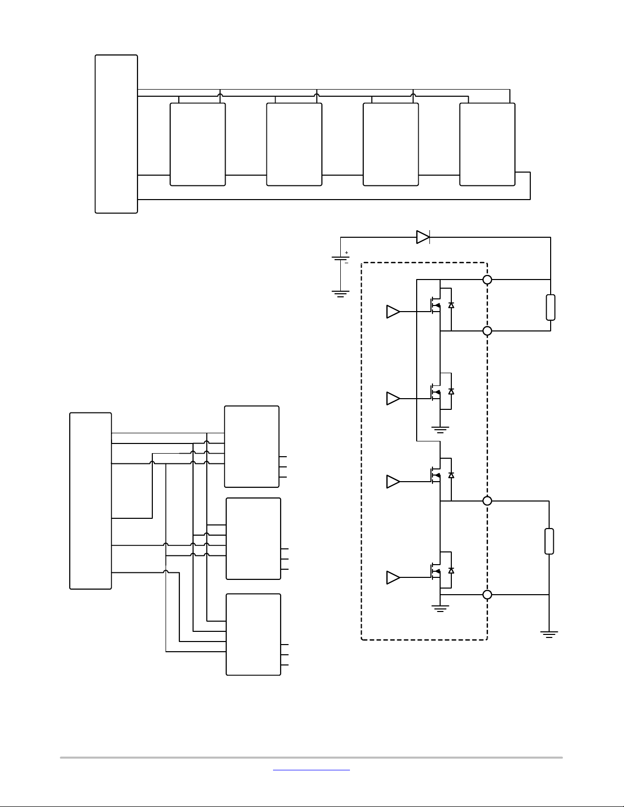
NCV7703C
CSB SCLK
NCV7703C
microprocessor
SI SO
CSB SCLK
NCV7703C
SI SO
Figure 17. Daisy Chain Operation
Parallel Control
A more efficient way to control multiple SPI compatible
devices is to connect them in a parallel fashion and allow
each device to be controlled in a multiplex mode. The
diagram below shows a typical connection between the
microprocessor or microcontroller and multiple SPI
compatible devices. In a daisy chain configuration, the
programming information for the last device in the serial
string must first pass through all the previous devices. The
parallel control setup eliminates that requirement, but at the
cost of additional control pins from the microprocessor for
each individual CSB pin for each controllable device. Serial
data is only recognized by the device that is activated
through its respective CSB pin.
CSB SCLK
NCV7708C
SI SO
CSB SCLK
NCV7708C
SI SO
V
S
OUTx
NCV7703C
SI
SCLK
SO
CSB
chip1
CSB
microprocessor
chip2
CSB
chip3
Figure 18. Parallel Control
SI
SCLK
CSB
OUT1
SO
OUT2
OUT3
NCV7703C
SI
SCLK
CSB
OUT1
SO
OUT2
OUT3
NCV7703C
SI
SCLK
CSB
OUT1
SO
OUT2
OUT3
Additional Application Setup
In addition to the cascaded H−Bridge application shown
in Figure 1, the NCV7703C can also be used as a high−side
driver or low−side driver (Figure 19).
OUTx
GND
Figure 19. High−Side / Low−Side Application Drawing
Any combination of H−bridge and high or low−side
drivers can be designed in. This allows for flexibility in
many systems.
www.onsemi.com
19
Page 20

MECHANICAL CASE OUTLINE
PACKAGE DIMENSIONS
14
1
SCALE 1:1
SOIC−14 NB
CASE 751A−03
ISSUE L
DATE 03 FEB 2016
14
H
M
0.25 B
0.10
14X
0.58
D
M
13X
e
SOLDERING FOOTPRINT*
6.50
1
A
B
8
E
71
b
S
M
0.25 B
A
C
A
A1
SEATING
C
PLANE
14X
1.18
S
1.27
PITCH
DETAIL A
h
X 45
_
M
NOTES:
1. DIMENSIONING AND TOLERANCING PER
ASME Y14.5M, 1994.
2. CONTROLLING DIMENSION: MILLIMETERS.
3. DIMENSION b DOES NOT INCLUDE DAMBAR
A3
L
DETAIL A
PROTRUSION. ALLOWABLE PROTRUSION
SHALL BE 0.13 TOTAL IN EXCESS OF AT
MAXIMUM MATERIAL CONDITION.
4. DIMENSIONS D AND E DO NOT INCLUDE
MOLD PROTRUSIONS.
5. MAXIMUM MOLD PROTRUSION 0.15 PER
SIDE.
DIM MIN MAX MIN MAX
A 1.35 1.75 0.054 0.068
A1 0.10 0.25 0.004 0.010
A3 0.19 0.25 0.008 0.010
b 0.35 0.49 0.014 0.019
D 8.55 8.75 0.337 0.344
E 3.80 4.00 0.150 0.157
e 1.27 BSC 0.050 BSC
H 5.80 6.20 0.228 0.244
h 0.25 0.50 0.010 0.019
L 0.40 1.25 0.016 0.049
M 0 7 0 7
__ __
INCHESMILLIMETERS
GENERIC
MARKING DIAGRAM*
14
XXXXXXXXXG
AWLYWW
1
XXXXX = Specific Device Code
A = Assembly Location
WL = Wafer Lot
Y = Year
WW = Work Week
G = Pb−Free Package
*This information is generic. Please refer to
device data sheet for actual part marking.
Pb−Free indicator, “G” or microdot “ G”,
may or may not be present.
DIMENSIONS: MILLIMETERS
*For additional information on our Pb−Free strategy and soldering
details, please download the ON Semiconductor Soldering and
Mounting Techniques Reference Manual, SOLDERRM/D.
STYLES ON PAGE 2
DOCUMENT NUMBER:
DESCRIPTION:
ON Semiconductor and are trademarks of Semiconductor Components Industries, LLC dba ON Semiconductor or its subsidiaries in the United States and/or other countries.
ON Semiconductor reserves the right to make changes without further notice to any products herein. ON Semiconductor makes no warranty, representation or guarantee regarding
the suitability of its products for any particular purpose, nor does ON Semiconductor assume any liability arising out of the application or use of any product or circuit, and specifically
disclaims any and all liability, including without limitation special, consequential or incidental damages. ON Semiconductor does not convey any license under its patent rights nor the
rights of others.
© Semiconductor Components Industries, LLC, 2019
98ASB42565B
SOIC−14 NB
Electronic versions are uncontrolled except when accessed directly from the Document Repository.
Printed versions are uncontrolled except when stamped “CONTROLLED COPY” in red.
PAGE 1 OF 2
www.onsemi.com
Page 21

SOIC−14
CASE 751A−03
ISSUE L
DATE 03 FEB 2016
STYLE 1:
PIN 1. COMMON CATHODE
2. ANODE/CATHODE
3. ANODE/CATHODE
4. NO CONNECTION
5. ANODE/CATHODE
6. NO CONNECTION
7. ANODE/CATHODE
8. ANODE/CATHODE
9. ANODE/CATHODE
10. NO CONNECTION
11. ANODE/CATHODE
12. ANODE/CATHODE
13. NO CONNECTION
14. COMMON ANODE
STYLE 5:
PIN 1. COMMON CATHODE
2. ANODE/CATHODE
3. ANODE/CATHODE
4. ANODE/CATHODE
5. ANODE/CATHODE
6. NO CONNECTION
7. COMMON ANODE
8. COMMON CATHODE
9. ANODE/CATHODE
10. ANODE/CATHODE
11. ANODE/CATHODE
12. ANODE/CATHODE
13. NO CONNECTION
14. COMMON ANODE
STYLE 2:
CANCELLED
STYLE 6:
PIN 1. CATHODE
2. CATHODE
3. CATHODE
4. CATHODE
5. CATHODE
6. CATHODE
7. CATHODE
8. ANODE
9. ANODE
10. ANODE
11. ANODE
12. ANODE
13. ANODE
14. ANODE
STYLE 3:
PIN 1. NO CONNECTION
2. ANODE
3. ANODE
4. NO CONNECTION
5. ANODE
6. NO CONNECTION
7. ANODE
8. ANODE
9. ANODE
10. NO CONNECTION
11. ANODE
12. ANODE
13. NO CONNECTION
14. COMMON CATHODE
STYLE 7:
PIN 1. ANODE/CATHODE
2. COMMON ANODE
3. COMMON CATHODE
4. ANODE/CATHODE
5. ANODE/CATHODE
6. ANODE/CATHODE
7. ANODE/CATHODE
8. ANODE/CATHODE
9. ANODE/CATHODE
10. ANODE/CATHODE
11. COMMON CATHODE
12. COMMON ANODE
13. ANODE/CATHODE
14. ANODE/CATHODE
STYLE 4:
PIN 1. NO CONNECTION
2. CATHODE
3. CATHODE
4. NO CONNECTION
5. CATHODE
6. NO CONNECTION
7. CATHODE
8. CATHODE
9. CATHODE
10. NO CONNECTION
11. CATHODE
12. CATHODE
13. NO CONNECTION
14. COMMON ANODE
STYLE 8:
PIN 1. COMMON CATHODE
2. ANODE/CATHODE
3. ANODE/CATHODE
4. NO CONNECTION
5. ANODE/CATHODE
6. ANODE/CATHODE
7. COMMON ANODE
8. COMMON ANODE
9. ANODE/CATHODE
10. ANODE/CATHODE
11. NO CONNECTION
12. ANODE/CATHODE
13. ANODE/CATHODE
14. COMMON CATHODE
DOCUMENT NUMBER:
DESCRIPTION:
ON Semiconductor and are trademarks of Semiconductor Components Industries, LLC dba ON Semiconductor or its subsidiaries in the United States and/or other countries.
ON Semiconductor reserves the right to make changes without further notice to any products herein. ON Semiconductor makes no warranty, representation or guarantee regarding
the suitability of its products for any particular purpose, nor does ON Semiconductor assume any liability arising out of the application or use of any product or circuit, and specifically
disclaims any and all liability, including without limitation special, consequential or incidental damages. ON Semiconductor does not convey any license under its patent rights nor the
rights of others.
© Semiconductor Components Industries, LLC, 2019
98ASB42565B
SOIC−14 NB
Electronic versions are uncontrolled except when accessed directly from the Document Repository.
Printed versions are uncontrolled except when stamped “CONTROLLED COPY” in red.
PAGE 2 OF 2
www.onsemi.com
Page 22

ON Semiconductor and are trademarks of Semiconductor Components Industries, LLC dba ON Semiconductor or its subsidiaries in the United States and/or other countries.
ON Semiconductor owns the rights to a number of patents, trademarks, copyrights, trade secrets, and other intellectual property. A listing of ON Semiconductor’s product/patent
coverage may be accessed at www.onsemi.com/site/pdf/Patent−Marking.pdf
ON Semiconductor makes no warranty, representation or guarantee regarding the suitability of its products for any particular purpose, nor does ON Semiconductor assume any liability
arising out of the application or use of any product or circuit, and specifically disclaims any and all liability, including without limitation special, consequential or incidental damages.
Buyer is responsible for its products and applications using ON Semiconductor products, including compliance with all laws, regulations and safety requirements or standards,
regardless of any support or applications information provided by ON Semiconductor. “Typical” parameters which may be provided in ON Semiconductor data sheets and/or
specifications can and do vary in different applications and actual performance may vary over time. All operating parameters, including “Typicals” must be validated for each customer
application by customer’s technical experts. ON Semiconductor does not convey any license under its patent rights nor the rights of others. ON Semiconductor products are not
designed, intended, or authorized for use as a critical component in life support systems or any FDA Class 3 medical devices or medical devices with a same or similar classification
in a foreign jurisdiction or any devices intended for implantation in the human body. Should Buyer purchase or use ON Semiconductor products for any such unintended or unauthorized
application, Buyer shall indemnify and hold ON Semiconductor and its officers, employees, subsidiaries, affiliates, and distributors harmless against all claims, costs, damages, and
expenses, and reasonable attorney fees arising out of, directly or indirectly, any claim of personal injury or death associated with such unintended or unauthorized use, even if such
claim alleges that ON Semiconductor was negligent regarding the design or manufacture of the part. ON Semiconductor is an Equal Opportunity/Affirmative Action Employer. This
literature is subject to all applicable copyright laws and is not for resale in any manner.
. ON Semiconductor reserves the right to make changes without further notice to any products herein.
PUBLICATION ORDERING INFORMATION
LITERATURE FULFILLMENT:
Email Requests to: orderlit@onsemi.com
ON Semiconductor Website: www.onsemi.com
TECHNICAL SUPPORT
North American Technical Support:
Voice Mail: 1 800−282−9855 Toll Free USA/Canada
Phone: 011 421 33 790 2910
Europe, Middle East and Africa Technical Support:
Phone: 00421 33 790 2910
For additional information, please contact your local Sales Representative
◊
www.onsemi.com
1
 Loading...