

Page 1
12 Channels 60 mA LED
Linear Current Driver I
2
C
Controllable for Automotive
Applications
NCV7685
The NCV7685 consists of twelve linear programmable constant
current sources with common reference. The part is designed for use in
the regulation and control of LED for automotive applications. The
NCV7685 allows 128 different duty cycle levels adjustable using
pulse width modulation (PWM) independently for each output
channel programmable via I
be chosen in four different configurations up to 1200 Hz. The device
can be used with micro−controller applications using the I
stand−alone applications where a choice could be done in between 2
different static configuration settings. The IC also provides 3.3 V
voltage reference to the application for loads up to 1 mA.
LED brightness level is easily programmed using an external
resistor. Each channel has an internal circuitry to detect open−load
conditions with an optional auto−recovery mode. If one driver is in
open−load condition, all other channels could be turned off according
to the programmable bit setting.
The device is available in small body size SSOP24−EP package.
Features
• 12 Common Current Programmable Sources up to 60 mA
• Independent PWM Duty Cycle Control for each Channel via PC
• Common PWM Duty Cycle Control via I
• On−Chip 150, 300, 600 and 1200 Hz PWM
• Open LED String Diagnostics
• Low Dropout Operation for Pre−Regulator Applications
• Single Resistor for Current Set Point
• Voltage Reference 3.3 V/1 mA
• 8 Bits I
2
C Interface with CRC8 Error Detection
• OTP Bank for Stand−Alone Operation (2 Configurations)
• Output Enable Pin
• Detection and Protection Against Open Load and Under−Voltage
• Over Temperature Detection and Protection
• Low Emission with Spread Spectrum Oscillator
• NCV Prefix for Automotive and Other Applications Requiring
Unique Site and Control Change Requirements; AEC−Q100
Qualified and PPAP Capable
• SSOP24−EP Packaging
2
C serial interface. PWM frequency can
2
C bus or in
2
C
www.onsemi.com
SSOP24−NB EP
CASE 940AQ
MARKING DIAGRAM
NCV7685
AWLYYWW
G
NCV7685 = Specific Device Code
A = Assembly Location
WL = Wafer Lot
YY = Year
WW = Work Week
G = Pb−Free Package
(Note: Microdot may be in either location)
ORDERING INFORMATION
Device Package Shipping†
NCV7685DQR2G SSOP24−EP
(Pb−Free)
†For information on tape and reel specifications,
including part orientation and tape sizes, please
refer to our Tape and Reel Packaging Specification
Brochure, BRD8011/D.
2500/
Tape & Reel
Applications
• Dashboard Applications
• Rear Combination Lamps (RCL)
• Daytime Running Lights (DRL)
• Fog Lights
• Center High Mounted Stop Lamps (CHMSL) Arrays
• Turn Signal and Other Externally Modulated Applications
© Semiconductor Components Industries, LLC, 2017
October, 2020 − Rev. 2
1 Publication Order Number:
NCV7685/D
Page 2
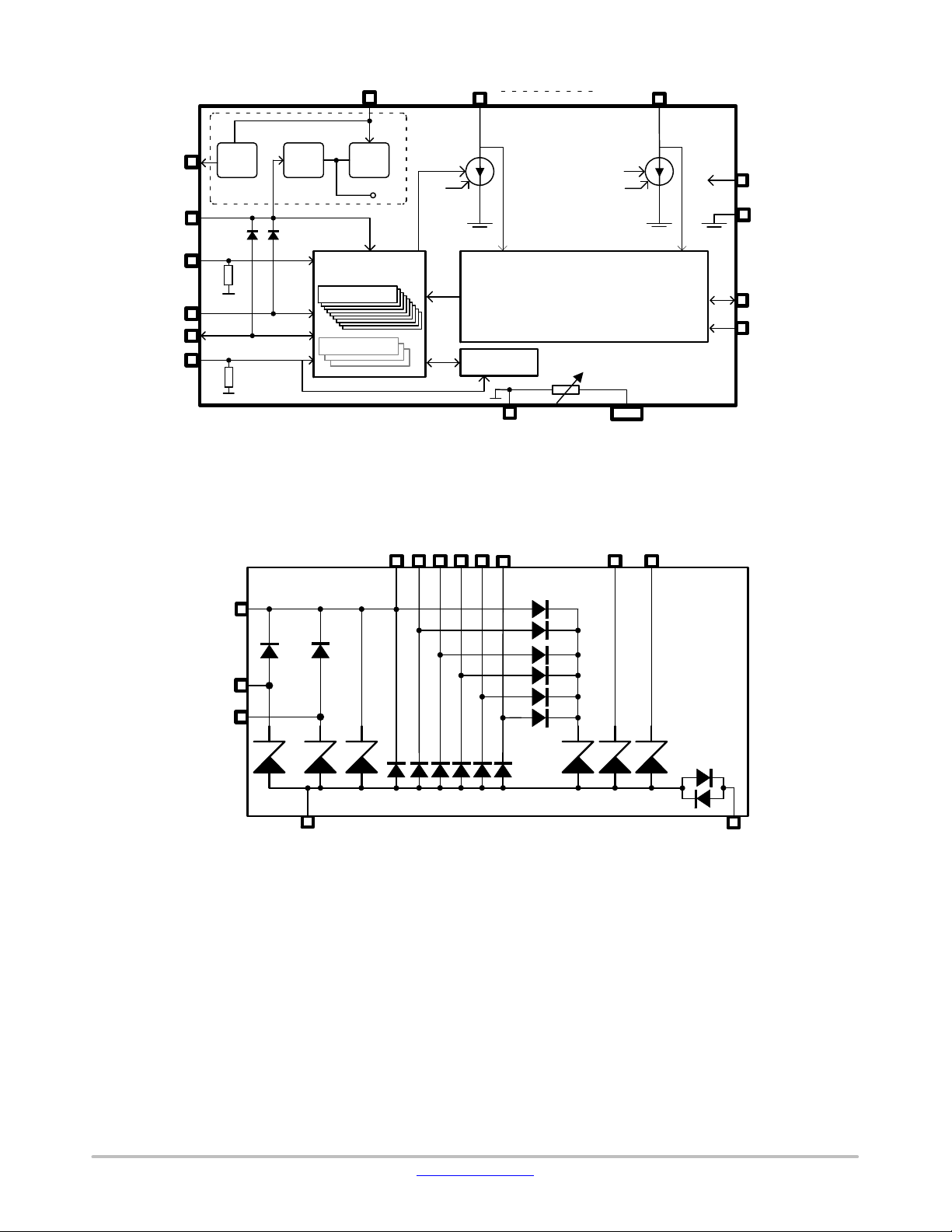
NCV7685
VCC
VDD
OEN
SCL
SDA
CONF
3V3
REG
Life Support
Vint.
REG
VS
Vint.
REG
Vint.
Registers
PWM Registers
OUT1
ctrl
Iset
60 mA
I2C
Diagnostic control
OTP
GND
Figure 1. Block Diagram
EXPOSED PAD
OUT12
ctrl
Iset
NCV7685
Iset
60mA
Iset
GNDP
DIAG
DIAGEN
VDD
SCL
SDA
GND
VS
OUTx
OEN
DIAG
DIAGEN
CONF
Figure 2. ESD Schematic
VCC
ISET
GNDP
www.onsemi.com
2
Page 3
NCV7685
Vsupply
OUT1
OUT2
OUT3
OUT4
OUT5
OUT6
OUT7
OUT8
OUT9
OUT10
OUT11
OUT12
AWLYYWW
NCV7685
G
Figure 3. Pinout Diagram
VDD
SCL
SDA
OEN
DIAG
GNDP
DIAGEN
VS
V
CC
CONF
ISET
GND
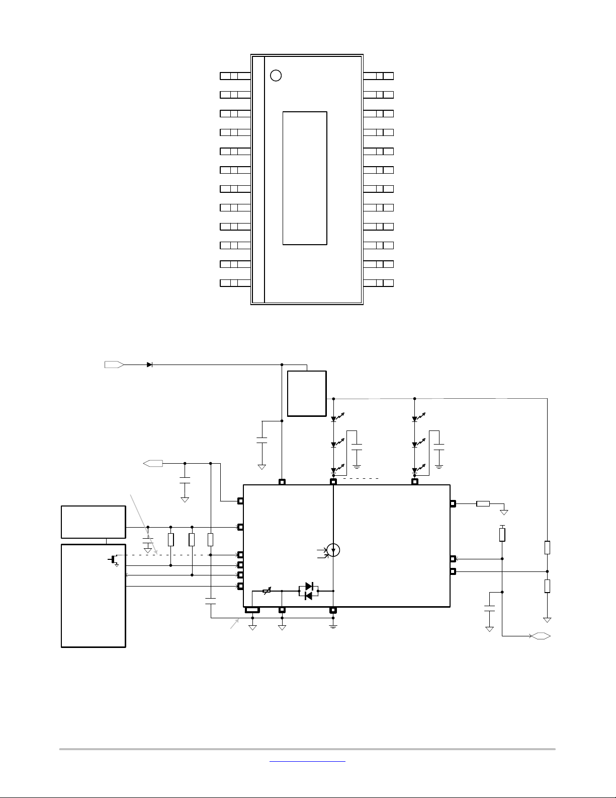
MRA4003T3G
e.g. sensor
Optional connection if MCU
control of OEN input is required.
3.3V/5V
LDO
Open Drain
GPIO structure
2
I
C {
Micro−
controller
100nF
4.7K
CVDD
R5
This GND−track is exclusively
for COEN connection. (to avoid
common impedance coupling from
other GND−currents)
Figure 4. Application Diagram with Micro−controller (I2C Mode)
R6
4.7K
C2
1nF
R7
10K
COEN
10nF
VCC
VDD
OEN
SCL
SDA
CONF
EXPOSED
100 nF
PAD
C1
VS
LDO
or
DC/DC
OUT1
GND
ctrl
Iset
60 mA
GNDP
C
OUT1
(optional)
1nF
OUT12
V
STRING
ctrl
Iset
60mA
NCV7685
C
OUT12
(optional)
1nF
Iset
Iset
DIAG
DIAGEN
(optional)
C
R1
2.2K
DIAG
1nF
R4
10K
VCC
R2
10K
R3
2.2K
www.onsemi.com
3
Page 4
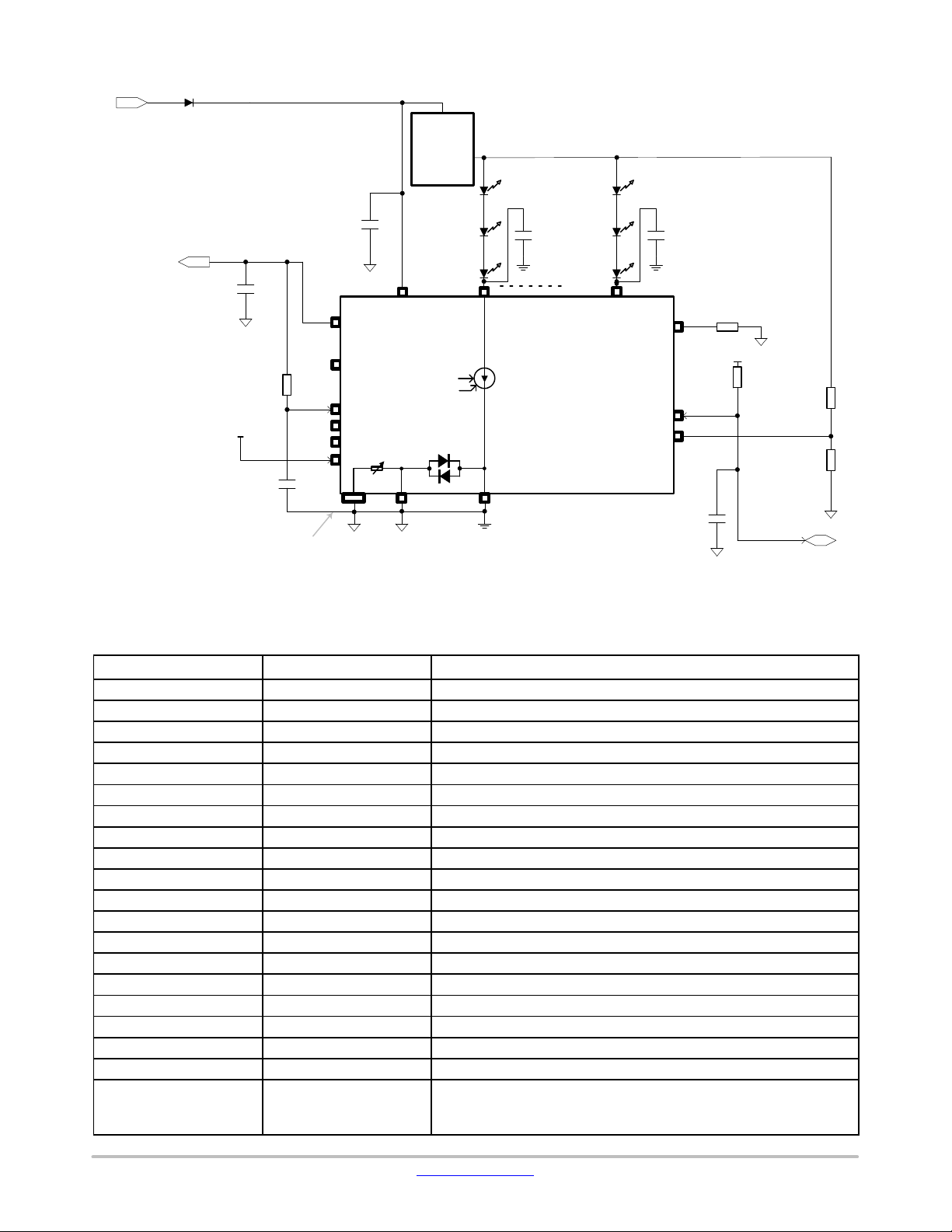
Vsupply
MRA4003T3G
NCV7685
LDO
or
DC/DC
V
STRING
C1
100nF
e.g. sensor
C2
1nF
VCC
VDD
R7
10 K
VS
C
10 nF
This GND−track is exclusively for
COEN connection. (to avoid
common impedance coupling from
other GND−currents)
Figure 5. Application Diagram without Micro−controller (Stand Alone Mode)
Table 1. PIN FUNCTION DESCRIPTION
Pin #
1 OUT1 Channel 1 Current Output to LED
2 OUT2 Channel 2 Current Output to LED
3 OUT3 Channel 3 Current Output to LED
4 OUT4 Channel 4 Current Output to LED
5 OUT5 Channel 5 Current Output to LED
6 OUT6 Channel 6 Current Output to LED
7 OUT7 Channel 7 Current Output to LED
8 OUT8 Channel 8 Current Output to LED
9 OUT9 Channel 9 Current Output to LED
10 OUT10 Channel 10 Current Output to LED
11 OUT11 Channel 11 Current Output to LED
12 OUT12 Channel 12 Current Output to LED
13 GND Signal Ground
14 ISET Current Setting/EoL Enable Pin
15 CONF Stand Alone Mode Selection Bank
16 VCC 3.3 V Voltage Reference Output (Needs External Decoupling Capacitor)
17 VS Supply Voltage Input
18 DIAGEN Diagnostic Voltage Sensing Node for V
19 GNDP Power Ground for output drivers
20 DIAG Open−drain diagnostic input/output.
OEN
OEN
SCL
SDA
CONF
EXPOSED
PAD
Label Description
VS
OUT1
ctrl
Iset
60 m A
C
OUT1
(optional)
1n F
OUT12
ctrl
Iset
60mA
C
OUT12
(optional)
1nF
Iset
Iset
DIAG
R1
2.2K
R4
10K
Vsupply
R2
10K
DIAGEN
R3
2.2K
NCV7685
GND GNDP
Reporting Open Circuit and thermal shutdown.
Normal Operation = HIGH
C
DIAG
(optional)
1 nF
Via Resistor Divider
STRING
www.onsemi.com
4
Page 5
NCV7685
Table 1. PIN FUNCTION DESCRIPTION (continued)
Pin # DescriptionLabel
21 OEN Output Enable Input
22 SDA I2C Serial Data
23 SCL I2C Serial Clock
24 VDD Digital Supply Voltage Input
epad epad True Ground
Do NOT Connect to PCB Traces other than GND
Table 2. ABSOLUTE MAXIMUM RATINGS
Symbol
V
_VS Power supply voltage:
MAX
Continuous supply voltage
Transient Voltage (t < 500 ms, “load dump”)
V
_INx Input pin voltage (DIAGEN, DIAG, CONF, OEN) −0.3 40 V
MAX
V
_OUTx Continuous Output Pin voltage
MAX
Transient Voltage (t < 500 ms, “load dump”) or during PWM
period = OFF
V
_VCC Stabilized supply voltage −0.3 3.6 V
MAX
V
_VDD Digital input supply voltage −0.3 5.5 V
MAX
V
_IO DC voltage at pins (VDD, SCL, SDA) −0.3 5.5 V
MAX
V
_ISET DC voltage at pin ISET −0.3 3.6 V
MAX
I
_GNDP Maximum Ground Current − 750 mA
MAX
T
JMAX
T
A_zap
Junction Temperature, T
OTP Zap Ambient Temperature 10 30 °C
Stresses exceeding those listed in the Maximum Ratings table may damage the device. If any of these limits are exceeded, device functionality
should not be assumed, damage may occur and reliability may be affected.
1. Integrated protection functions are designed to prevent IC destruction under fault conditions described in the datasheet. Fault conditions are
considered as outside normal operating range. Protection functions are not designed for continuous repetitive operation.
Parameter Min Max Unit
−0.3
−0.3
−0.3
−0.3
J
−40 150 °C
28
40
28
40
V
V
V
V
Table 3. ATTRIBUTES
Parameter
ESD Capability (Note 2)
ESD Voltage, HBM (Human Body Model); (100 pF, 1500 W)
− All pins
− Output pins OUTx to GND
ESD according to CDM (Charge Device Model)
− All pins
− Comer pins
ESD according to MM (Machine Mode)
− All pins
Moisture sensitivity (SSOP24−EP) (Note 3) MSL2
Storage Temperature −55 to 150 °C
Package Thermal Resistance (SSOP24−EP) (Note 4)
− Junction to Ambient, R
− Junction to Board, R
− Junction to Case (Top), R
q
JA
q
JB
q
JC
2. This device series incorporates ESD protection and is tested by the following methods:
ESD HBM tested per AEC−Q100−002 (EIA/JESD22−A114)
ESD CDM tested per EIA/JES D22/C101, Field Induced Charge Model
ESD MM according to AEC−Q100
3. For additional information, see or download ON Semiconductor’s Soldering and Mounting Techniques Reference Manual, SOLDERRM/D,
and Application Note AND8003/D.
4. Values represent thermal resistances under natural convection are obtained in a simulation on a JEDEC−standard, 2S2P; High Effective
Thermal Conductivity Test Board as specified in JESD51−7, in an environment described in JESD51−2a.
Value Unit
±2
±4
±500
±750
±150
45.8
8.8
10.1
kV
kV
V
V
V
°C/W
°C/W
°C/W
www.onsemi.com
5
Page 6
NCV7685
Table 4. ELECTRICAL CHARACTERISTICS
(5 V < VS < 18 V, 3.15 V < VDD < 5.5 V, R1 = 1.82 kΩ, −40°C ≤ T
Characteristic Symbol Test Conditions Min Typ Max Unit
GENERAL
Supply Voltage
Supply Under−Voltage VSUV VS rising 3.8 4.1 4.4 V
Supply range during
OTP zapping
Supply Under−Voltage
hysteresis
Supply Current (Vs) Is(error mode) all OUTx OFF except channel in open load
Digital supply current IDD I2C mode, VS = 12 V − 0.24 2 mA
VDD Under Voltage
detection
CURRENT SOURCE OUTPUTS
Output current
Current Matching from
channel to channel
Current Slew Rate ISRx 10% to 90% − 30 −
Open Circuit Detection
Threshold
Open load recovery in
auto−recovery mode
Product parametric performance is indicated in the Electrical Characteristics for the listed test conditions, unless otherwise noted. Product
performance may not be indicated by the Electrical Characteristics if operated under different conditions.
5. Matching formulas:
ƪ
2IOUTx(min)
IOUTx(min) ) IOUTx(max)
VS_EXT Functional extended range (limited temper-
VS_OP Parametric operation 5 − 18 V
VS_OTPzap 2.5 V ≤ ISET ≤ 3.3 V;
VSUVhys − 200 − mV
Is(active) Active Mode
VDDUV_R VDD rising − − 2.9 V
VDDUV_F VDD falling 2 − − V
IOUThot OUTx = 1 V, Tj = 150°C 50 55 60 mA
IOUTcold OUTx = 0.5 V, Tj = −40°C 50 55 60 mA
ImatchCold Tj = −40°C (Note 5) −7 0 7 %
Imatch Tj = 25°C (Note 5) −6 0 6 %
ImatchHot Tj = 150°C (Note 5) −5 0 5 %
OLDT IOUTx > 20mA 30 50 70 % of output
OLR 5 10 15 mA
* 1ƫ 100 and
ature)
VS current peak capability ≥ 70 mA
SCL = SDA = 0
Iout_VCC = 0 mA
Iout_VCC = 1 mA
VS = 16 V, Vcc unloaded
OUTx = 1 V, R1 = 2 kW
ƪ
IOUTx(min) ) IOUTx(max)
≤ 150°C, unless otherwise specified)
J
2IOUTx(max)
* 1ƫ 100
5 − 28 V
13 − 18 V
−
−
− 7 10 mA
1.2
2.2
1.5
2.5
mA
mA
mA/ms
current
Table 5. ELECTRICAL CHARACTERISTICS
(5 V < VS < 18 V, 3.15 V < V
Symbol
VOLTAGE REFERENCE
V_VCC Output Voltage Tolerance I_VCC ≤ 1 mA 3.20 3.30 3.45 V
Iout_VCC Output Current − − −1 mA
Cload_VCC Load Capacitor
INPUTS: OEN, CONF
VinL
VinH Input High Level − 1.25 1.66 V
Vin_hyst Input Hysteresis 100 250 400 mV
Rin_pd Input Pull−down Resistor 120 200 280
INPUTS: SCL, SDA
VinL Input Low Level − − 0.3×VDD V
Input Low Level 0.7 1.0 − V
< 5.5 V, R1 = 1.82 kΩ, −40°C ≤ TJ ≤ 150°C, unless otherwise specified)
DD
Parameter Test Conditions Min Typ Max Unit
ESR < 200 mW
0.9 1.0 2.5 nF
www.onsemi.com
6
kW
Page 7

NCV7685
Table 5. ELECTRICAL CHARACTERISTICS (continued)
(5 V < VS < 18 V, 3.15 V < V
Symbol UnitMaxTypMinTest ConditionsParameter
INPUTS: SCL, SDA
VinH
Vin_hyst Input Hysteresis 0.05×VDD − − V
Iout_SDA Output Current V (SDA) = 0.4 V 3 − − mA
DIAGEN PIN
VDiagenTH VS Diagnostic Enable Threshold 1.9 2.0 2.1 V
Rdiagen_pd Input Pull−down Resistor 120 200 280
DIAG PIN
VoutL Output Low Level Diagnostic Activated,
DiagRes Diagnostic Reset Voltage 1.65 1.80 1.95 V
tp_DIAG Filter Time to Set the DIAG Fail Pin in
DIAG_leak DIAG Output Leakage VDIAG = 5 V − − 10
ISET INPUT PIN
VISET Global Current Setting 0.94 1.0 1.06 V
K IOUT ISET Factor − 100 − −
tsetupISET Setup−up Time to 90% of the ISET
INTERNAL PWM CONTROL UNIT (OUT1− OUT12)
Symbol Parameter Test Conditions Min Ty p Max Unit
PWM1 PWM1 Frequency, I2C Mode Configuration Via I2C 132 150 168 Hz
PWM2 PWM2 Frequency, I2C Mode Configuration Via I2C 264 300 336 Hz
PWM3 PWM3 Frequency, I2C Mode Configuration Via I2C 528 600 672 Hz
PWM4 PWM4 Frequency, I2C Mode Configuration Via I2C 1056 1200 1344 Hz
Product parametric performance is indicated in the Electrical Characteristics for the listed test conditions, unless otherwise noted. Product
performance may not be indicated by the Electrical Characteristics if operated under different conditions.
Input High Level 0.7×VDD − − V
Failure Mode
Regulated Value
< 5.5 V, R1 = 1.82 kΩ, −40°C ≤ TJ ≤ 150°C, unless otherwise specified)
DD
Idiag = 1 mA
Idiag = 1 mA − 10 20
VS > 5 V − − 50
− 0.2 0.4 V
kW
ms
mA
ms
Table 6. THERMAL WARNING AND THERMAL SHUTDOWN PROTECTION
Symbol
Tjwar_on Thermal Warning Threshold (Junction Temperature) − TSD−30 − °C
TSD Thermal Shutdown Threshold (Junction Temperature)
Tjsd_hys Thermal Shutdown Hysteresis 10 − 15 °C
T
Increasing
J
General
The NCV7685 is a twelve channel LED driver. Each
output can drive currents up to 60 mA/channel and are
programmable via an external resistor. The target
applications for the device are in automotive rear lighting
systems and dashboard applications. The device can be used
with micro−controller applications using the I
stand−alone applications. In both cases it is mandatory to
supply the LED channels by an external ballast transistor, or
by an LDO or a DC/DC to have low voltage drop on the
outputs which will lead to a decrease in power dissipation in
the device. In order to have very low electromagnetic
emission, this device has an embedded spread spectrum
oscillator.
Parameter Min Typ Max Unit
160 − 180 °C
Output Current Programming (I
SET/IOUTx
The maximum current can be defined with the Iset input
pin. The equations below can be used to calculate this
maximum output current:
Iset + 1VńR1
2
C bus or in
IOUTx + K Iset
Example:
R1 = 2 kΩ
using eq. 1 → Iset = 500 μA
and using eq. 2 → IOUTx = 50 mA
To avoid potential disturbances when all drivers are
activated at the same time, a typical activation delay of
400 ns between groups of 2 consecutive outputs is
implemented (see Figure 6).
)
(eq. 1)
(eq. 2)
www.onsemi.com
7
Page 8

NCV7685
PWM period counter
PWM signal
driver 1
driver 2
driver 3
driver 4
driver 5
driver 6
driver 7
driver 8
driver 9
driver 10
driver 11
driver 12
Power Supply and Voltage Reference (VS, VCC, VDD)
0123456789101112131415161718192021222324252627
Figure 6.
VS is the analog power supply input of the device. VS
supply is monitored with respect to the crossing of VSUV
level (typ. 4.1 V). When VS rises above VSUV, the device
starts the power−up state. When VS is above the VS_OP
minimum level (typ. 5 V), the device can work properly.
VCC is a voltage reference providing 3.3 V derived from
the VS main supply. It is able to deliver up to 1 mA and is
primarily intended to supply 3.3 V loads. If VCC output
reference is not used, then the VCC capacitor can be omitted.
VDD is the digital power supply input of the device.
5V
VS
Activation of the VDD can be
VDD
before or after VS supply
ISET resistor is connected to the I
pin, the access to the
SET
OTP registers is not possible. Zapping is only possible with
VS above 13 V. The outputs are disabled as soon as 2.5 V is
applied to the ISET pin. After the ID_LOCK_OTP I2C
message is properly received, no further OTP zapping is
possible.
Output Enable (OEN)
When the OEN input voltage is high, all output channels
are programmed according to the I2C or SAM
configuration. When OEN voltage is below 0.7 V, all
outputs are disabled in the SAM or I2C mode regardless on
the registers setting. If the OEN pin is left floating, the
internal pull down resistor will cause switching off all
channels. The OEN pin has to have max slope of 5 mV for
first 10 ms until VCC is activated. The recommended
examples are shown in Figure 4 and Figure 5. The Figure 11
shows the example of the driving multiple NCV7685 drivers
from one MCU.
*)VCC is internally
VCC
tsetupISET is up to 50
OEN
OEN pin has to have max slope of
5 mV/10 μs until VCC is activated.
Slope on the OEN pin has to be slower
than slope on the VS or slope on VDD
(depends on what comes first)
Figure 7. Power−up Sequence for OEN pin
Ground Connections (GND: Pin 13 and GNDP Pin 19)
μs
derived from VS
The device ground connection is split to two pins called
GND and GNDP. Both pins have to be connected on the
application PCB.
Chip Select for OTP Programing (Using I
SET
)
The device can be programmed using the I2C bus in End
of Line cases. When the voltage on the ISET pin is pulled
higher than 2.5 V, the device can be set in OTP control mode
via the I2C bus. During normal mode where only an external
www.onsemi.com
Configuration (CONF)
When the CONF input voltage will be below 0.7 V the
configuration 1 will be selected (One Time Programmable
OTP 1 register called SAM_CONF_1) and when the CONF
input voltage will be above 1.66 V the configuration 2 will
be selected (OTP 2 register called SAM_CONF_2). There
is ability to change the configuration in error mode (either
with CONF in SAM or through I
I2C Bus (SCL, SDA)
2
C in I2C mode).
The I2C bus consists of two wires, Serial Data (SDA) and
Serial Clock (SCL), carrying information between the
devices connected on the bus. Each device connected to the
bus is recognized by a unique address and operates as either
a transmitter or receiver, depending on the function of the
device. The NCV7685 can both receive and transmit data
with CRC8 error detection algorithm. The NCV7685 is a
slave device.
SDA is a bi−directional line connected to a positive supply
voltage via an external pull−up resistor. When the bus is free
both lines are HIGH. The output stages of the devices
connected to the bus must have an open drain to perform the
8
Page 9

NCV7685
wired−AND function. Data on the I2C bus can be transferred
up to 400 kb/s.
Diagnostic Enabling (DIAGEN)
The device is capable to detect for each independent
channel an open load condition. Versus the number of LEDs
and the Vstring voltage supply, a wrong open load condition
can be detected if the fault detection is activated when there
is not enough voltage across the LEDs. This threshold can
be programmable thanks to an external divider connected to
the DIAGEN pin. When the divided voltage is below a
typical value of 2 V, the LED diagnostic is disabled. When
the divided voltage is above the typical value of 2 V, the LED
diagnostic is enabled.
Diagnostic Feedback (DIAG)
The DIAG is an open drain output pin who can alert a
microcontroller as soon as one of the outputs is in error mode
(DIAG Low = open load or thermal shut−down or I
shorted). Forcing the DIAG pin below 1.8 V will force a
fault condition if the DIAGEN input pin is above a typical
value of 2 V. If the DIAGEN input pin is below the typical
value of 2 V then forcing the DIAG input pin will not have
any effect.
Due to certain sensitivity on the DIAG pin during the
startup, it is recommended to have the pull−up resistor
connected to the VCC supply. In case if the application
deviate from the proposal mentioned in the Figure 4 or
Figure 5, the power−up sequence has to follow the timing
diagrams in the Figure 8 or Figure 9.
5V
VS
DIAG
VCC
*) VCC is internally
derived from VS
SET
Figure 9. Power−up Sequence for DIAG pin. VDD is
supplied first, VS comes up later or equal.
Parallel Outputs
The maximum rating per output is 60 mA. In order to
increase system level LED string current, parallel
combinations of any number of outputs is allowed.
Combining all 12 outputs will allow for a maximum system
level string current design of 720 mA.
Required Time Delay for OTP Zapping
As soon as the ID_LOCK_OTP message is received, the
2
I
C acknowledge is immediately sent out to the MCU.
However, the internal circuitries still requires 500 ms time
delay to complete the OTP zapping of one OTP bit.
Therefore, no I2C confirmation is send. The number of OTP
bits that are zapped corresponds with each change from the
default values. It is needed 16.5 ms in total to successfully
finish the zapping sequence of all 32 customer bits + one
internal bit. The verification of the OTP banks can be done
by readout of the ID_READ_OTP I
2
C message after
zapping delay.
VDD
t
setupISET
Figure 8. Power−up Sequence for DIAG pin. VS is
is up to 50 mst ≥ 0 ms
supplied first, VDD comes up later.
www.onsemi.com
9
Page 10

3.3V/5V
LDO
Open Drain
GPIO structure
I2C
Micro−
controller
V
BAT
MRA4003T3G
VCC_U1
C2
1nF
C
VDD
100nF
R5
4.7K
R6
4.7K
{
C
OEN
100nF
This GND−track is exclusively for
COEN connection. (to avoid
common impedance coupling from
other GND−currents)
Figure 10. Example of using Multiple NCV7685 Drivers Controlled from One MCU
NCV7685
V
SUPPLY
LDO
or
DC/DC
C1
100nF
R7
5K
R
59K
OEN
VCC
VDD
OEN
SCL
SDA
CONF
EP
VS
GND
V
STRING
C
OUT1
(optional)
1nF
OUT1 OUT12
NCV7685
DIAGEN
GNDP
Iset
DIAG
C
(optional)
1nF
VCC_U1
100K
C
33nF
U1
OUT12
2.2K
R4
DIAG
V
SUPPLY
C1
100nF
R1
_
R2
10K
R3
2.2K
C2
1nF
To VDD supply
R
C
VDD
100nF
OEN
59K
To MCU
C
OEN
100nF
This GND−track is exclusively
for COEN connection. (to avoid
common impedance coupling from
other GND−currents)
VCC
VDD
OEN
SCL
SDA
CONF
EP
VS
DIAG
V
STRING
C
(optional)
OUT1 OUT12
NCV7685
GND
GNDP
OUT1
1nF
ctrl
Iset
mA
DIAG
DIAGEN
(optional)
C
(optional)
1nF
U2
C
DIAG
1nF
OUT12
2.2K
R1
R2
10K
R3
2.2K
www.onsemi.com
10
Page 11

NCV7685
DIGITAL PART AND I2C REGISTERS
The I2C bus consists of two wires, serial data (SDA) and
serial clock (SCL), carrying information between the
devices connected on the bus. Each device connected to the
bus is recognized by a unique address. The NCV7685 can
both receive and transmit data with CRC8 error detection
Table 7. IDENTIFIER ADDRESSING (ID) MESSAGE
Name
ID_I2C_CONF 00 W I2C_CONF
ID_PWM 01 W PWM_DUTY
ID_PWM_CONF 02 W PWM_CONF, PWM_DUTY_EN
ID_PWM_ALL 03 W PWM_D1, PWM_D2, PWM_D3, PWM_D4, PWM_D5, PWM_D6,
ID_WRITEALL 04 W I2C_CONF, PWM_CONF, PWM_DUTY_EN
ID_STATUS 08 R I2C_STATUS
ID_FAULT 09 R FAULT_STATUS
ID_READALL 0A R I2C_CH_STATUS, I2C_STATUS, FAULT_STATUS
ID_SET_OTP 20 W SAM_CONF_1, SAM_CONF_2, ADD_SAM_SET
ID_LOCK_OTP 21 W SAM_CONF_1, SAM_CONF_2, ADD_SAM_SET
ID_READ_OTP 28 R ID_VERS_1, ID_VERS_2, SAM_CONF_1, SAM_CONF_2, ADD_SAM_SET
ID Access type Name of Register Addressed
PWM_D7, PWM_D8, PWM_D9, PWM_D10, PWM_D11, PWM_D12
algorithm. The NCV7685 is a slave device only. Generation
of the signals on the I
2
C bus is always the responsibility of
the master device.
They are multiple kinds of message structure possible
versus ID code received.
There are 3 kinds of registers, Hard Coding, OTP and
volatile registers.
Hard Coding
Registers:
ID_VERS_1
ID_VERS_2
OTP
Registers:
ADD_SAM_SET
SAM_CONF_1
Volatile
Registers:
I2C_CONF
I2C_STATUS
I2C_CH_STATUS
FAULT_STATUS
PWM_DUTY
PWM_D1 − PWM_D12
PWM_DUTY_EN
PWM_CONF
SAM_CONF_2
Format of the I2C frames
S 0 A ID A P
NCV7685 address NCV7685 address
‘0’ = Write
From master to NCV7685
From NCV7685 to master
S = Start condition
P = Stop condition
A = Acknowledge
A* = Not acknowledge
N bytes +
acknowledge
Figure 11. Format of I2C Write Access Frames
NCV7685
0 A CRC A*ID AA
NCV7685
address
Sr
NCV7685
addressaddress
1 A Data A PCRC A*S
CRC AData AA
‘0’ = Write
From master to NCV7685
From NCV7685 to master
Figure 12. Format of I2C Read Access Frames
Remark: CRC byte is not transmitted when CRC
protection is turned off (ERREN = 0)
www.onsemi.com
11
‘1’ = Read
S = Start condition
Sr = Repeated start condition
P = Stop condition
A = Acknowledge
A* = Not acknowledge
N bytes +
acknowledge
Page 12

NCV7685
P
CRC
P
P
CRC
CRC
PWM_D3
PWM_DUTY_EN[7:0]
CRC
CRC
CRC
FAULT_STATUS[7:0]
FAULT_STATUS[15:8]
I2C_STATUS
Acknowledges are ommited
S = Start condition
Sr = Repeated start condition
P = Stop condition
I2C_CH_STATUS[15:8] I2C_CH_STATUS[7:0]
P
CRC
CRC
SAM_CONF_2[7:0]SAM_CONF_2[15:8]
CRC
Acknowledges are ommited
S = Start condition
Sr = Repeated start condition
P = Stop condition
CRC
Sr P
Sr PCRC NCV7685 address 1 I2C_STATUSS NCV7685 address 0 ID_STATUS
PWM_DUTY_EN[15:8]
I2C_CONF[15:8] I2C_CONF[7:0]
NCV7685 address
NCV7685 address
S NCV7685 address 0 ID_I2C_CONF
S NCV7685 address 0 ID_PWM PWM_DUTY
S NCV7685 address 0 ID_PWM_CONF PWM_CONF PCRCNCV7685 address
PWM_D7 PWM_D8 PWM_D9 PWM_D10 PWM_D11 PWM_D12
...
NCV7685 address PWM_D4 PWM_D5 PWM_D6
S NCV7685 address 0 ID_PWM_ALL PWM_D1 PWM_D2
Sr PCRC NCV7685 address 1 FAULT_STATUS[15:8]S NCV7685 address 0 ID_FAULT FAULT_STATUS[7:0]
NCV7685 address
NCV7685 address
NCV7685 address
S NCV7685 address 0 ID_WRITEALL PWM_CONF PWM_DUTY_EN[15:8] PPWM_DUTY_EN[7:0]I2C_CONF[15:8] I2C_CONF[7:0]
CRC NCV7685 address 1
NCV7685 address
S NCV7685 address 0 ID_READALL
Figure 13. Format of I2C Frames
From master to NCV7685
From NCV7685 to master
ID_VERS_1 ID_VERS_2 SAM_CONF_1[15:8] SAM_CONF_1[7:0] ADD_SAM_SET
1
SAM_CONF_2[15:8] SAM_CONF_2[7:0] ADD_SAM_SET
SAM_CONF_1[15:8] SAM_CONF_1[7:0]
NCV7685 address
000
S NCV7685 address ID_SET_OTP
From master to NCV7685
Sr P
CRC NCV7685 address
SAM_CONF_1[15:8] SAM_CONF_1[7:0] PSAM_CONF_2[15:8] SAM_CONF_2[7:0] ADD_SAM_SET
NCV7685 address
NCV7685 address
S NCV7685 address ID_READ_OTP
S NCV7685 address ID_LOCK_OTP
From NCV7685 to master
Figure 14. Format of I2C OTP Frames
www.onsemi.com
12
Page 13

NCV7685
t
d
There is a safety mechanism implemented by repeating
the address. Since the I
2
C address is 7 bits long, first bit of
the second address byte starts with a “0” in the repeated byte
(see tables below).
Table 8.
s
1
byte
7 6 5 4 3 2 1 0
I2C device Address R/W Bit
n
2
byte
7 6 5 4 3 2 1 0
I2C device Address 0
CRC ERROR DETECTION ALGORITHM
The CRC protection is turned off by default. It can be
enabled by activation of the OTP ERREN bit (ERREN = 1).
The every I
2
C byte including both addresses with R/W flag
Example of the CRC used in the I
I2C_CONF byte = 0xCFFF and with I
(0xC0) is 0x2E.
2
C message with
2
C address 0x60
are calculated using CRC8 algorithms. The CRC
8
polynomial is following: x
+ x5 + x3 + x2 + x + 1.
HARD CODING REGISTERS
Table 9. HARD CODING REGISTERS
Bit
ID_VERS_1
Access type
Bit name ID1[7:0]
Reset value 0 1 0 0 0 0 1 1
ID_VERS_2
Access type
Bit name ID2[7:0]
Reset value 0 0 0 0 0 1 0 0
1. ID1[7:0] = 43h (ON Semiconductor device identifier)
ID2[7:0] = 04h (The actual version)
D7 D6 D5 D4 D3 D2 D1 D0
R R R R R R R R
R R R R R R R R
OTP REGISTERS
Table 10. ADD_SAM_SET
Bit
Access type R/W R/W R/W R/W R/W R/W R/W R/W
Bit name AUTOR DETONLY ERREN ADD[4:0]
Reset value 0 1 0 0 0 0 0 0
ADD[4:0] are the programmable BUS address registers
(in I2C mode ADD[6:5] = 11).
AUTOR: When AUTOR=1 (and DIAGEN is high), open
load diagnosis is performed. When a fault is detected, the
DIAG pin is set and LED driver imposes a low current on the
faulty branch alone, switching off the others. When fault is
recovered, LED driver returns to normal operation after
resetting the DIAG pin. If the DIAG pin is triggered
externally, LED driver outputs are switched off and the low
power mode is entered.
D7 D6 D5 D4 D3 D2 D1 D0
DETONLY: When DETONLY=1, open load diagnostic is
performed. When a fault is detected, the DIAG pin is set
without taking any action on the current regulation. When
fault is recovered, DIAG is reset. If the DIAG pin is
triggered externally, no action is taken.
When AUTOR = DETONLY = 0, no diagnostic performed
When AUTOR = DETONLY = 1, no change
(same as previously setting).
ERREN: When ERREN = 1, CRC error detection
2
C communication.
www.onsemi.com
algorithm is activated for I
13
Page 14

NCV7685
Table 11. SAM_CONF
Bit
SAM_CONF_1
Access type
Bit name − − − − SAM1conf[11:0]
Reset value 0 0 0 0 0 0 0 0 0 0 0 0 0 0 0 0
SAM_CONF_2
Access type
Bit name − − − − SAM2conf[11:0]
Reset value 0 0 0 0 1 1 1 1 1 1 1 1 1 1 1 1
1. SAM1conf[x] = 0 means channel is OFF and SAM1conf[x] = 1 means channel is ON
SAM2conf[x] = 0 means channel is OFF and SAM2conf[x] = 1 means channel is ON
VOLATILE REGISTERS
Table 12. I2C_CONF
Bit
Access type W W W W W W W W W W W W W W W W
Bit name I2CFLAG I2CautoR I2CdOnly PWMEN I2Cconf[11:0]
Reset value 0 0 0 0 0 0 0 0 0 0 0 0 0 0 0 0
D15 D14 D13 D12 D11 D10 D9 D8 D7 D6 D5 D4 D3 D2 D1 D0
R R R R R/W R/W R/W R/W R/W R/W R/W R/W R/W R/W R/W R/W
R R R R R/W R/W R/W R/W R/W R/W R/W R/W R/W R/W R/W R/W
D15 D14 D13 D12 D11 D10 D9 D8 D7 D6 D5 D4 D3 D2 D1 D0
I2CFLAG: the I2CFLAG should be reset whenever
standalone mode is entered. When I2CFLAG=1 and when
VDD is high, the I2C mode is activated, in all other
conditions the device is in Stand Alone Mode.
I2CautoR: When I2CautoR=1 (and DIAGEN is high),
open load diagnosis is performed. When a fault is detected,
the DIAG pin is set and LED driver imposes a low current
on the faulty branch alone, switching off the others. When
fault is recovered, LED driver returns to normal operation
after resetting the DIAG pin. If the DIAG pin is triggered
externally, LED driver outputs are switched off and the low
power mode is entered. Whenever the device is configured
in autorecovery (AUTOR in standalone mode or I2CautoR
in I2C mode), it is not allowed to put PWMDUTY = 0 or
I2CdOnly: When I2CdOnly =1, open load diagnostic is
performed. When a fault is detected, the DIAG pin is set
without taking any action on the current regulation. When
fault is recovered, DIAG is reset. If the DIAG pin is
triggered externally, no action is taken.
When I2CautoR = I2CdOnly = 0, no diagnostic
performed.
When I2CautoR = I2CdOnly = 1, no change (same as
previously setting).
PWMEN: When PWMEN = 1, PWM is activated, when
PWMEN = 0 the content of the complete register
PWM_DUTY_EN is not reset and PWM is disabled.
I2Cconf[x] = 0 means channel is OFF and I2Cconf[x] = 1
means channel is ON.
PWMDx = 0 to a channel which has detected an open load.
Table 13. I2C_STATUS
Bit
Access type R R R R R R R R
Bit name SC_Iset I2Cerr UV diagRange TW TSD DIAGERR OL
Reset value 0 0 0 0 0 0 0 0
SC_Iset: SC_Iset = 1 means there is short−circuit on the
external resistor on I
and DIAG pin is set. SC_Iset=0 no short−circuit.
I2Cerr: I2Cerr=1 means an error has been detected during
the I2C communication, I2Cerr=0 means no error during
I2C communication has been detected.
UV: the device is in under voltage condition (VS is below
VSUV threshold, all channels OFF).
D7 D6 D5 D4 D3 D2 D1 D0
diagRange: when diagRange = 1 the divided voltage is
pin and drivers are switched OFF
SET
above the typical value of 2 V (LED diagnostic is enabled),
diagRange = 0 means the divided voltage is below the
typical value of 2 V (LED diagnostic is disabled).
TW: when TW=1 the device is in the thermal warning
range (typ 140°C), this flag is just a warning no action is
foreseen on the output drivers. TW=0 means the device is
below the thermal warning range.
www.onsemi.com
14
Page 15

NCV7685
TSD: when TSD = 1 the device is in the Thermal shutdown
range, TSD = 0 means the device is below the thermal
shutdown range.
DIAGERR: DIAGERR = 1 means an error is detected by
DIAG pin forced externally.
Table 14.
SC_Iset
set when a short−circuit on the external resistor on I
Reset in case of short−circuit disappear permanently for at least 10ms.
I2Cerr
set if an error has been detected during the I2C communication.
Reset on register reading.
UV
diagRange
set when device is in under voltage condition (VS is below VSUV, all channels OFF).
set when divided voltage is above the VDiagenTH threshold.
Reset when the divided voltage is below the VDiagenTH threshold.
TW
set when junction temperature is above the Tjwar_on threshold.
Reset on register reading AND temperature is below the (Tjwar_on − Tjsd_hys) threshold
TSD
set when junction temperature is above the TSD threshold.
Reset on register reading AND temperature is below the TSD − Tjsd_hys) threshold
DIAGERR
set by DIAG pin forced low externally, latched if permanent after 10 ms.
Reset in case DIAG pin is not forced permanently for at least 10 ms.
OL
set in Open Load condition and DIAGEN is high, latched if permanent after 10 ms.
Reset if Open Load disappear permanently for at least 10 ms.
Fault information is maintained on falling DIAGEN threshold exceeded
OL: OL = 1 means at least one channel is in Open Load
condition, OL = 0 no Open Load.
pin, latched if permanent after 10 ms.
SET
Table 15. I2C_CH_STATUS
Bit D15 D14 D13 D12 D11 D10 D9 D8 D7 D6 D5 D4 D3 D2 D1 D0
Access type R R R R R R R R R R R R R R R R
Bit name I2CFLAG I2CautoR I2CdOnly PWMEN I2C_CH_STATUS[11:0]
Reset value 0 0 0 0 0 0 0 0 0 0 0 0 0 0 0 0
I2CFLAG: same as I2C_CONF register
I2CautoR: same as I2C_CONF register
I2CdOnly: same as I2C_CONF register
Remark: When NCV7685 is configured in I2C mode and
output channel OUTx is configured to operate in PWM
mode, I2C_CH_STATUS[x] shall contain value ‘1’.
PWMEN: same as I2C_CONF register
I2C_CH_STATUS[11:0]: same as I2C_CONF[11:0] bits
in I2C mode or same as SAM_CONF_1[11:0],
SAM_CONF_2[11:0] bits in Standalone mode.
Table 16. FAULT_STATUS
Bit
Access type R R R R R R R R R R R R R R R R
Bit name − − − − FAULT[11:0]
Reset value 0 0 0 0 0 0 0 0 0 0 0 0 0 0 0 0
FAULT[11:0]: when FAULT[x] = 1 the OUTx channel is
in fault mode (Open Load latched when the duration is
D15 D14 D13 D12 D11 D10 D9 D8 D7 D6 D5 D4 D3 D2 D1 D0
is working properly. The register is reset on each read
operation.
longer than 10 ms), when FAULT[x] = 0 the OUTx channel
www.onsemi.com
15
Page 16

NCV7685
Table 17. PWM_DUTY
Bit
Access type − W W W W W W W
Bit Name − PWMDUTY[6:0]
Reset Value 0 0 0 0 0 0 0 0
D7 D6 D5 D4 D3 D2 D1 D0
PWMDUTY[6:0]: logarithmic (or linear) common
dimming for all channels via embedded PWM generator
(128 steps). Following formula applies when logarithmic
dimming is selected: Duty_Cycle_Percent = 100 × α
(N−i)
where α = 0.9471 and N = 127 rounded with an accuracy
of 400 ns.
When PWMDUTY = 127 all channels ar fully switched
When PWMDUTY = 0 all channels are switched off.
Whenever the device is configured in autorecovery
(AUTOR in standalone mode or I2CautoR in I2C mode), it
is not allowed to put PWMDUTY = 0 or PWMDx = 0 to a
channel which has detected an open load.
Transmitting PWM_DUTY via I
2
C will cause setting the
value to all channels.
on.
Table 18. PWM_Dx
Bit
Access type − W W W W W W W
Bit Name − PWMDx[6:0]
Reset Value 0 0 0 0 0 0 0 0
PWMDx[6:0]: logarithmic (or linear) independent PWM
dimming for each OUTx channel via embedded PWM
generator (128 steps). Following formula applies when
logarithmic dimming is selected: Duty_Cycle_Percent =
100 × α
(N−i)
an accuracy of 400 ns.
When PWMDx = 127 the OUTx channel is fully switched
on.
When PWMDx = 0 the OUTx channel is switched off.
D7 D6 D5 D4 D3 D2 D1 D0
Whenever the device is configured in autorecovery
(AUTOR in standalone mode or I2CautoR in I2C mode), it
is not allowed to put PWMDUTY = 0 or PWMDx = 0 to a
channel which has detected an open load.
where α = 0.9471 and N = 127 rounded with
To set independent PWM Duty Cycle value to each
channel simultaneously, all twelve PWM_Dx bytes has to be
transferred via I
2
C bus in ID_PWM_ALL message. If
PWM_DUTY register is updated, all PWM_Dx bytes will
be overwritten by the same value from PWM_DUTY
register.
Table 19. PWM_DUTY_EN
Bit
Access type − − − − W W W W W W W W W W W W
Bit name − − − − PWMDUTYen[11:0]
Reset value 0 0 0 0 0 0 0 0 0 0 0 0 0 0 0 0
PWMDUTYen[11 :0] : when PWMDUTYen[x] = 1,
PWM dimming is enabled for OUTx channel, when
PWMGAINen[x] = 0 means PWM dimming is disabled for
Table 20. PWM_CONF
Bit
Access type W W W W W W W W
Bit Name − − − − − PWMLIN PWMF2 PWMF1
Reset Value 0 0 0 0 0 0 0 0
PWMLIN bit shall select between between logarithmic
(PWMLIN=0) and linear (PWMLIN=1) translation of
D15 D14 D13 D12 D11 D10 D9 D8 D7 D6 D5 D4 D3 D2 D1 D0
OUTx channel. When the PWM dimming is disabled, the
output channel is programmed according to the I2Cconf[x]
settings.
D7 D6 D5 D4 D3 D2 D1 D0
PWMF2 and PWMF1 bits set typical PWM frequency
settings according to the Table 21.
PWMDUTY bits to duty cycle of internal PWM signal.
www.onsemi.com
16
Page 17

Table 21. TYPICAL PWM FREQUENCY SETTINGS
PWMF2
0 0 150
0 1 300
1 0 600
1 1 1200
NCV7685
PWMF1 typ. PWM frequency [Hz]
Figure 15. Output Duty Cycle vs. Register Setting Figure 16. Output Duty Cycle vs. Register Setting
− Detail
ON Semiconductor is licensed by Philips Corporation to carry the I2C Bus Protocol.
www.onsemi.com
17
Page 18

MECHANICAL CASE OUTLINE
PACKAGE DIMENSIONS
SCALE 1:1
2X
NOTE 4
D
A
B
TOP VIEW
SIDE VIEW
NOTE 8
D2
BOTTOM VIEW
3.00
13
24X
A1
EE1
2X 12 TIPS
b
M
0.12 DC
A2
C
E2
NOTE 8
2X
0.20 C
24X
NOTE 5
PIN 1
REFERENCE
0.10 C
0.10
C
0.15 DC
NOTE 6
24
112
e
NOTE 6
A
M
A-B
RECOMMENDED
SOLDERING FOOTPRINT*
SSOP−24 NB EP
CASE 940AQ
A-B0.20
C
D
H
A1
0.20 C
A-B
h
SEATING
PLANE
M
0.15 DC
ISSUE O
L1
L
DETAIL A
NOTE 7
c
END VIEW
A-B
NOTES:
1. DIMENSIONING AND TOLERANCING PER ASME
Y14.5M, 1994.
2. CONTROLLING DIMENSION: MILLIMETERS.
3. DIMENSION b DOES NOT INCLUDE DAMBAR
PROTRUSION. DAMBAR PROTRUSION SHALL
BE 0.10 MAX. AT MMC. DAMBAR CANNOT BE
L2
GAUGE
PLANE
SEATING
C
PLANE
DETAIL A
h
LOCATED ON THE LOWER RADIUS OF THE
FOOT. DIMENSION b APPLIES TO THE FLAT
SECTION OF THE LEAD BETWEEN 0.10 TO 0.25
FROM THE LEAD TIP.
4. DIMENSION D DOES NOT INCLUDE MOLD
FLASH, PROTRUSIONS OR GATE BURRS. MOLD
FLASH, PROTRUSIONS OR GATE BURRS SHALL
NOT EXCEED 0.15 PER SIDE. DIMENSION D IS
DETERMINED AT DATUM PLANE H.
5. DIMENSION E1 DOES NOT INCLUDE INTERLEAD
FLASH OR PROTRUSION. INTERLEAD FLASH
OR PROTRUSION SHALL NOT EXCEED 0.25 PER
SIDE. DIMENSION E1 IS DETERMINED AT DATUM PLANE H.
6. DATUMS A AND B ARE DETERMINED AT DATUM
PLANE H.
7. A1 IS DEFINED AS THE VERTICAL DISTANCE
FROM THE SEATING PLANE TO THE LOWEST
POINT ON THE PACKAGE BODY.
8. CONTOURS OF THE THERMAL PAD ARE UNCONTROLLED WITHIN THE REGION DEFINED
BY DIMENSIONS D2 AND E2.
M
MILLIMETERS
DIM MIN MAX
---
A 1.75
A1 0.00 0.10
A2 1.651.10
b 0.19 0.30
c 0.09 0.20
D 8.64 BSC
D2 2.50 2.70
E 6.00 BSC
E1 3.90 BSC
E2 1.80 2.00
e 0.65 BSC
h 0.25 0.50
L 0.40 0.85
L1 1.00 REF
L2 0.25 BSC
M 0 8
__
GENERIC
MARKING DIAGRAM*
XXXXXXXXXG
AWLYYWW
DATE 18 AUG 2017
24X
1.15
2.20
6.40
XXXX = Specific Device Code
A = Assembly Location
WL = Wafer Lot
YY = Year
WW = Work Week
1
24X
0.40
0.65
PITCH
DIMENSIONS: MILLIMETERS
*For additional information on our Pb−Free strategy and soldering
G = Pb−Free Package
*This information is generic. Please refer to
device data sheet for actual part marking.
Pb−Free indicator, “G” or microdot “ G”,
may or may not be present. Some products
may not follow the Generic Marking.
details, please download the ON Semiconductor Soldering and
Mounting Techniques Reference Manual, SOLDERRM/D.
DOCUMENT NUMBER:
DESCRIPTION:
ON Semiconductor and are trademarks of Semiconductor Components Industries, LLC dba ON Semiconductor or its subsidiaries in the United States and/or other countries.
ON Semiconductor reserves the right to make changes without further notice to any products herein. ON Semiconductor makes no warranty, representation or guarantee regarding
the suitability of its products for any particular purpose, nor does ON Semiconductor assume any liability arising out of the application or use of any product or circuit, and specifically
disclaims any and all liability, including without limitation special, consequential or incidental damages. ON Semiconductor does not convey any license under its patent rights nor the
rights of others.
© Semiconductor Components Industries, LLC, 2019
98AON73645G
SSOP−24 NB EP
Electronic versions are uncontrolled except when accessed directly from the Document Repository.
Printed versions are uncontrolled except when stamped “CONTROLLED COPY” in red.
PAGE 1 OF 1
www.onsemi.com
Page 19

ON Semiconductor and are trademarks of Semiconductor Components Industries, LLC dba ON Semiconductor or its subsidiaries in the United States and/or other countries.
ON Semiconductor owns the rights to a number of patents, trademarks, copyrights, trade secrets, and other intellectual property. A listing of ON Semiconductor’s product/patent
coverage may be accessed at www.onsemi.com/site/pdf/Patent−Marking.pdf
ON Semiconductor makes no warranty, representation or guarantee regarding the suitability of its products for any particular purpose, nor does ON Semiconductor assume any liability
arising out of the application or use of any product or circuit, and specifically disclaims any and all liability, including without limitation special, consequential or incidental damages.
Buyer is responsible for its products and applications using ON Semiconductor products, including compliance with all laws, regulations and safety requirements or standards,
regardless of any support or applications information provided by ON Semiconductor. “Typical” parameters which may be provided in ON Semiconductor data sheets and/or
specifications can and do vary in different applications and actual performance may vary over time. All operating parameters, including “Typicals” must be validated for each customer
application by customer’s technical experts. ON Semiconductor does not convey any license under its patent rights nor the rights of others. ON Semiconductor products are not
designed, intended, or authorized for use as a critical component in life support systems or any FDA Class 3 medical devices or medical devices with a same or similar classification
in a foreign jurisdiction or any devices intended for implantation in the human body. Should Buyer purchase or use ON Semiconductor products for any such unintended or unauthorized
application, Buyer shall indemnify and hold ON Semiconductor and its officers, employees, subsidiaries, affiliates, and distributors harmless against all claims, costs, damages, and
expenses, and reasonable attorney fees arising out of, directly or indirectly, any claim of personal injury or death associated with such unintended or unauthorized use, even if such
claim alleges that ON Semiconductor was negligent regarding the design or manufacture of the part. ON Semiconductor is an Equal Opportunity/Affirmative Action Employer. This
literature is subject to all applicable copyright laws and is not for resale in any manner.
. ON Semiconductor reserves the right to make changes without further notice to any products herein.
PUBLICATION ORDERING INFORMATION
LITERATURE FULFILLMENT:
Email Requests to: orderlit@onsemi.com
ON Semiconductor Website: www.onsemi.com
TECHNICAL SUPPORT
North American Technical Support:
Voice Mail: 1 800−282−9855 Toll Free USA/Canada
Phone: 011 421 33 790 2910
Europe, Middle East and Africa Technical Support:
Phone: 00421 33 790 2910
For additional information, please contact your local Sales Representative
◊
www.onsemi.com
1
 Loading...