

Page 1
NCV7683
s
Enhanced 100 mA Linear
Current Regulator and
Controller for Automotive
Sequenced LED Lighting
The NCV7683 consists of eight linear programmable constant
current sources. The part is designed for use in the regulation and
control of LED based Rear Combination Lamps and blinking
functions for automotive applications. System design with the
NCV7683 allows for two programmed levels for stop (100% Duty
Cycle) and tail illumination (programmable Duty Cycle), or an
optional external PWM control can be implemented.
LED brightness levels are easily programmed (stop is programmed
to the absolute current value, tail is programmed to the duty cycle)
with two external resistors. The use of an optional external ballast FET
allows for power distribution on designs requiring high currents. Set
back power limit reduces the drive current during overvoltage
conditions. This is most useful for low power applications when no
external FET is used.
Sequencing functionality is activated, controlled, and programmed
by individual pins. In addition to programming of the sequence
interval, the device can sequence 8 individual output channels, 4 pairs
of output channels, 2 quad output channels, or all 8 at once (for multi
IC use at high currents).
Enhanced features of this device are a global enable function and
display sequencing.
The device is available in a SSOP−24 package with exposed pad.
Features
• Constant Current Outputs for LED String Drive
• LED Drive Current up to 100 mA per Channel
• Open LED String Diagnostic with Open−Drain Output in All Modes
• Slew Rate Control Eliminates EMI Concerns
• Low Dropout Operation for Pre−Regulator Applications
• External Modulation Capable
• On−chip 800 Hz T ail PWM Dimming
• Single Resistor for Stop Current Set Point
• Single Resistor for Tail Dimming Set Point
• Overvoltage Set Back Power Limitation
• Improved EMC Performance
• Programmable Latch−Off function on Open String
♦ Restart Option of Unaffected Strings
• Over Temperature Fault Reporting
• Global Enable
• Display Sequencing
• SSOP−24 Fused Lead Package with Exposed Pad
• AEC−Q100 Qualified and PPAP Capable
• These are Pb−Free Devices
Applications
• Rear Combination Lamps (RCL)
• Daytime Running Lights (DRL)
• Fog Lights
• Center High Mounted Stop Lamps (CHMSL) Arrays
• Turn Signal and Other Externally Modulated Applications
• Signature Lamp
www.onsemi.com
MARKING DIAGRAM
NCV7683G
SSOP24 NB EP
CASE 940AP
NCV7683 = Specific Device Code
A = Assembly Location
WL = Wafer Lot
YY = Year
WW = Work Week
G = Pb−Free Package
(Note: Microdot may be in either location)
ORDERING INFORMATION
Device Package Shipping
NCV7683DQR2G SSOP24−EP
(Pb−Free)
†For information on tape and reel specifications,
including part orientation and tape sizes, please
refer to our Tape and Reel Packaging Specification
Brochure, BRD801 1/D.
AWLYYWW
2500 /
Tape & Reel
†
© Semiconductor Components Industries, LLC, 2016
February, 2018 − Rev. 3
1 Publication Order Number:
NCV7683/D
Page 2
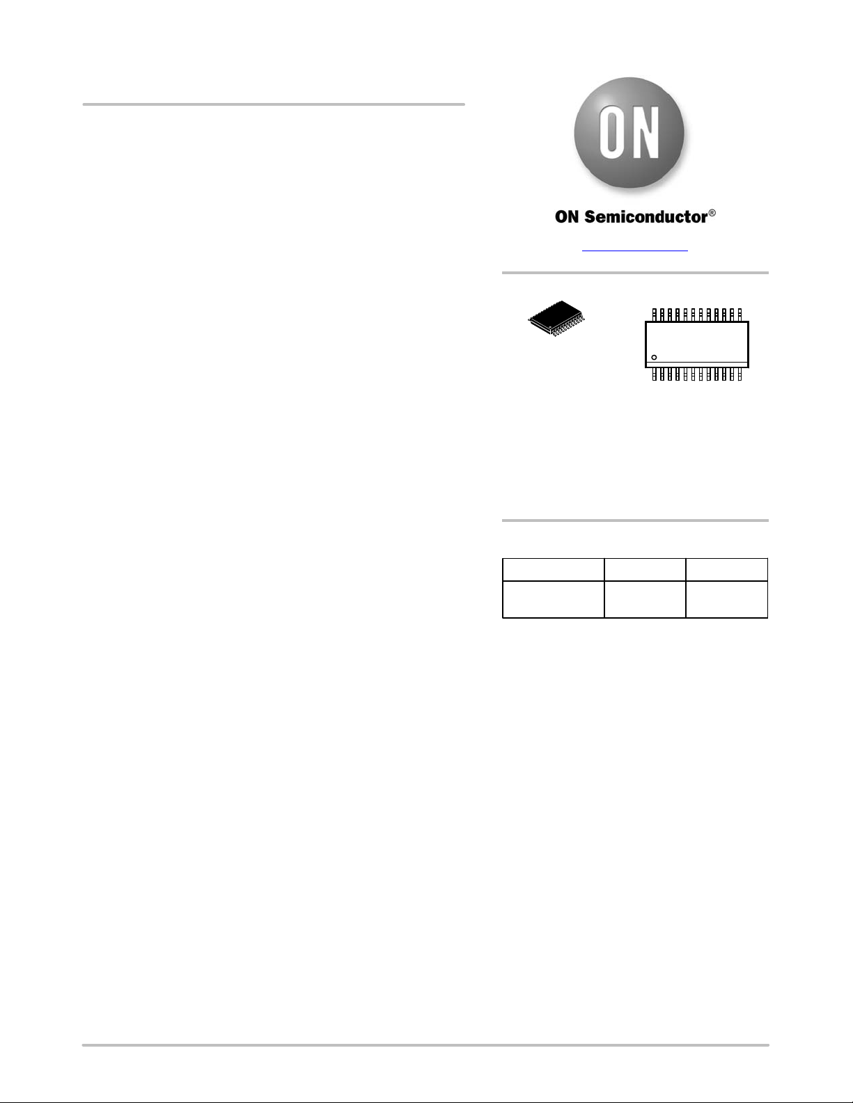
ENABLE
200k
Output
Drive Control
NCV7683
VP
Timer Circuit
Timer
Programming Current
Vref
SEQTIME
SEQ1
SEQ2
SEQON
SEQOUT
VP
Ballast
Drive
FB
STOP
DIAG
200k
DIAG
Interface
EMC Filter
200K
200K
1.8V
UVLO
−
+
FET Drive
1V
CC
−
+
Open
Circuit
Restart
SEQOUT
Open Load
Detection
Vreg
Over temperature &
Over voltage sense
Control Logic
I
RSTOP
V−I Converter
Pin
Current
Limit
8
Channel Control
Overvoltage
Soft Start,
Bias and
Reference
DIAG
Inverface
x 150
1
234567
CC
Channel
Control
Setback
Current
−20%
Output
Latch−Off
Oscillator
and PWM
2.2V
0.4V
50% IOUT
Open Load
Detect
Vreg
Irstop
−
+
Rtail
1 of 8
Output
Current
Drive
LO
Out1
Out2
Out3
Out4
Out5
Out6
Out7
Out8
GND_Signal
GND_DRV
LO
RSTOP
Figure 1. Block Diagram
Figure 2. Pinout Diagram
www.onsemi.com
2
RTAIL
ENABLE
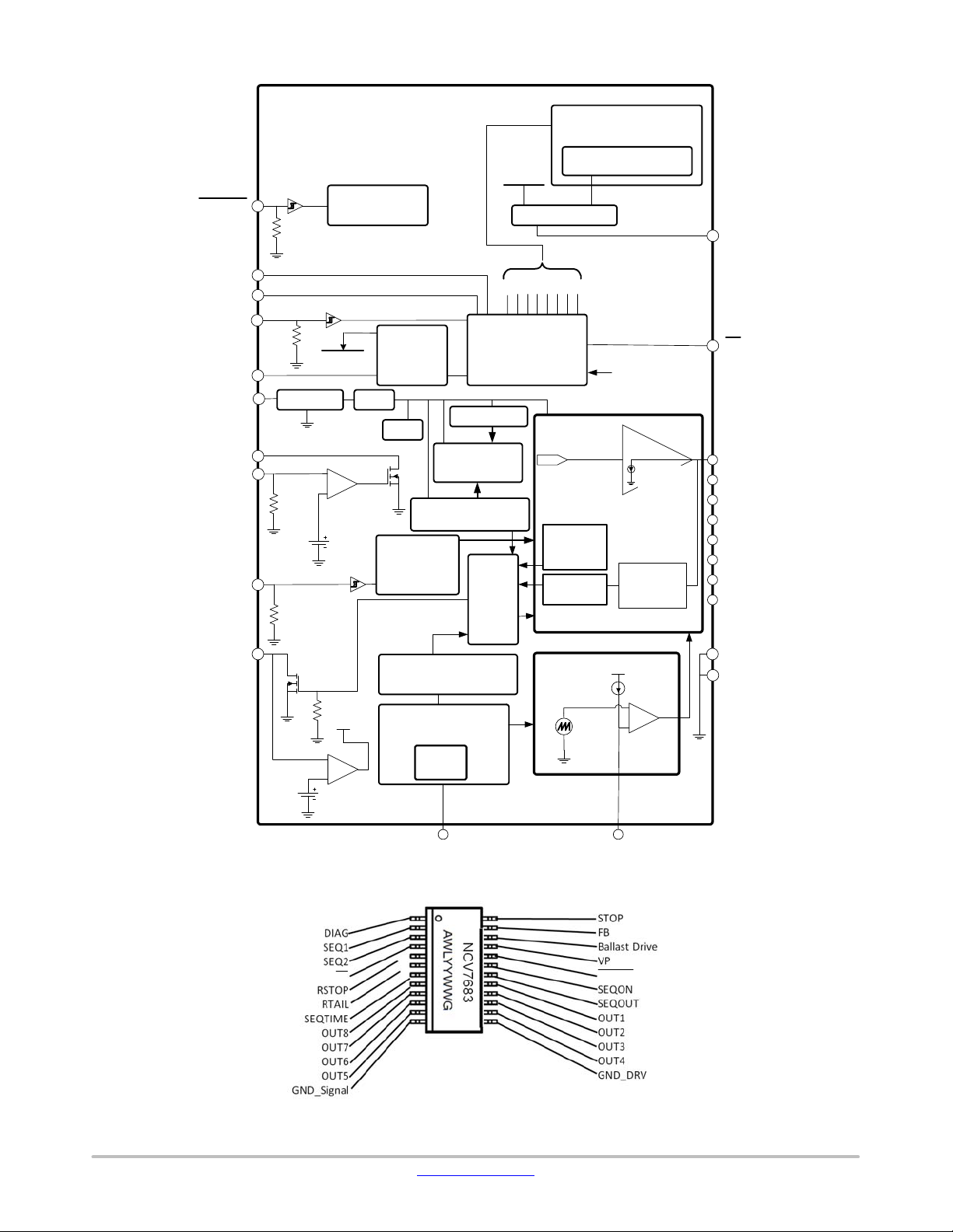
Page 3
NCV7683
TAIL
STOP
MRA4003T3G
MRA4003T3G
R1
10K
C4
10nF
C1
0.68uF
R4, 3.01K
R5, 1.62K
R2
R3
1K
NTD2955
VP
Ballast
Drive
FB
STOP
DIAG
RSTOP
RTAIL
GND_Signal
GND_DRV
ENABLE
SEQOUT
SEQ1
SEQ2
SEQON
SEQTIME
LO
NCV7683
C2
0.22uF
OUT1
OUT2
OUT3
OUT4
OUT5
OUT6
OUT7
OUT8
C3
100nF
V
STRING
Figure 3. Application Diagram with External FET Ballast Transistor
R6
9.53K
R7
1K
R6 and R7 values shown yield 10.5 V regulation on V
STRING
.
C1 is for line noise and stability considerations.
C3 is for EMC considerations.
Unused OUTx channels should be shorted to ground as OUT7 shows in this example.
MRA4003T3G
TAIL
MRA4003T3G
STOP
R1
10K
C4
10nF
0.68uF
R4, 3.01K
R5, 1.62K
C1
VP
Ballast
Drive
FB
STOP
DIAG
RSTOP
RTAIL
GND_Signal
ENABLE
SEQOUT
SEQ1
SEQ2
SEQON
SEQTIME
LO
R2
NCV7683
100nF
OUT1
OUT2
OUT3
OUT4
OUT5
OUT6
OUT7
OUT8
GND_DRV
C3
V
STRING
Figure 4. Application Diagram without the FET Ballast Transistor
When using the NCV7683 without the FET ballast transistor, tie the FB pin and Ballast Drive pin to GND.
www.onsemi.com
3
Page 4
NCV7683
Table 1. APPLICATION I/O TRUTH TABLE
STOP
EN SEQON
INPUT
1 X X X no OFF − 1
0 0 0 0 no OFF − 1
0 0 1 X no I
0 0 1 X no I
0 0 1 X yes OFF OPEN CIRCUIT*** 1
0 0 0 1 no PWM NORMAL 0
0 0 0 1 no PWM OPEN CIRCUIT*** PWM
0 1 X X no I
0 1 X X no I
0 1 X X yes OFF OPEN CIRCUIT*** 1
Reference Figures below.
X = don’t care
0 = LOW
1 = HIGH
* Open Circuit, RSTOP Current Limit, Set Back Current Limit down 20%, and thermal shutdown
**Pull−up resistor to DIAG and SEQOUT required.
*** OPEN CIRCUIT = Any string or SEQOUT open.
TAIL
MODE
OUTx LATCH OFF
= GND)
(w/ LO
OUTX
CURRENT
STOP
STOP
STOP
STOP
FAULT
STATE*
NORMAL 0
OPEN CIRCUIT*** 1
NORMAL 0
OPEN CIRCUIT*** 1
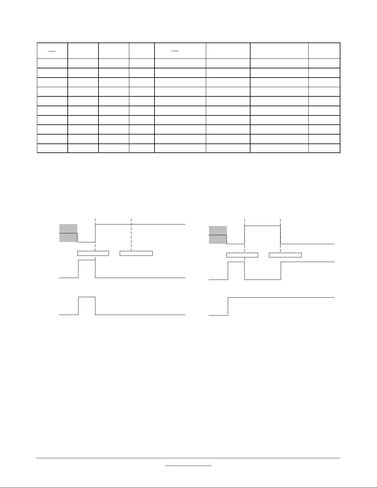
DIAG
STATE**
DIAG
Open String Occurs
on
OUTx
Current
off
on
OUTx
Current
off
Outputs with no open string.
Figure 5. DIAG timing diagram WITH
Open String Latch Active
All outputs latch off.
Open String Removed
on
Current
off
on
Current
off
DIAG
Open String Occurs
OUTx
OUTx
Outputs with no open string.
Open String Removed
Figure 6. DIAG timing diagram WITHOUT
Open String Latch Active
No outputs are turned off.
DIAG will report the state.
www.onsemi.com
4
Page 5
NCV7683
Sequencing_on
Sequencing_on
Sequence Programming Timing Diagrams
The four timing diagrams show the options available for sequencing of the 8 outputs dependent on the state of SEQ1 and SEQ2.
1. 8 individual sequence intervals.
2. 4 pairs of sequence intervals.
3. 2 quads of sequence intervals.
4. 1 single sequence interval.
ENABLE
OUT1
(current)
OUT2
(current)
OUT3
(current)
OUT4
(current)
OUT5
(current)
OUT6
(current)
OUT7
(current)
OUT8
(current)
SEQOUT
Figure 7. Sequencing Timing Diagram
Sequencing_on
ENABLE
OUT1
(current)
OUT2
(current)
OUT3
(current)
OUT4
(current)
OUT5
(current)
OUT6
(current)
OUT7
(current)
OUT8
(current)
SEQOUT
Figure 9. Sequencing Timing Diagram
Sequence
Interval
Sequence
Sequence Time
(SEQ1 = 0, SEQ2 = 0)
Interval
Sequence Time
(SEQ1 = 0, SEQ2 = 1)
ENABLE
OUT1
(current)
OUT2
(current)
OUT3
(current)
OUT4
(current)
OUT5
(current)
OUT6
(current)
OUT7
(current)
OUT8
(current)
SEQOUT
Sequencing_on
ENABLE
OUT1
(current)
OUT2
(current)
OUT3
(current)
OUT4
(current)
OUT5
(current)
OUT6
(current)
OUT7
(current)
OUT8
(current)
SEQOUT
Sequence
Interval
Sequence Time
Figure 8. Sequencing Timing Diagram
(SEQ1 = 1, SEQ2 = 0)
Sequence Time
Figure 10. Sequencing Timing Diagram
(SEQ1 = 1, SEQ2 = 1)
The sequencing function is triggered by a logic level high to low signal on the ENABLE pin.
0=ground
1=floating
www.onsemi.com
5
Page 6

NCV7683
Table 2. PIN FUNCTION DESCRIPTION
SSOP−24 Exposed
Pad Package
Pin # Label Description
1 DIAG Open−drain diagnostic output. Requires a pull−up resistor.
2 SEQ1 Grounding this pin changes the output sequencing.
3 SEQ2 Grounding this pin changes the output sequencing.
4 LO Latch Off. Ground this pin for latch off function.
5 RSTOP Stop current bias program resistor.
6 RTAIL Tail current duty cycle PWM program resistor.
7 SEQTIME Sequence Time program resistor.
8 OUT8 Channel 8 constant current output to LED.
9 OUT7 Channel 7 constant current output to LED.
10 OUT6 Channel 6 constant current output to LED.
11 OUT5 Channel 5 constant current output to LED.
12 GND_Signal Low Current Logic Ground.
13 GND_DRV High Current Driver Ground. Pin is fused to the epad.
14 OUT4 Channel 4 constant current output to LED.
15 OUT3 Channel 3 constant current output to LED.
16 OUT2 Channel 2 constant current output to LED.
17 OUT1 Channel 1 constant current output to LED.
18 SEQOUT Open−drain output. Requires a pull−up resistor. Follows ENABLE pin after delay of OUT8
19 SEQON High turns on 1−8 output sequencing.
20 ENABLE Global enable input. Low turns device on.
21 VP Supply voltage input.
22 Ballast Drive Gate drive for external power distribution PFET.
23 FB Feedback Sense node for VP regulation.
24 STOP Stop Logic Input. External Modulation Input when VP is high.
epad epad Ground. Do not connect to pcb traces other than GND.
Reporting Open Circuit, RSTOP Current Limit,
Set Back Current Limit down 20%, and thermal shutdown.
Normal Operation = LOW.
Open Load reset input.
Ground if not used (only if latchoff is not used).
Reference the sequencing section of the datasheet.
Reference the sequencing section of the datasheet.
Referenced to ground (pin 12).
Referenced to ground (pin 12).
Ground pin if using external modulation.
Referenced to ground (pin 12).
Unused pin should be grounded (pin 13).
Unused pin should be grounded (pin 13).
Unused pin should be grounded (pin 13).
Unused pin should be grounded (pin 13).
Unused pin should be grounded (pin 13).
Unused pin should be grounded (pin 13).
Unused pin should be grounded (pin 13).
Unused pin should be grounded (pin 13).
with SEQON high.
Ground if not used.
Use feedback resistor divider or connect to GND.
www.onsemi.com
6
Page 7

NCV7683
Table 3. MAXIMUM RATINGS (Voltages are with respect to device substrate.)
Rating
Supply Input (VP, Ballast Drive, STOP, DIAG, ENABLE, SEQON, SEQOUT)
DC
Peak Transient
Output Pin Voltage (OUTX) −0.3 to 40 V
Output Pin Current (OUTX) 200 mA
DIAG Pin Current 10 mA
Input Voltage (RTAIL, RSTOP, FB, SEQTIME, SEQ1, SEQ2, LO) −0.3 to 3.6 V
Junction Temperature, T
J
Peak Reflow Soldering Temperature: Lead−free
60 to 150 seconds at 217°C (Note 1)
Stresses exceeding those listed in the Maximum Ratings table may damage the device. If any of these limits are exceeded, device functionality
should not be assumed, damage may occur and reliability may be affected.
Table 4. ATTRIBUTES
Characteristic Value
ESD Capability
Human Body Model
Machine Model
Moisture Sensitivity (Note 1) MSL3
Storage Temperature
Package Thermal Resistance (Note 2)
SSOP24
Junction–to–Board, R
Junction–to–Ambient, R
Junction–to–Lead, R
1. For additional information, see or download ON Semiconductor’s Soldering and Mounting Techniques Reference Manual, SOLDERRM/D,
and Application Note AND8003/D.
2. Values represent typical still air steady−state thermal performance on 1 oz. copper FR4 PCB with 645 mm
q
JB
q
JA
q
JL
Value Unit
−0.3 to 40
40
−40 to 150 °C
260 peak °C
≥ ± 4.0 kV
≥ ± 200 V
−55 to 150°C
18°C/W
78°C/W
54°C/W
2
copper area.
V
www.onsemi.com
7
Page 8

NCV7683
Table 5. ELECTRICAL CHARACTERISTICS
(4.5 V < VP < 16 V, STOP = VP, RSTOP = 3.01 kW, RTAIL = 1.62 kW, RSEQTIME = 4.99 kW, −40°C ≤ TJ ≤ 150°C, unless otherwise specified.)
Characteristic Conditions Min Typ Max Unit
GENERAL PARAMETERS
Quiescent Current (IOUTx = 50 mA)
STOP mode
Tail mode
Fault mode
Driver Ground Pin Current (pin12) IOUT1 to IOUT8 = 50 mA − 400 500 mA
Output Under Voltage Lockout VP Rising 3.8 4.1 4.4 V
Output Under Voltage Lockout
Hysteresis
Open Load Disable Threshold 7.2 7.7 8.2 V
Open Load Disable Hysteresis − 200 − mV
THERMAL LIMIT
Thermal Shutdown
Thermal Hysteresis (Note 3) − 15 − °C
CURRENT SOURCE OUTPUTS
Output Current
Maximum Regulated Output Current 0.5V to 16V 100 − − mA
Current Matching
Line Regulation 9 V ≤ VP ≤ 16 V – 1.2 6.0 mA
Open Circuit Detection Threshold 25 mA
Current Slew Rate Iout = 44 mA, 10% to 90% points − 6 15
Overvoltage Set Back Threshold @ 99% Iout 16.0 17.2 18.4 V
Overvoltage Set Back Current VP = 20 V (Note 4) − 78 − %Iout
Diag Reporting of Set Back Current − 80 − %Iout
Output Off Leakage EN = high − − 1
FET DRIVER
Ballast Drive
DC Bias
Sink Current
Ballast Drive Reference Voltage 0.92 1.00 1.08 V
STOP / ENABLE / SEQON LOGIC
Input High Threshold
Input Low Threshold 0.70 1.00 1.44 V
VIN Hysteresis 100 250 400 mV
Input Impedance Vin = 14 V 120 200 300
3. Designed to meet these characteristics over the stated voltage and temperature recommended operating ranges, though may not be 100%
parametrically tested in production.
4. The output current degrades at a rate of 8%/V.
VP = 16 V
VP = 16 V
VP = 16 V, STOP = 0 V, OUTx = 0 mA,
Disconnected output
(Note 3) 150 175 − °C
OUTX = 0.5 V
OUTX = 1 V, R
ƪ
IOUTx(min) ) IOUTx(max)
ƪ
IOUTx(min) ) IOUTx(max)
50 mA
FB = 1.5 V, Ballast Drive = 3 V
FB = 0.5 V, Ballast Drive = 3 V
= 1.5 K
STOP
2IOUTx(min)
2IOUTx(max)
* 1ƫ 100
* 1ƫ 100
−
−
−
− 200 − mV
45
90
−4 0 4 %
25
35
−
4
0.75 1.25 1.75 V
6
5
−
50
100
50
50
1.0
13
12
12
2.0
55
110
7565% of Output
2.4
20
mA
mA
Current
mA/ms
mA
mA
kW
www.onsemi.com
8
Page 9

NCV7683
Table 5. ELECTRICAL CHARACTERISTICS
(4.5 V < VP < 16 V, STOP = VP, RSTOP = 3.01 kW, RTAIL = 1.62 kW, RSEQTIME = 4.99 kW, −40°C ≤ TJ ≤ 150°C, unless otherwise specified.)
Characteristic UnitMaxTypMinConditions
SEQ1/SEQ2/LO LOGIC
Input High Threshold
Input Low Threshold 0.70 1.00 1.44 V
VIN Hysteresis 100 250 400 mV
Input Pull−up Current SEQx = 0 V 5 10 20
CURRENT PROGRAMMING
RSTOP Bias Voltage
Stop current programming voltage 0.94 1.00 1.06 V
RSTOP K multiplier
I
OUTX/IRSTOP
RSTOP Over Current Detection RSTOP = 0 V 0.70 1.00 1.45 mA
RTAIL Bias Current Tail duty cycle programming current 290 330 370
Duty Cycle RTAIL = 0.49 V
RTAIL = 0.76 V
RTAIL = 1.66 V
SEQTIME Voltage 0.94 1.00 1.06 V
DIAG / SEQOUT OUTPUT
Output Low Voltage
DIAG Output Leakage V
Output Active, I
= 5 V − − 10
DIAG
DIAG,SEGOUT
= 1 mA – 0.1 0.40 V
Open Load Reset Voltage on DIAG 1.6 1.8 2.0 V
SEQOUT Open Load Detection
Threshold Voltage
SEQOUT Open Load Detection Sink
Current
AC CHARACTERISTICS
Stop Turn−on Delay Time
V(STOP) > 1.75 V to I(OUTx) = 90% − 14 45
Stop Turn−off Delay Time V(STOP) < 0.75 V to I(OUTx) = 10% − 14 45
PWM Frequency STOP = 0 V 400 800 1200 Hz
Open Circuit to DIAG Reporting 4.8 mA pull−up to VP, V(DIAG) >1.5 V 1 2 4
Sequence Time / R
SEQTIME
Sequence Re−Enable
Time / R
SEQTIME
SEQTIME = 1K to 10K 45.5 49 52.5 msec
SEQTIME = 1K to 10K 45.5 49 52.5 msec
VP Turn−on Time 0.55 0.80 1.2 msec
3. Designed to meet these characteristics over the stated voltage and temperature recommended operating ranges, though may not be 100%
parametrically tested in production.
4. The output current degrades at a rate of 8%/V.
0.75 1.25 1.75 V
− 150 − −
3.5
17
59.5
20
70
5
6.5
23
80.5
0.70 0.8 0.90 V
10 20 35
msec
msec
kohm
kohm
mA
mA
%
mA
mA
ms
www.onsemi.com
9
Page 10

NCV7683
TYPICAL CHARACTERISTICS
100
90
80
70
60
50
40
30
20
Iout OUTPUT CURRENT (mA)
10
T = 25°C
0
Figure 11. Iout vs. RSTOP Figure 12. Iout vs. Temperature
100
90
80
70
60
50
40
30
DUTY CYCLE (%)
20
10
0
Figure 13. Duty Cycle vs. RTAIL Figure 14. Duty Cycle vs. V(RTAIL)
53
52
51
50
49
48
Iout, OUTPUT CURRENT (mA)
4810
RSTOP (kW)
RSTOP = 3.01 kW
RTAIL (kW)
97653210
DUTY CYCLE (%)
65743210
RSTOP = 3.01 kW
47
100
90
80
70
60
50
40
30
20
10
0
40 100 160
TEMPERATURE (°C)
V(RTAIL)
1401208060200−20−40
2.52.01.51.00.50
80
70
60
50
40
30
DUTY CYCLE (%)
20
10
0
Figure 15. Duty Cycle vs. Temperature
RTAIL = 5 kW
RTAIL = 2.3 kW
RTAIL = 1.5 kW
20 120 160
TEMPERATURE (°C)
1401008060400−20−40
www.onsemi.com
10
Page 11

NCV7683
TYPICAL CHARACTERISTICS
60
50
40
30
20
, OUTPUT CURRENT (mA)
10
OUT
I
0
Figure 16. I
60
50
40
30
51.0
50.8
50.6
50.4
50.2
50.0
49.8
49.6
, OUTPUT CURRENT (mA)
49.4
OUT
I
R
= 3.01 k
STOP
19 27
VP (V) V
vs. VP Figure 17. I
OUT
252321171513119
49.2
49.0
91316
OUT
60
50
40
30
(V)
OUT
Line Regulation
1514121110876
20
, OUTPUT CURRENT (mA)
10
OUT
I
0
Figure 18. I
14
12
10
8
6
VSTRING (V)
4
2
0
Figure 20. VSTRING vs. R6
V
OUT
R6 (W)
(V)
OUT
vs. V
OUT
14121086420
per eq. 1
R7 = 1 kW
12K10K 14K8K6K4K2K0
20
, OUTPUT CURRENT (mA)
10
OUT
I
16
0
500
450
400
350
300
250
200
TIME (msec)
150
100
50
0
Figure 21. (Sequence Time / Re−Enable Time)
0.40.30.20.10
V
(V)
OUT
Figure 19. I
3810
RSEQTIME (kW)
OUT
vs. V
OUT
0.5
97654210
vs. RSEQTIME
www.onsemi.com
11
Page 12

160
140
NCV7683
TYPICAL CHARACTERISTICS
100
R(t) (°C/W)
10
120
100
qJA (°C/W)
80
60
40
20
0
COPPER HEAT SPREADER AREA (mm2)
1 oz
2 oz
600500400 7003002001000
Figure 22. qJA Copper Spreader Area
50%
20%
10%
5%
2%
1%
1
0.1
1000
100
R(t) (°C/W)
0.1
10
1
Single Pulse
0.010.001 1000.10.00010.00001 100.000001 1 1000
PULSE TIME (sec)
Figure 23. Thermal Duty Cycle Curves on 645 mm2 Spreader Test Board
100 mm
0.010.001 1000.10.00010.00001 100.000001
PULSE TIME (sec)
1 1000
Figure 24. Single Pulse Heating Curve
2
50 mm
2
2
500 mm
www.onsemi.com
12
Page 13

NCV7683
DETAILED OPERATING DESCRIPTION
General
The NCV7683 device is an eight channel LED driver
whose output currents up to 100 mA/channel are
programmed by an external resistor. The target application
for the device is in automotive Rear Combination Lighting
(RCL) systems and blinking functions.
The STOP logic input switches the two modes of the IC.
While in the STOP mode (high), the duty cycle of the outputs
is at 100%. When STOP is low, the duty cycle of the outputs
is programmed via an external resistor on the RTAIL pin.
A mixture of sequencing options is available using the
Sequencing ON, SEQ1, and SEQ2 pins. Sequencing options
include individual channels 1−8, 4 paired combinations, 2
quad combinations, and an all on delay. A logic output
(DIAG) communicates open circuit o f t he L ED d river o utputs
and SEQOUT back to the microprocessor. Both DIAG and
SEQOUT require a pull−up resistor for proper operation.
An optional external control for a ballast transistor helps
distribute the system power.
The part features an enable input logic pin.
LO (Latch Off) and DIAG
Automotive requirements sometime dictate all outputs
turn off if one of the outputs is an open circuit. This
eliminates driving with partial illuminated lights. The
module will either display all LED strings or no LED strings
at all. The option to turn all LED strings off with an open
circuit detect on any of the 8 outputs is programmed by
grounding the LO
pin. This pin should be left open if this
feature is not required.
Each output has its own sensing circuitry. An open string
detection on any output latches off all 8 outputs when
programmed (LO
= low). There are three means to reinitiate
the IC drivers.
1. Forcing the DIAG pin below the Open Circuit
Reset Voltage (1.8 V typical).
2. Toggling the ENABLE
input
3. A complete power down of the device below the
Under Voltage Lockout threshold including
hysteresis (3.9 V typical).
Open Load Detection
Open load detection has an under voltage lockout feature
to remove the possibility of turning off the device while it is
powering up. The Open Load Disable Threshold is 7.7 V
(typ). Open load detection becomes active above this
threshold. Current is monitored internal to the NCV7683
device and an open load is flagged when the current is 1/2
of the targeted output current.
For multiple IC implementation of Open Load Detection
and preservation of the Latch Off feature, multiple ballast
transistors in series must be used as shown in Figure 25.
Interruption of any of the series devices will provide an all
off occurrence. The string voltage is set up by the feedback
in just the first device. Any subsequent devices should
connect their FB pin to ground. This will remove
competition of voltage regulation points of Vstring.
www.onsemi.com
13
Page 14
NCV7683
T
AIL
STOP
D1
MRA4003T3G
D2
MRA4003T3G
C1
0.68uF
Q1 Q2
NVD2955
R1
C2
1K
0.22uF
C3
0.68uF
VP VP
Ballast Drive
NVD2955
R2
0.22uF
1K
C4
C5
100nF
OUT1
---------
OUT8
V
STRING
D3
D4
D5 D8
OUT1-OUT8
D6 D9
D7
C6
100nF
OUT1
Ballast Drive
---------
OUT8
R3
9.53K
1 -8
D10
D11
OUT1-OUT8
D12
D13
D14
FBFB
GND
NCV7683 NCV7683
U1 U2
R4
1K
GND
Figure 25.
DIAG
The logic DIAG pins main function is to alert the
controlling microprocessor an open string has occurred on
one of the outputs (DIAG high = open string). Reference
Table1 for details on logic performance.
Open circuit conditions are reported when the outputs are
actively driven. When operating in STOP mode the DIAG
signal is a DC signal. When operating in TAIL the DIAG
signal is a PWM signal reporting open circuit when the
output drive is active.
Ballast Drive
The use of an external FET device (NTD2955) helps
distribute the system power. A DC voltage regulation system
is used which regulates the voltage at the top (anode) of the
LED strings (Vstring). This has the effect of limiting the
power in the NCV7683 by setting the voltage on the IOUTx
pins specific to each customer application. The Ballast Drive
pin provides the drive in the feedback loop from the FB pin.
In steady state, the voltage is regulated at the feedback
voltage (FB). A simple voltage divider helps set the voltage
at Vstring. Unlike other systems, the ballast drive current
does not turn off in a leakage state when turned of f (FB high),
but instead provides 1 mA of current providing a faster
response of the system loop. This sets the gate voltage of the
NTD2955 to 1 V at 25°C.
Parallel Outputs
The maximum rating per output is 100 mA. In order to
increase system level LED string current, parallel
combinations of any number of outputs is allowed.
Combining all 8 outputs will allow for a maximum system
level string current design of 800 mA.
www.onsemi.com
14
Page 15

NCV7683
Unused Outputs
Unused outputs should be shorted to ground. The
NCV7683 detects the condition during power−up using the
open load disable threshold and disables the open circuit
detection circuitry. The timing diagrams below highlight the
impacts in time with the sequencing function when an output
is not used. In this example (Figures 26 and 27), OUT7 is not
used and is grounded with SEQ1=0 and SEQ2=0. The
Sequencing_on
ENABLE
OUT1
(current)
OUT2
(current)
OUT3
(current)
OUT4
(current)
OUT5
(current)
OUT6
(current)
OUT7
(current)
OUT8
(current)
SEQOUT
Sequence
Interval
Sequence Time
*Sequence interval unaffected.
Figure 26. Unused Output time shift.
(SEQ1=0, SEQ2=0)
*
*
subsequent output (OUT8) has been pulled in (in time) as
shown by the 1st arrow. The 2nd arrow shows the SEQOUT
signal has also been pulled in (in time). For instances which
are coupled with others (in time) (e.g. SEQ1=1 and SEQ2=0
with OUT7 GND), there is no change in the ensuing
waveforms. Figure 27 shows there is no impact for channel
8 when OUT7 is not used.
Sequencing_on
ENABLE
OUT1
(current)
OUT2
(current)
OUT3
(current)
OUT4
(current)
OUT5
(current)
OUT6
(current)
OUT7
(current)
OUT8
(current)
SEQOUT
Sequence
Interval
Sequence Time
Figure 27. Unused Output No Time Shift.
(SEQ1=1, SEQ2=0)
Sequencing
Output sequencing is controlled by the SEQON,
SEQTIME, SEQ1 , and SEQ2 pins. The SEQON pin must be
high to enable any of the sequencing functions. With the
SEQON pin in a low state, all 8 outputs turn on at the same
time and SEQOUT remains high all the time (via the
external pull−up resistor). The SEQ1 and SEQ2
programming pins are utilized by grounding them or leaving
them floating. They follow Table 6 (reference timing
diagrams in Figure 7, Figure 8, Figure 9, and Figure 10). The
sequence interval is defined by the delay of the ENABLE
pin
going low to OUT2 turning on (OUT1 turns on coincident
with ENABLE
). The same sequence time interval is present
for each additional sequential turn−on output of the IC.
Forcing an ENABLE
high or SEQON low will cause a
device which is operating in the sequence mode to leave the
sequence mode. ENABLE
going from low to high
(Figure 28) will turn off all outputs. With SEQON going
high to low (Figure 29 and Figure 30), operation will
continue as a device which is not using the sequence mode
feature. A device which was previously in TAIL mode
(STOP=0) (Figure 29) will revert to TAIL mode. A device
which was previously in STOP mode (STOP=1) Figure 30
will revert to STOP mode.
Before a sequence event, SEQOUT is high impedance.
After a sequence event, SEQOUT is high impedance.
Sequence and Re−Enable Time Programming
Sequence time is programmed using a resistor from the
SEQTIME pin to ground. Figure 21 displays the expected
time using the program resistor. Acceptable values for the
resistor are between 1 K and 10 K. These provide 49 msec
and 490 msec times respectively.
The Sequence Re−Enable Time uses the same internal
timer as the Sequence Time. The Sequence Re−Enable Time
is provided to prevent an immediate feedback triggering in
a daisy chain setup. Reference Figures 33 and Figure 36 for
details.
The program resistor used can be calculated by using the
electrical parameters
1. Sequence Time / R
2. Sequence Re−Enable Time / R
SEQTIME
SEQTIME
www.onsemi.com
15
Page 16

NCV7683
Sequence Time +
Sequence_Time
R
SEQTIME
@ R
SEQTIME
Sequence ReEnable_Time +
Sequence ReEnable_Time
R
SEQTIME
@ R
SEQTIME
Table 6. SEQUENCING COMBINATIONS
SEQ1 SEQ2 Sequencing Functionality
1
1
0
0
0 = ground
1 = floating*
SEQON = 1
*Internal pull−up to the internal power supply .
STOP
1
0
1
0
Dual Output Combination
Full 8 Channel Sequencing
All On
Quad Combination
Example:
Electrical Parameter (typ)
Sequence Time / R
R
SEQTIME
= 1 kW
SEQTIME
Sequence Time = 49 * 1 = 49 msec
SEQON
ENABLE
OUTx (V)
SEQOUT
Figure 28. Sequence Interrupt from EN
STOP
= 49 msec/kW
SEQON
ENABLE
OUTx (V)
SEQOUT
Figure 29. Sequence Interrupt from SEQON
(STOP=0)
Daisy Chain
NCV7683 devices can be daisy−chained as shown in
Figure 32. Connections allow for a continuous stream of
devices including all delays attributed to the previous
sequence timing events from the previous integrated
circuits. This setup ripples the signal through all devices
until all devices are on. The example shows 3 devices, but
as many devices as desired may be used.
For retriggerable functionality such that once a signal
reaches the end of the daisy chain string, all devices turn off,
and the sequence starts again refer to Figure 33 or Figure 35.
The NCV7683 device utilizes a Sequence Re−Enable time
whereby a device turned off via the ENABLE
pin will not
turn back on until the Sequence Re−Enable time has passed.
This allows all devices to turn off for a discernible time
before reinitiating the sequence. Additional time at the end
SEQON
ENABLE
OUTx (V)
SEQOUT
Figure 30. Sequence Interrupt from SEQON
(STOP=1)
of the sequence can be achieved through the use of an
optional capacitor. If the optional capacitor does not provide
sufficient time at the end of the sequence, an NCV303
Voltage Detector can be added as shown in Figure 34.
Figure 36 shows the timing diagram associated with the
setup shown in Figure 33. As each NCV7683 device
receives a turn on signal through its ENABLE
pin, the output
turns on an LED. There is an internal delayed response for
the SEQOUT pin to go low which delays the turn−on of the
next sequential LED. An alternative setup using NFET
transistors instead of PFET transistors is shown in
Figure 35.
An open circuit detection circuit is implemented (refer to
Figure 31) on the SEQOUT pin to enable the detection of the
condition (open circuit), report the condition back to the
www.onsemi.com
16
Page 17

NCV7683
controller via the DIAG pin, and turn off all driver ICs in the
daisy chain eliminating any spurious lighting events.
+
Open Load
detection
NCV7683
−
Electronic module 1
Vol
Sequence Output
Iol
Output
Turn−on
Control
Sequence
Output
GND
IC1
SEQOUT is not active during STOP/TAIL modes
(SEQOUT=0).
VS
Input Control
NCV7683
Electronic module 2
ENABLE
R1
10K
Figure 31. Daisy Chain Interface between Multiple ICs
Table 7. APPLICATION SPECIFIC TRUTH TABLE
Input Fault State
ENB SEQON STOP LO Condition DIAG
OFF
1
TURN
0
0 1 X X BIAS ERROR 1 ACTIVE SEQUENCING
0 1 X OPEN OPEN CIRCUIT 1 ACTIVE SEQUENCING
0 1 X X TSD 1 Hi Z ALL OFF
0 1 X SHORT T O GROUND OPEN CIRCUIT 1 Hi Z ALL OFF
0 1 X X SEQOUT OPEN 1 Hi Z SEQUENCING
STOP
0
0 0 1 X BIAS ERROR 1 0 ALL ON
0 0 1 OPEN OPEN CIRCUIT 1 0 ALL ON
0 0 1 X TSD 1 0 ALL OFF
0 0 1 SHORT TO GROUND OPEN CIRCUIT 1 0 ALL OFF
TAIL
0
0 0 0 X BIAS ERROR 1 0 ALL PWM
0 0 0 OPEN OPEN CIRCUIT PWM 0 ALL PWM
0 0 0 X TSD 1 0 ALL OFF
0 0 0 SHORT TO GROUND OPEN CIRCUIT 1 0 ALL OFF
BIAS ERROR = 20% current foldback (via overvoltage on VP and/or over temperature) or RSTOP current limit.
X X X X 1 Hi Z ALL OFF
1 X X NORMAL 0 ACTIVE SEQUENCING
0 1 X NORMAL 0 0 ALL ON
0 0 X NORMAL 0 0 ALL PWM
SEQOUT
Current Sources
IC2
Status
www.onsemi.com
17
Page 18

NCV7683
VBAT
OUT OUT OUT
R7, 10k
(Turn Control)
ENABLE SEQOUT
5V
R8
10k
R1
10k
R4
10k
10K 10K
ENABLE SEQOUT ENABLE SEQOUT
NCV7683
IC1 IC2 IC3
NCV7683 NCV7683
Figure 32. Daisy Chain Sequencing
VBAT
OUT OUT OUT
R2
10k
ENABLE
SEQON SEQON
SEQOUT
NCV7683
IC1 IC2 IC3
R5
10k
ENABLE
SEQOUT
NCV7683
R3
10k
R6
10k
ENABLE
SEQON
NCV7683
SEQOUT
10K
R9
3.9k
(optional)
5V
Figure 33. Retriggerable Daisy Chain Sequencing using the Sequence Re−Enable Time
www.onsemi.com
18
Page 19

NCV7683
R7, 10k
(Turn Control)
5V
VBAT
5V
R4
10k
STOP
TAIL
TURN
VBAT
R8
10k
OUT OUT OUT
R7
10k
ENABLE
SEQON SEQON
SEQOUT
NCV7683
IC1 IC2 IC3
Figure 34. Extending the End of Sequence Time
R2
10k
R5
10k
ENABLE
NCV7683
SEQOUT
R3
10k
R6
10k
ENABLE
SEQON
NCV7683
SEQOUT
R9
10k
Reset
Input
NCV303
CD
OUT OUT OUT
R7
10k
R4
10k
R2
10k
ENABLE
SEQON SEQON
SEQOUT
NCV7683
IC1 IC2 IC3
R5
10k
ENABLE
NCV7683
SEQOUT
R3
10k
R6
10k
ENABLE
SEQON
NCV7683
SEQOUT
Figure 35. Alternate Retriggerable Daisy Chain Sequencing using Sequence Re−Enable Time
R9
10k
www.onsemi.com
19
Page 20

IC1
TURN
ENABLE1
I
out1−4
I
out5−8
NCV7683
Re−Enable Time
SEQOUT
ENABLE2
IC2
SEQOUT
ENABLE3
Sequence
Interval
I
out1−4
I
out5−8
I
out1−4
Sequence
Interval
1
2
IC3
I
out5−8
SEQOUT
3
Figure 36. Sequencing Timing Diagram with Re−Enable Time Delay
www.onsemi.com
20
Page 21

NCV7683
Programmability
Strings of LEDs are a common configuration for RCL
applications. The NCV7683 provides eight matched outputs
allowing individual string drive with current set by a single
resistor. Output currents are mirrored and matched within
±4% at hot temperature.
A high STOP condition sets the output current using
equation 1 below.
A low STOP condition, modulates the output currents at
a duty cycle (DC) programmed using equation 2 below.
Note, current limiting on RSTOP limits the current which
can be referenced from the RSTOP Pin. Exceeding the
RSTOP Current Limit will set the output current to less than
100 mA, and the DIAG Pin will go high. This helps limit
output current (brightness and power) for this type of fault.
The average ISTOP Duty Cycle current provides the
dimmed tail illumination function and assures a fixed
brightness level for tail. The PWM generator’s fixed
frequency (800 Hz typ.) oscillator allows flicker−free
illumination. PWM control is the preferred method for
dimming LEDs.
The diagnostic function allows the detection of an open in
any one of the output circuits. The active−low diagnostic
output (DIAG) i s c oincident w ith t he STOP input a nd t he O N
state in the tail mode. DIAG remains high (pulled up) if an
open load is detected in any LED string when STOP is high.
Output Current Programming
Reference Figure 11 (typ performance graph) to choose
programming resistor (RSTOP) value for stop current.
Reference Figure 13 Typical Performance Graph (Duty
Cycle vs. RTAIL) to choose a typical value programming
resistor for output duty cycle (with a typical RSTOP value
of 3.01 kW). Note the duty cycle is dependent on both
RSTOP and RTAIL values. RSTOP should always be
chosen first as the stop current is only dependent on this
value.
Alternatively, the equations below can be used to calculate
a typical value and used for worst case analysis.
Set the Stop Current using RSTOP
I
OUTX
+ 150@
RSTOP_Bias_Voltage
RSTOP
(eq. 1)
RSTOP Bias Voltage = 1 V (typ)
Set the Duty Cycle (DC) using RTAIL
RTAIL + 1.8 @ RSTOP(DC ) 0.22)
(eq. 2)
DC = duty cycle expressed in fractional form. (e.g. 0.50
is equivalent to 50% duty cycle) (ground RTAIL when using
external modulation)
Output Current is directly tested per the electrical
parameter table to be ±10% (with RSTOP = 3.01 KW) or
45 mA (min), 50 mA (typ), 55 mA (max) at room and hot
temperature.
Duty Cycle will vary according to the changes in RTAIL
Voltage and RTAIL Bias Current (generated from the current
through RSTOP).
Voltage errors encompass generator errors (0.4 V to
2.2 V) and comparator errors and are included in testing as
the Duty Cycle. Typical duty cycle measurements are 5%
with RTAIL = 0.49 V and 70% with RTAIL = 1.66 V.
RTAIL Bias Current errors are measured as RTAIL Bias
Current and vary as 290 mA (min), 330 mA (typ), and 370 mA
(max) with RSTOP = 3.01 kW.
The error duality o riginating f rom b oth t he i nternal c urrent
source generated on the RSTOP pin and the comparator
voltage thresholds of the RTAIL pin combined with the
choice of duty cycle levels make it difficult to specify duty
cycle minimum and maximum limits, but worst case
conditions can be calculated when considering the variation
in the voltage threshold and current source. Duty Cycle
variation must include the direct duty cycle as specified in
the electrical parameter table plus an additional error due to
the Irstop current which generates this voltage in the system.
RSTOP Over Current Protection
Over Current protection has been included for the RSTOP
pin. W ithout protection, the device performance could cause
excessive high current and potential damage to the external
LEDs. Detection of the RSTOP over current event (RSTOP
to ground) is 1 mA (typ) and is current limited to 2.2 mA
(typ). Output drive currents will limit to typically 65 mA.
Note – A feature of the NCV7683 device includes
operation of the device during a short circuit on the RSTOP
pin. Iout is decreased during the STOP condition and the
TAIL duty cycle is reduced to less than 40% by reducing the
voltage on the RTAIL pin to 2/3 of normal operation.
Set Back Current
Automotive battery systems have wide variations in line
supply voltage. Low dropout is a key attribute for providing
consistent LED light output at low line voltage. Unlike
adjustable regulator based constant current source schemes
where the set point resistor resides in the load path, the
NCV7683’s set point resistor lies outside the LED load path,
and aids in the low dropout capability.
Setback Current Limit is employed during high voltage.
During a Setback Current Limit event, the drive current is
reduced resulting in lower power dissipation on the IC. This
occurs during high battery voltage (VP > 16 V). In this way
the NCV7683 can operate in extreme conditions and still
provide a controlled level of light output The Setback
Current (−20%) condition is reported on the DIAG Pin.
Activation of the set back current feature provides a
roll−off rate of −8%/V.
www.onsemi.com
21
Page 22

MECHANICAL CASE OUTLINE
PACKAGE DIMENSIONS
SCALE 1:1
2X
NOTE 4
D
A
B
TOP VIEW
SIDE VIEW
NOTE 8
D2
BOTTOM VIEW
2.72
13
24X
A1
EE1
b
M
0.12 DC
E2
NOTE 8
2X
0.20 C
24X
NOTE 5
PIN 1
REFERENCE
0.10 C
0.10
C
0.15 DC
NOTE 6
24
112
e
NOTE 6
A
M
A-B
RECOMMENDED
SOLDERING FOOTPRINT
SSOP24 NB EP
CASE 940AP
A-B0.20
C
D
H
A1
0.20 C
2X 12 TIPS
A-B
A2
SEATING
C
PLANE
M
0.15 DC
ISSUE O
L
DETAIL A
NOTE 7
h
c
END VIEW
A-B
L1
DATE 05 MAR 2015
NOTES:
1. DIMENSIONING AND TOLERANCING PER ASME
Y14.5M, 1994.
2. CONTROLLING DIMENSION: MILLIMETERS.
3. DIMENSION b DOES NOT INCLUDE DAMBAR
PROTRUSION. DAMBAR PROTRUSION SHALL
BE 0.10 MAX. AT MMC. DAMBAR CANNOT BE
L2
GAUGE
PLANE
SEATING
C
PLANE
DETAIL A
h
LOCATED ON THE LOWER RADIUS OF THE
FOOT. DIMENSION b APPLIES TO THE FLAT
SECTION OF THE LEAD BETWEEN 0.10 TO 0.25
FROM THE LEAD TIP.
4. DIMENSION D DOES NOT INCLUDE MOLD
FLASH, PROTRUSIONS OR GATE BURRS. MOLD
FLASH, PROTRUSIONS OR GATE BURRS SHALL
NOT EXCEED 0.15 PER SIDE. DIMENSION D IS
DETERMINED AT DATUM PLANE H.
5. DIMENSION E1 DOES NOT INCLUDE INTERLEAD
FLASH OR PROTRUSION. INTERLEAD FLASH
OR PROTRUSION SHALL NOT EXCEED 0.25 PER
SIDE. DIMENSION E1 IS DETERMINED AT DATUM PLANE H.
6. DATUMS A AND B ARE DETERMINED AT DATUM
PLANE H.
7. A1 IS DEFINED AS THE VERTICAL DISTANCE
FROM THE SEATING PLANE TO THE LOWEST
POINT ON THE PACKAGE BODY.
8. CONTOURS OF THE THERMAL PAD ARE UNCONTROLLED WITHIN THE REGION DEFINED
BY DIMENSIONS D2 AND E2.
M
MILLIMETERS
DIM MIN MAX
---
A 1.75
A1 0.00 0.10
A2 1.651.10
b 0.19 0.30
c 0.09 0.20
D 8.64 BSC
D2 2.37 2.67
E 6.00 BSC
E1 3.90 BSC
E2 1.79 1.99
e 0.65 BSC
h 0.25 0.50
L 0.40 0.85
L1 1.00 REF
L2 0.25 BSC
M 0 8
__
GENERIC
MARKING DIAGRAM*
XXXXXXXXXG
AWLYYWW
24X
1.15
2.19
6.40
XXXX = Specific Device Code
A = Assembly Location
WL = Wafer Lot
YY = Year
WW = Work Week
G = Pb−Free Package
(Note: Microdot may be in either location)
*This information is generic. Please refer to
device data sheet for actual part marking.
Pb−Free indicator, “G” or microdot “G”, may
or may not be present. Some products may
24X
0.40
1
0.65
PITCH
DIMENSIONS: MILLIMETERS
not follow the Generic Marking.
DOCUMENT NUMBER:
DESCRIPTION:
ON Semiconductor and are trademarks of Semiconductor Components Industries, LLC dba ON Semiconductor or its subsidiaries in the United States and/or other countries.
ON Semiconductor reserves the right to make changes without further notice to any products herein. ON Semiconductor makes no warranty, representation or guarantee regarding
the suitability of its products for any particular purpose, nor does ON Semiconductor assume any liability arising out of the application or use of any product or circuit, and specifically
disclaims any and all liability, including without limitation special, consequential or incidental damages. ON Semiconductor does not convey any license under its patent rights nor the
rights of others.
© Semiconductor Components Industries, LLC, 2019
98AON96176F
SSOP24 NB EP
Electronic versions are uncontrolled except when accessed directly from the Document Repository.
Printed versions are uncontrolled except when stamped “CONTROLLED COPY” in red.
PAGE 1 OF 1
www.onsemi.com
Page 23

ON Semiconductor and are trademarks of Semiconductor Components Industries, LLC dba ON Semiconductor or its subsidiaries in the United States and/or other countries.
ON Semiconductor owns the rights to a number of patents, trademarks, copyrights, trade secrets, and other intellectual property. A listing of ON Semiconductor ’s product/patent
coverage may be accessed at www.onsemi.com/site/pdf/Patent−Marking.pdf
ON Semiconductor makes no warranty, representation or guarantee regarding the suitability of its products for any particular purpose, nor does ON Semiconductor assume any liability
arising out of the application or use of any product or circuit, and specifically disclaims any and all liability, including without limitation special, consequential or incidental damages.
Buyer is responsible for its products and applications using ON Semiconductor products, including compliance with all laws, regulations and safety requirements or standards,
regardless of any support or applications information provided by ON Semiconductor. “Typical” parameters which may be provided in ON Semiconductor data sheets and/or
specifications can and do vary in different applications and actual performance may vary over time. All operating parameters, including “Typicals” must be validated for each customer
application by customer’s technical experts. ON Semiconductor does not convey any license under its patent rights nor the rights of others. ON Semiconductor products are not
designed, intended, or authorized for use as a critical component in life support systems or any FDA Class 3 medical devices or medical devices with a same or similar classification
in a foreign jurisdiction or any devices intended for implantation in the human body. Should Buyer purchase or use ON Semiconductor products for any such unintended or unauthorized
application, Buyer shall indemnify and hold ON Semiconductor and its officers, employees, subsidiaries, affiliates, and distributors harmless against all claims, costs, damages, and
expenses, and reasonable attorney fees arising out of, directly or indirectly, any claim of personal injury or death associated with such unintended or unauthorized use, even if such
claim alleges that ON Semiconductor was negligent regarding the design or manufacture of the part. ON Semiconductor is an Equal Opportunity/Affirmative Action Employer. This
literature is subject to all applicable copyright laws and is not for resale in any manner.
. ON Semiconductor reserves the right to make changes without further notice to any products herein.
PUBLICATION ORDERING INFORMATION
LITERATURE FULFILLMENT:
Email Requests to: orderlit@onsemi.com
ON Semiconductor Website: www.onsemi.com
TECHNICAL SUPPORT
North American Technical Support:
Voice Mail: 1 800−282−9855 Toll Free USA/Canada
Phone: 011 421 33 790 2910
Europe, Middle East and Africa Technical Support:
Phone: 00421 33 790 2910
For additional information, please contact your local Sales Representative
◊
www.onsemi.com
1
 Loading...