

查询NCV7601供应商
NCV7601
Quad Driver
This automotive grade product provides a versatile interface
between control logic and many types of loads. The inputs accept a
wide range of control signal levels while the open-collector outputs
feature independent thermal and current limiting. Integral transient
suppression diodes are provided at all inputs and outputs.
Features
• Operation in -40°C - 125°C Environment
• TTL/DTL/CMOS Compatible Inputs
• NAND Logic with Common Enable
• V
• V
• Thermally Efficient Fused-Lead Package
• Pin Compatible with:
T ypical Applications
• Body and Drivetrain Electronics
• Incandescent Lamp/LED Loads
• Solenoid/Relay/Inductor Loads
• Heater/Resistor Loads
• Stepper/DC Motor Loads
≥ 60 V, V
CEX
CE(SAT)
CE(SUS)
≤ 650 mV @ IC = 600 mA
≥ 40 V
- CA3242/CA3262
- UDx2543/UDx2549/UDx2559
- L6220/L6221/L9222
16
http://onsemi.com
1
DIP-16
P SUFFIX
CASE 648
A = Assembly Location
WL = Wafer Lot
YY = Year
WW = Work Week
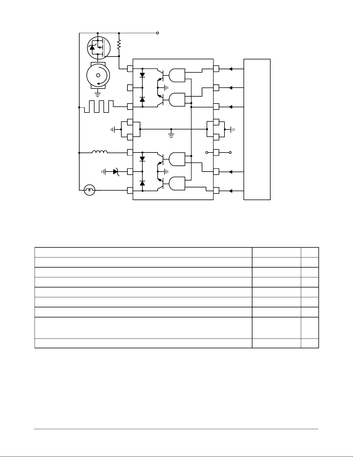
PIN CONNECTIONS
OUTC
MARKING
DIAGRAM
16
NCV7601P
AWLYYWW
1
161
INAOUTA
INBCLAMPAB
ENABLEOUTB
GNDGND
GNDGND
V
CC
INCCLAMPCD
INDOUTD
Semiconductor Components Industries, LLC, 2003
February, 2003 - Rev. 2
ORDERING INFORMATION
Device Package Shipping
NCV7601P
1 Publication Order Number:
DIP-16
25 Units/Rail
NCV7601/D
NCV7601
+14 V
NCV7601
1
A
16
Heater
Solenoid or Relay
30 V
194 Lamp
ABSOLUTE MAXIMUM RATINGS*
2
B
3
4
5
6
ENA
V
CC
15
14
13
12
+5.0 V
11
Controller
C
7
10
D
8
9
Figure 1. Typical Driver Applications
Rating Value Unit
V
CC
-0.3 to 7.0 V
Logic Input Voltage (INA, INB, INC, IND, ENABLE) -0.3 to 15 V
Power Output (OUTA, OUTB, OUTC, OUTD) -0.3 to 60 V
Junction Temperature Range, T
J
-40 to 150 °C
Storage Temperature Range -55 to 150 °C
ESD Susceptibility (Human Body Model) 2.0 kV
Package Thermal Resistance
Junction-to-Case, R
Junction-to-Ambient, R
θ
JC
θ
JA
15
50
Lead Temperature Soldering: Wave Solder (through hole styles only)(Note 1) 260 peak °C
1. 10 second maximum.
*The maximum package power dissipation must be observed.
°C/W
°C/W
http://onsemi.com
2
NCV7601
ELECTRICAL CHARACTERISTICS (4.0 V ≤ V
Characteristic
≤ 5.5 V, -40°C ≤ TJ ≤ 125°C, unless otherwise specified.) Note 2
CC
Test Conditions Min Typ Max Unit
General
V
Supply Current Outputs Off, VCC = 5.5 V
CC
Note 3 I
= 600 mA, VCC = VIN = 5.5 V
OUT
(four outputs on)
(one output on)
-
-
-
-
-
-
5.0
65
20
Output Drivers
I
Saturation Voltage
Leakage Current V
Current Limit 4.5 V < V
= 600 mA, VIN = 2.0 V, VCC = 4.0 V - - 650 mV
OUT
= 60 V, VIN = 0.8 V, VCC = 5.5 V - - 50 µA
OUT
< 16 V, VCC = 5.0 V - - 1.8 A
OUT
Thermal Shutdown - 150 180 210 °C
Sustaining Voltage, V
CE(SUS)
VCC = 5.5 V 40 - - V
Clamp Diodes
Forward Voltage
IF = 1.5 A, VCC = 5.5 V - - 2.0 V
Leakage Current VR = 60 V, VCC = 5.5 V - - 100 µA
Input
Input Current
Input High Voltage I
Input Low Voltage I
0 V ≤ V
OUT
OUT
≤ V
IN
CC
-2.0 - 10 µA
= 600 mA 2.0 - - V
= 600 mA - - 0.8 V
AC Characteristics, Note 4
mA
mA
mA
Turn-On Delay, Turn-Off Delay
I
= 500 mA - - 10 µs
OUT
2. Designed to meet these characteristics over the stated temperature range, though may not be 100% parametrically tested in production.
3. Pulse test.
4. Input rise time ≤ 10 ns, falltime ≤ 10 ns, measured at 50% points.
http://onsemi.com
3

NCV7601
PACKAGE PIN DESCRIPTION
PACKAGE PIN #
DIP-16
1 OUTA Driver A Output.
2 CLAMPAB Diode Clamp to Driver A and Driver B.
3 OUTB Driver B Output.
4 GND Ground.
5 GND Ground.
6 OUTC Driver C Output.
7 CLAMPCD Diode Clamp to Driver C and Driver D.
8 OUTD Driver D Output.
9 IND Driver D Input.
10 INC Driver C Input.
PIN SYMBOL FUNCTION
11 V
12 GND Ground.
13 GND Ground.
14 ENABLE ENABLE Input to all Drivers.
15 INB Driver B Input.
16 INA Driver A Input.
V
CC
INx
ENABLE
18 V
18 V
CC
1.35 V
5.0 V Input Supply Voltage.
+
−
+
V
-
Predriver
= INX • ENA
OUT
X
Thermal Limit
∆T
J
Current Limit
∆I
<< 1.0 Ω
CLAMP
OUTx
Figure 2. Simplified Block Diagram - Each Driver
http://onsemi.com
4

67
NCV7601
TYPICAL PERFORMANCE CHARACTERISTICS
375
65
63
(V)
61
CE(SUS)
V
59
57
55
-40
1.6
1.5
1.4
1.3
(A)
1.2
LIM
I
1.1
1.0
0.9
0.8
-40
-20 0 20 40 60 80 100 120 140
Temperature (°C)
Figure 3. T ypical V
V
V
CE
CE
CE(SUS)
= 4.5 V
= 16 V
-20 0 20 40 60 80 100 120 140
Temperature (°C)
325
I
= 600 mA
275
(mV)
225
175
CE(SAT)
V
OUT
I
OUT
= 400 mA
125
75
25
-40
I
= 100 mA
OUT
-20 0 20 40 60 80 100 120 140
Temperature (°C)
Figure 4. Typical Output On Voltage, VCC = 4.0 V
1.75
1.55
1.35
(V)
F
V
1.15
0.95
0.75
-20 0 20 40 60 80 100 120 140
-40
IF = 1.5 A
IF = 0.5 A
Temperature (°C)
Figure 5. Typical Output Current Limit, V
2.5
2.3
2.1
(mA)
CC
I
1.9
1.7
1.5
-20 0 20 40 60 80 100 120 140
-40
Temperature (°C)
Figure 7. Typical V
Current - No Outputs On,
CC
VCC = 5.5 V
= 5.0 V Figure 6. Typical Clamp Diode Forward Voltage
CC
60
55
50
(mA)
CC
I
45
40
-40
-20 0 20 40 60 80 100 120 140
Temperature (°C)
Figure 8. Typical VCC Current - All Outputs On,
VCC = 5.5 V, I
= 600 mA (Each Output)
OUT
http://onsemi.com
5

NCV7601
TYPICAL PERFORMANCE CHARACTERISTICS
1.37
1.36
1.35
1.34
1.33
(V)
IN
1.32
V
1.31
1.30
1.29
1.28
I
= 100 mA
OUT
I
-20 0 20 40 60 80 100 120 140
-40
Temperature (°C)
Figure 9. Typical Input Threshold Voltage, VCC = 5.0 V
DETAILED OPERATING DESCRIPTION
The NCV7601 Quad Driver consists of four identical
driver sections with output clamp diodes and a common bias
generator.
Each driver input (Figure 2) is buffered by a PNP emitter
follower for r educed i nput b ias c urrent a nd f eatures a n ominal
18 V Zener input clamp for transient protection. Each input
is compared to a separate temperature-compensated
reference, which provides a nominal 1.35 V comparison
threshold. W ith the addition of an external series resistor, the
inputs can be interfaced directly to +14 V automotive system
voltages. Floating inputs are interpreted as high.
Each driver output NPN is supplied with a substantially
fixed base current from the +5.0 V V
pin by a pre-driver.
CC
OUT
= 10 mA
Each pre-driver multiplies a temperature-compensated
reference current when its control input and the common
enable input is high. Current limit and thermal limit circuits
act independently within the pre-driver to reduce base drive
to the output NPN. The independent limit operation allows
the driver to handle inrush current from lamp loads while
protecting the driver from fault conditions that exist long
enough to raise the temperature at that driver to its thermal
limit threshold. Each driver has its own
temperature-sensing device located in close proximity to
the output NPN. The separate sensing devices are
strategically placed at the corners of the die to reduce
interaction between them.
APPLICATIONS INFORMATION
The NCV7601 Quad Driver interfaces high power loads
to low power control signals. The four open-collector
NAND drivers with common ENABLE are TTL, DTL and
CMOS compatible. Any number of drivers may be parallel
connected to drive loads greater than each driver’s nominal
capability. Power for the Quad’s control logic and output
pre-drive is supplied from the +5.0 V V
pin, and is
CC
proportional to the number of active inputs. Minimum
standby power is consumed when the ENABLE input is low.
Each driver is individually protected with current limit and
thermal limit circuitry . Drivers with fault loads are protected
while drivers with normal loads continue to operate,
provided that sufficient heat sinking maintains a good
thermal gradient between all drivers.
Clamp diodes at each driver output provide a means for
managing inductive load transients. The common cathode
pin for each driver pair can be connected to the load supply
voltage for suppression of minor transients resulting from
http://onsemi.com
wiring harness inductances. The use of an external Zener
diode or TVS (T ransient Voltage Suppressor) device such as
the ON Semiconductor 1.5SMCXXXAT3 series is strongly
recommended when driving large inductive loads or when
load supply transients can be expected to exceed the Quad
Driver’s VCE
rating. The use of a TVS device provides
(SUS)
an additional benefit by reducing the decay time of inductive
loads. More information on safeguarding the Quad’s output
NPN’s and about transient suppression methods and device
selection is available in ON Semiconductor application
notes “Understanding Power Transistors Breakdown
Parameters”, document number AN1628/D, “A Review of
Transients and their Means Of Suppression”, document
number AN843/D and “Transient Power Capability of
Zener Diodes”, document number AN784/D. All
application notes are available through the Literature
Distribution Center or via our website at
http://www.onsemi.com.
6

PACKAGE DIMENSIONS
-A-
916
B
18
F
H
G
D
16 PL
0.25 (0.010) T
C
S
SEATING
-T-
PLANE
K
M
A
NCV7601
DIP-16
P SUFFIX
CASE 648-08
ISSUE R
J
M
NOTES:
1. DIMENSIONING AND TOLERANCING PER ANSI
Y14.5M, 1982.
2. CONTROLLING DIMENSION: INCH.
3. DIMENSION L TO CENTER OF LEADS WHEN
FORMED PARALLEL.
4. DIMENSION B DOES NOT INCLUDE MOLD FLASH.
5. ROUNDED CORNERS OPTIONAL.
DIM MIN MAX MIN MAX
L
M
A 0.740 0.770 18.80 19.55
B 0.250 0.270 6.35 6.85
C 0.145 0.175 3.69 4.44
D 0.015 0.021 0.39 0.53
F 0.040 0.70 1.02 1.77
G 0.100 BSC 2.54 BSC
H 0.050 BSC 1.27 BSC
J 0.008 0.015 0.21 0.38
K 0.110 0.130 2.80 3.30
L 0.295 0.305 7.50 7.74
M 0 10 0 10
S 0.020 0.040 0.51 1.01
MILLIMETERSINCHES
http://onsemi.com
7

NCV7601
ON Semiconductor and are registered trademarks of Semiconductor Components Industries, LLC (SCILLC). SCILLC reserves the right to make
changes without further notice to any products herein. SCILLC makes no warranty, representation or guarantee regarding the suitability of its products for any
particular purpose, nor does SCILLC assume any liability arising out of the application or use of any product or circuit, and specifically disclaims any and all
liability, including without limitation special, consequential or incidental damages. “Typical” parameters which may be provided in SCILLC data sheets and/or
specifications can and do vary in different applications and actual performance may vary over time. All operating parameters, including “Typicals” must be
validated for each customer application by customer’s technical experts. SCILLC does not convey any license under its patent rights nor the rights of others.
SCILLC products are not designed, intended, or authorized for use as components in systems intended for surgical implant into the body, or other applications
intended to support or sustain life, or for any other application in which the failure of the SCILLC product could create a situation where personal injury or death
may occur. Should Buyer purchase or use SCILLC products for any such unintended or unauthorized application, Buyer shall indemnify and hold SCILLC
and its officers, employees, subsidiaries, affiliates, and distributors harmless against all claims, costs, damages, and expenses, and reasonable attorney fees
arising out of, directly or indirectly, any claim of personal injury or death associated with such unintended or unauthorized use, even if such claim alleges that
SCILLC was negligent regarding the design or manufacture of the part. SCILLC is an Equal Opportunity/Affirmative Action Employer.
PUBLICATION ORDERING INFORMATION
Literature Fulfillment:
Literature Distribution Center for ON Semiconductor
P.O. Box 5163, Denver, Colorado 80217 USA
Phone: 303-675-2175 or 800-344-3860 Toll Free USA/Canada
Fax: 303-675-2176 or 800-344-3867 Toll Free USA/Canada
Email: ONlit@hibbertco.com
N. American Technical Support: 800-282-9855 Toll Free USA/Canada
http://onsemi.com
JAPAN: ON Semiconductor, Japan Customer Focus Center
2-9-1 Kamimeguro, Meguro-ku, Tokyo, Japan 153-0051
Phone: 81-3-5773-3850
Email: r14525@onsemi.com
ON Semiconductor Website: http://onsemi.com
For additional information, please contact your local
Sales Representative.
NCV7601/D
8
 Loading...