

Page 1
查询NCV7510供应商
NCV7510
FlexMOS Programmable
Peak and Hold PWM
MOSFET Predriver
The NCV7510 high side MOSFET predriver is a fully
programmable automotive grade product for driving solenoids or
other unipolar actuators. The product is optimized for common−rail
diesel fuel injection applications and includes an additional
synchronous clamp MOSFET predriver. Peak and hold currents, peak
dwell time and other features are programmable via the device’s SPI
port. Load current is continuously sampled and compared to the
programmable 7−bit peak/hold DAC values while the load
self−modulates to maintain the desired currents at each of the peak and
hold points. Passive fault diagnostics monitor and protect the
MOSFET s when a fault is detected. Fault data is available via SPI and
an open−drain FAULT output provides immediate fault notification to
a host controller.
The FlexMOS family of products offers application scalability
through choice of external MOSFETs.
Features
• 4 MHz 16−Bit SPI Communication
• 3.3 / 5.0 V Compatible Inputs
• Bootstrap for High Side MOSFET
• Synchronous Clamp Drive
• Cross Conduction Suppression
• Self−Protection
− Overcurrent and Overvoltage
− Antisaturation
• Fault Diagnostics
− Short to Battery/GND
− Open Circuit / Shorted Load
− Overvoltage
• Open−Drain FAULT Output
• Programmable
− Peak / Hold Current PWM Thresholds
− Overcurrent and Overvoltage
− Antisaturation Thresholds
− Peak Dwell Time
• NCV Prefix for Automotive and Other Applications Requiring Site
and Control Changes
Benefits
• Scalable by Choice of MOSFETs
• Reduced Load Power Consumption
• Low Host Controller Overhead
• Low Standby Current
http://onsemi.com
http://onsemi.com
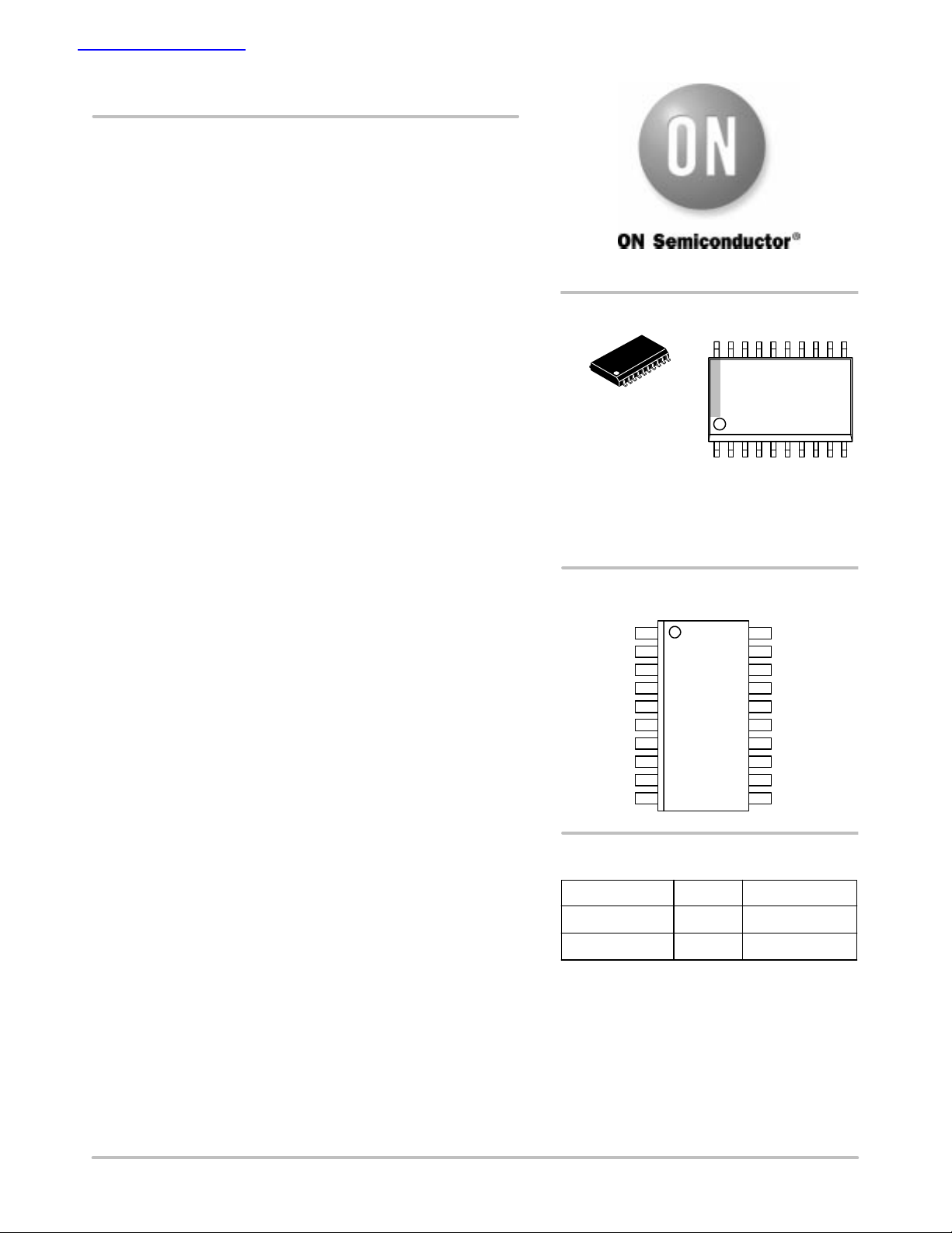
MARKING DIAGRAM
20
20
1
SO−20L
DW SUFFIX
CASE 751D
A = Assembly Location
WL = Wafer Lot
YY = Year
WW = Work Week
PIN CONNECTIONS
120
ENA
CONTROL
PCLK
CSB
SCLK
SI
SO
LOOP
FAULT
OCP
ORDERING INFORMATION
Device Package Shipping
NCV7510DW SO−20L 37 Units/Rail
NCV7510DWR2 SO−20L
†For information on tape and reel specifications,
including part orientation and tape sizes, please
refer to our Tape and Reel Packaging Specification
Brochure, BRD8011/D.
1
NCV7510
AWLYYWW
V
B
DRN
GATE
SRC
CLAMP
PGND
SNS+
SNS−
DGND
V
DD
1000 Tape & Reel
†
Semiconductor Components Industries, LLC, 2005
January, 2005 − Rev. 0
1 Publication Order Number
NCV7510/D
Page 2
NCV7510
ENA
CONTROL
FAULT
CSB
SCLK
SO
PCLK
LOOP
DRN
POROVSD
V
DD
16−BIT
SPI
SI
8−BIT
TIMER
DIAGNOSTICS
VREF
FET
DRIVE
CONTROL
FAULT
7−BIT
DAC
HYSTERETIC
MUX
CONTROL
V
DD
CLAMP
DRIVE
GATE
DRIVE
ANTISAT
DETECTION
OVER
CURRENT
SENSE
AMP
4X
CLAMP
V
B
GATE
SRC
OCP
SNS+
SNS−
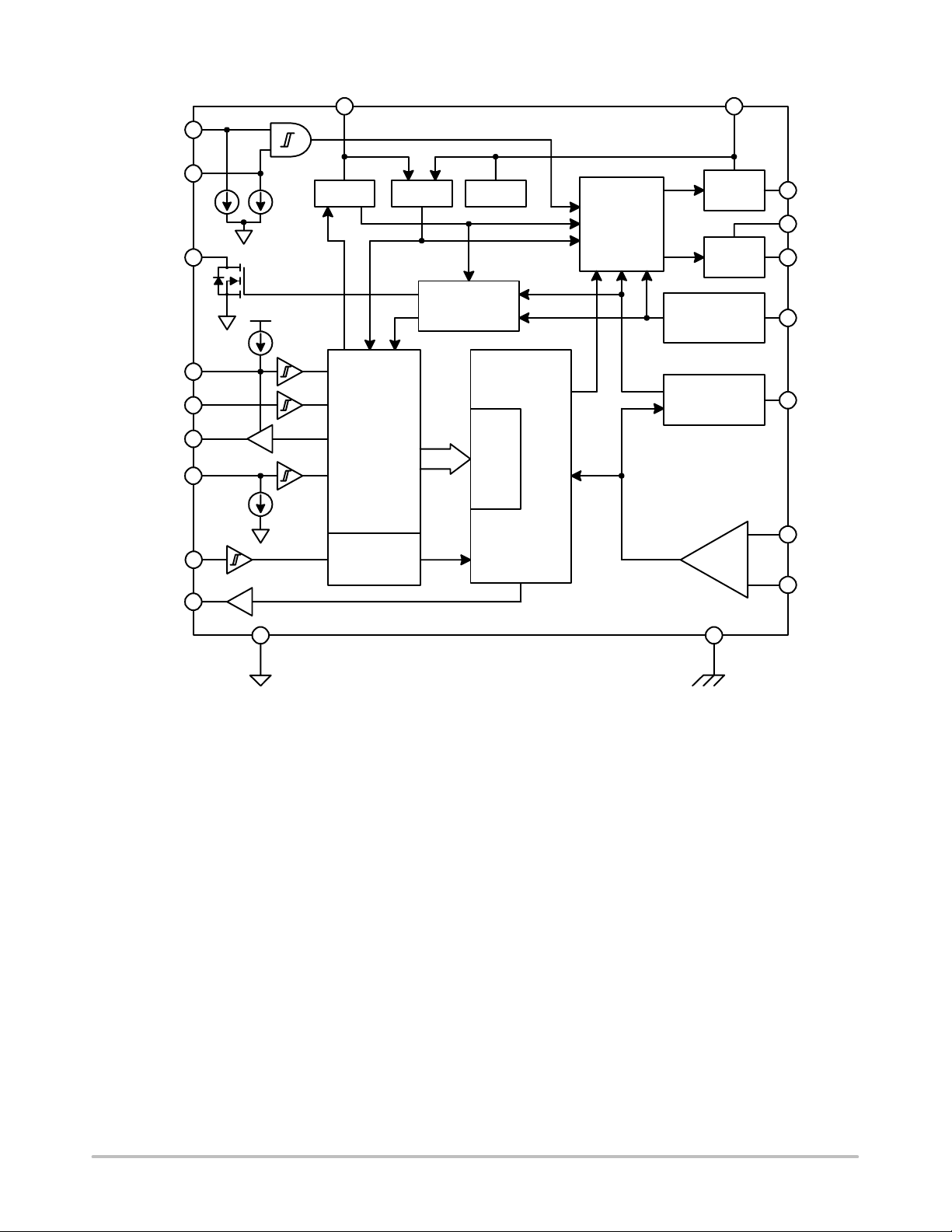
Figure 1. Block Diagram
PGNDDGND
http://onsemi.com
2
Page 3
SPI
HOST CONTROLLER
ENA
CONTROL
PCLK
CSB
SCLK
SI
SO
LOOP
FAULT
NCV7510
VB
DRN
GATE
SRC
CLAMP
PGND
NCV7510
SNS+
SNS−
DGND
BAT
D1
D2D3
RLIM
C
BOOT
M1
NTD32N06
RG
D4
+
MMBZ9V1
M2
NTD32N06
C
BULK2
RS
D5
D6
FILTER
+
C
BULK1
INJECTOR 1
INJECTOR 2
INJECTOR 3
INJECTOR 4
RSNS
NTD32N06
M6
NTD32N06
M5
NTD32N06
M4
NTD32N06
M3
OCP
VDD
RB
RA
RPU
Figure 2. Application Diagram
+5V
http://onsemi.com
3
Page 4
NCV7510
PACKAGE PIN DESCRIPTIONS
PACKAGE PIN# PIN SYMBOL FUNCTION
1 ENA Logic input for Enable.
2 CONTROL Logic input for PWM cycle control.
3 PCLK Logic input for clock or logic level control of Dwell timer.
4 CSB Logic input for active low chip select.
5 SCLK SPI clock input.
6 SI SPI serial data input.
7 SO SPI serial data output.
8 LOOP Control loop state output.
9 FAULT Open−drain fault output.
10 OCP Overcurrent program input.
11 V
12 DGND Supply return; device substrate.
13 SNS− Current sense negative input.
14 SNS+ Current sense positive input.
15 PGND High current supply return; CLAMP antisaturation reference node.
16 CLAMP Clamp MOSFET gate drive output.
17 SRC HS and CLAMP MOSFET antisaturation diagnostic input.
18 GATE HS MOSFET gate drive output.
19 DRN HS MOSFET drain antisaturation / overvoltage diagnostic input.
20 V
DD
B
Logic supply voltage input; CLAMP predriver voltage.
Bootstrapped GATE predriver voltage.
ENA
CONTROL
PCLK
CSB
SCLK
SO
LOOP
FAULT
OCP
120
V
B
DRN
GATE
SRC
CLAMP
SI
PGND
SNS+
SNS−
DGND
V
DD
http://onsemi.com
4
Page 5

NCV7510
Pin Function Descriptions
ENA: CMOS input with hysteresis logically ANDed with
the CONTROL input to command the predriver outputs.
This input has an active pulldown current source.
CONTROL: CMOS input with hysteresis logically ANDed
with the ENA input to command the predriver outputs. This
input has an active pulldown current source.
PCLK: Buffered CMOS input with hysteresis. This input
controls which DAC register pair is selected for load current
comparison. The input is programmed via Auxiliary register
($01) bit D
to respond to a clock signal (AUX D3=0 default
3
at POR) or a logic level (AUX D3=1.) The pin presents a
12 pF maximum load to the controller.
CSB: CMOS input with hysteresis. This input is the
active−low chip select input that enables serial data transfer
between the host controller and the device. This input has an
active pullup current source.
SCLK: Buffered CMOS input with hysteresis. This input
is the synchronizing clock input for serial data transfer
between the micro controller and the device. The pin
presents a 12 pF maximum load to the controller.
SI: Buffered CMOS input with hysteresis. This pin is the
data input to the device’s SPI shift register. Serial data
received at this input is transferred from the host controller
to the shift register under the control of the CSB and SCLK
inputs. The pin presents a 12 pF maximum load to the
controller. This input has an active pulldown current source.
SO: The CMOS compatible line driver at this pin is the data
output from the device’s SPI shift register. Serial data
transmitted at this output is transferred from the shift register
to the host controller under the control of the CSB and SCLK
inputs. The pin is capable of driving 200 pF at 4 MHz and
is HI−Z when the CSB input is high.
LOOP: The CMOS compatible driver at this pin reflects the
state of the control loop. A logic low indicates that load
current is less than the programmed DAC reference.
FAULT: An open−drain low voltage NMOS output at this
pin provides immediate fault indication to a connected host
controller. An external resistor is normally connected
between this pin and V
DD
.
DGND: Device substrate voltage and VDD return path for
mixed signal functions. This pin is the circuit common
reference point.
OCP: This analog comparator input supplies a reference
voltage to the device’s overcurrent fault detection. When the
voltage at this pin is less than 4.5 V, the applied voltage is the
overcurrent reference voltage. When the voltage is greater
than 4.5 V, an internal 3.0 V overcurrent reference is used.
The voltage at this pin must not exceed V
. Applying
DD
approximately VDD + 1.4 V will place the NCV7510 in test
mode and suspend normal operation. The user is advised to
avoid activating the test mode.
V
: +5.0 Vpower supply input. The voltage at this pin
DD
initiates power−on reset, supplies power to internal
mixed−signal functions and supplies gate charge to the
external CLAMP MOSFET. A low ESR external bulk
capacitor connected between VDD and PGND is
recommended to supply transient gate charge. Several
internal reference voltages are derived from V
DD
.
SNS−: The inverting input to the analog current sense
amplifier. This input should be Kelvin connected directly to
the external current sense resistor’s negative terminal.
SNS+: The noninverting input to the analog current sense
amplifier. This input should be Kelvin connected directly to
the external current sense resistor’s positive terminal.
PGND: Return path for the GATE and CLAMP predriver
transient currents and the lower input to the CLAMP
antisaturation detection comparator. This pin should be
star−connected to the CLAMP MOSFET’s source and the
external V
bulk charge capacitor’s negative terminal.
DD
CLAMP: External CLAMP MOSFET predrive output.
This output switches the CLAMP MOSFET’s gate between
V
and PGND.
DD
SRC: Lower input to the GATE antisaturation detection
comparator and upper input to the CLAMP antisaturation
detector.
GATE: External HS MOSFET predrive output. This output
switches the HS MOSFET’s gate between V
and PGND.
B
DRN: Upper input to the GATE antisaturation detection
comparator, overvoltage detection input, and powerup
interlock input. This pin should be connected directly to the
HS MOSFET’s drain terminal.
VB: Bootstrap or boost input voltage. This input supplies
gate charge to the external HS MOSFET.
http://onsemi.com
5
Page 6
NCV7510
MAXIMUM RATINGS (Voltages are with respect to device substrate.)
Rating
DC Supply Voltage (Note 1)
VDRN Peak Transient Voltage (Note 2) VDRN
VB Pin Voltage V
GATE Pin Voltage V
VB to GATE Differential Voltage VB − V
SRC Pin Voltage V
Logic Level Input/Output Voltage
(SO, SI, SCLK, CSB, ENA, CONTROL, PCLK, FAULT, LOOP)
Sense Amplifier Input Voltage
Overcurrent Comparator Input Voltage V
Junction Temperature Tj 150 °C
Storage Temperature Range T
Peak Reflow Soldering Temperature: Lead−free (60 to 150 seconds at 217 °C) (Note 3) 265 peak °C
Maximum ratings are those values beyond which device damage can occur. Maximum ratings applied to the device are individual stress limit
values (not normal operating conditions) and are not valid simultaneously . If these limits are exceeded, device functional operation is not implied,
damage may occur and reliability may be affected.
1. Reverse VDRN protection must be included in the application circuit.
2. VDRN transient voltage suppression must be included in the application circuit.
3. For additional information, see or download ON Semiconductor’s Soldering and Mounting Techniques Reference Manual, SOLDERRM/D,
and Application Note AND8003/D.
Symbol Value Unit
VDRN −0.3 to 45 V
V
V
V
DD
B
GATE
SRC
V
I/O
SNS+
SNS−
OCP
stg
(PK)
GATE
−0.3 to 7.0 V
45 V
−2.0 to 50 V
−2.0 to 50 V
50 V
−2.0 to 45 V
−0.3 to 7.0 V
−0.3 to 45 V
−0.3 to 7.0 V
−0.3 to 7.0 V
−65 to 150 °C
ATTRIBUTES
Characteristic Value Unit
ESD Capability (All Pins)
Human Body Model
Charged Device Model
Moisture Sensitivity (Note 3) MSL 1
Package Thermal Resistance
Junction–to–Ambient, R
Junction–to–Case, R
JA
JC
> 3.0
> 1.0
55
9.0
kV
kV
°C/W
°C/W
http://onsemi.com
6
Page 7
NCV7510
ELECTRICAL CHARACTERISTICS (5 V < V
)
(Note 4
< 26 V, 4.75 V < VDD < 5.25 V, −40°C < TJ < 125°C, unless otherwise specified.)
DRN
Characteristic Conditions Min Typ Max Unit
DRN Input
Input Current
= 12.8 V, VDD = 0 V
DRN
V
= 26 V, VDD =5.25 V
DRN
–
–
0.5
−
5.0
2.0
A
mA
V
Power−On Lockout Threshold VDD = 0 V, GATE predriver locked out – 0.7 1.5 V
Over−Voltage Lockout GATE predriver disabled, CLAMP predriver active
28 32 36 V
Auxiliary Register Bit 6 = 1
Over−Voltage Hysteresis 0.1 0.8 2.0 V
VB Input
Input Bias Current
V
= 24 V – 0.7 1.5 mA
B
VDD Supply
Operating Current
V
= 14 V 3.5 7.0 mA
DRN
Power−On Reset Threshold Predrivers disabled, VDD rising 3.0 3.5 4.4 V
Power−On Reset Hysteresis − 0.25 − V
Digital I/O
High ENA, CONTROL, SI, SCLK, CSB, PCLK 2.2 – – V
V
IN
VIN Low ENA, CONTROL, SI, SCLK, CSB, PCLK – – 0.8 V
VIN Hysteresis ENA, CONTROL, SI, SCLK, CSB, PCLK 0.6 1.2 V
Input Pulldown Current ENA, CONTROL, SI: V
Input Pullup Current CSB: V
SO Low Voltage I
SO High Voltage I
LOOP Low Voltage I
LOOP High Voltage I
LOOP Output Response Delay
(See Figure 3)
SINK
SOURCE
SINK
SOURCE
t
LOOP(HL)
t
LOOP(LH)
FAULT Low Voltage FAULT Active, I
= 0 V −25 – – A
IN
= 1 mA – – 0.4 V
= 1 mA V
= 0.1 mA – – 0.5 V
= 0.1 mA V
; C
LOOP
; C
LOOP
FAULT
= V
IN
DD
= 50 pF
= 50 pF
= 0.5 mA – 0.1 0.5 V
– – 25 A
− 1.0 – – V
DD
− 1.0 – – V
DD
–
–
0.5
0.5
1.2
1.2
s
s
PCLK Input
Input Capacitance
(Note 5) – – 12 pF
Clock Frequency Auxiliary Register Bit 3 = 0 (Note 5) 0 – 20 MHz
DAC Reference Select Delay Auxiliary Register Bit 3 = 1 (Note 5) – – 3.0 s
http://onsemi.com
7
Page 8

NCV7510
ELECTRICAL CHARACTERISTICS (continued) (5 V < VDRN < 26 V, 4.75 V < V
otherwise specified.) (Note 4
)
< 5.25 V, −40°C < TJ < 125°C, unless
DD
Characteristic Conditions Min Typ Max Unit
GATE and CLAMP Predrivers
GATE Output R
GATE Output R
High VB = 7.3 V, VB−V
DS(ON)
Low VB = 7.3 V, V
DS(ON)
GATE Output Delay
(See Figure 4)
GATE Response Delay
(See Figure 4)
GATE Output Low Hold Time
(See Figure 5)
GATE
t
; ENA or CONTROL High to GATE High
P(LH)
C
=2 nF
GATE
t
; ENA or CONTROL Low to GATE Low
P(HL)
C
=2 nF
GATE
t
;SNS+ Falling to GATE Rising
DLY(GR)
VDD=5.0 V, VDRN=10 V, VB=20 V,
V
Following V
SRC
t
;SNS+ Rising to GATE Falling
DLY(GF)
VDD=5.0 V, VDRN=10 V, VB=20 V,
Following V
V
SRC
VDD = 5.0 V, C
= 0.5 V – 20 50
GATE
= 0.5 V – 20 50
– 0.8 1.6 s
– 0.3 0.6 s
– 0.4 1.6 s
, V
GATE
=20% FS, C
DAC
GATE
=2 nF
– 0.4 1.6 s
, V
GATE
=2 nF 5.0 10 15 s
GATE
=80% FS, C
DAC
GATE
=2 nF
GATE Output Pulldown (HI−Z) 20 60 150 k
CLAMP Output R
CLAMP Output R
High VDD = 5.0 V, VDD−V
DS(ON)
Low VDD = 5.0 V, V
DS(ON)
CLAMP
= 0.5 V – 20 50
CLAMP
= 0.5 V – 20 50
CLAMP Output Pulldown 50 200 500 k
CLAMP Output Delay ENA or CONTROL Input Low to CLAMP Output Low;
– – 3.0 s
(Note 5)
Current Sense Amplifier
Input Bias current
Input Common Mode Range V
SNS+, SNS− = 0 V (Each Input) −5.0 − – A
(SNS+,SNS−)
=750 mV −0.3 – 1.0 V
Current Sense Conversion (VDD = 5.0 V)
D/A Resolution
Referred to SNS+, SNS− Inputs 4.70 4.92 5.20 mV
Full Scale Value Referred to SNS+, SNS− Inputs 575 625 675 mV
Differential Non−Linearity – − ±0.75 LSB
DAC Offset DAC Code = 0 −5.0 − 5.0 mV
Trip Point Accuracy DAC Code = 3210 (25% FS) –12.5 − 12.5 mV
DAC Code = 6610 (50% FS) –12.5 − 12.5 mV
DAC Code = 9510 (75% FS) –12.5 − 12.5 mV
DAC Response Delay
(See Figure 6)
t
; CSB Rising to LOOP State Change
DAC
DAC Code = 12710 (Full Scale)
C
= 2 nF (Note 5)
GATE
– − 500 ns
http://onsemi.com
8
Page 9
NCV7510
ELECTRICAL CHARACTERISTICS (continued) (5 V < VDRN < 26 V, 4.75 V < V
otherwise specified.) (Note 4
)
< 5.25 V, −40°C < TJ < 125°C, unless
DD
Characteristic Conditions Min Typ Max Unit
Overcurrent Comparator
V
Input Bias Current
= 3.0 V – 0.26 3.0 A
OCP
Linear Input Voltage Range 1.0 – 3.0 V
Mode Select Threshold VDD = 5.0 V 4.2 4.5 4.8 V
Internal Overcurrent Reference V
Detection Blanking Time
= VDD = 5.0 V 2.7 3.0 3.3 V
OCP
Time to FAULT output low 1.25 2.5 5.0 s
(See Figure 7)
Antisaturation Detect
GATE MOSFET
Auxiliary Register Bit 5 = 0, VDRN−V
Auxiliary Register Bit 5 = 1, VDRN−V
CLAMP MOSFET Auxiliary Register Bit 4 = 0, V
Auxiliary Register Bit 4 = 1, V
SRC Input Bias Current V
Detection Blanking Time
V
SRC
SRC
= 14 V, V
= 0 V, V
GATE
GATE
= 14 V
= 0 V
Time to FAULT output low; GATE or CLAMP 5.0 10 20 s
SRC
SRC
SRC−VPGND
SRC−VPGND
0.96
1.92
0.2
0.4
–
−10
1.20
2.40
0.4
0.8
0.44
–
1.44
2.88
0.6
1.2
4.0
–
V
V
V
V
A
A
(See Figure 8)
Serial Peripheral Interface (VDRN = 14 V, V
SCLK Clock Period
= 5.0 V, Cso = 200 pF) (Figure 9)
DD
250 – – ns
Maximum Input Capacitance Sl, SCLK; (Note 5) – – 12 pF
SCLK High Time f
SCLK Low Time f
Sl Setup Time Sl = 0.8 V/2.0 V to SCLK = 2.0 V
Sl Hold Time SCLK = 2.0 V to Sl = 0.8 V/2.0 V
SO Rise Time (10% VSO to 90% VDD)
SO Fall Time (90% VSO to 10% VDD)
CSB Setup Time CSB = 0.8 V to SCLK = 2.0 V
= 4.0 MHz, SCLK = 2.0 V to 2.0 V 125 – – ns
sclk
= 4.0 MHz. SCLK = 0.8 V to 0.8 V 125 – – ns
sclk
25 – – ns
f
= 4.0 MHz (Note 5)
SCLK
25 – – ns
f
= 4.0 MHz (Note 5)
SCLK
– 25 50 ns
C
= 200 pF (Note 5)
so
– – 50 ns
C
= 200 pF (Note 5)
so
60 – – ns
(Note 5)
CSB Hold Time SCLK = 0.8 V to CSB = 2.0 V
75 – – ns
(Note 5)
SO Delay Time SCLK = 0.8 V to SO Data Valid
f
= 4.0 MHz (Note 5)
SCLK
Transfer Delay Time CSB rising edge to next falling edge.
– 65 125 ns
1.0 – – s
(Note 5)
4. Designed to meet these characteristics over the stated voltage and temperature recommended operating ranges, though may not be 100%
parametrically tested in production.
5. Guaranteed by design.
http://onsemi.com
9
Page 10

NCV7510
)
TIMING WAVEFORMS
CONTROL
GATE
t
P(LH)
50%
20%
80%
t
P(HL)
V
DD
V
B
t
LOOP(HL)
50%
50%
SNS+
LOOP
Figure 3. LOOP Output Response Delay
V
DD
CONTROL
SNS+
V
t
B
HLD
GATE
V
80%
PGND
t
LOOP(LH)
HI−Z
V
DAC(FS)
V
DD
V
SNS+
GATE
CSB
LOOP 50%
DAC(FS)
(DAC CODE =
SI
FULL SCALE OR ZERO)
SNS+
t
DLY(GR)
50%
20%
Figure 4. Gate Output Delay
50%
(DAC CODE =
ZERO OR FULL SCALE)
V
DAC(FS)
V
DLY(GF)
B
V
DD
V
DD
V
DAC(FS)
V
DAC(ZERO
80%
t
t
DAC
Figure 5. Gate Output Low Hold Time
(Gate Switched by CONTROL or SNS+)
V
OCP
SNS+
FAULT
GATE &
CLAMP
(REFERENCE ONLY)
t
OCB
V
50%
DD
Figure 7. Overcurrent Detection Blanking Time
http://onsemi.com
Figure 6. DAC Response Delay
(GATE MOSFET)
(CLAMP MOSFET)
t
ASB
SRC
FAULT
GATE &
CLAMP
V
(DRN−SRC)
V
(SRC−PGND)
(REFERENCE ONLY)
Figure 8. Antisaturation Detection Blanking Time
10
V
50%
V
DRN
V
PGND
DD
Page 11

NCV7510
CSB
SCLK
SI
SO
SI
SETUP
SI
HOLD
CSB
SETUP
1
MSB IN LSB IN
MSB OUT LSB OUT
Note: Not defined but usually MSB of data just received.
BITS 14...1
SO
DELAY
BITS 14...1
Figure 9. SPI Timing
TRANSFER
DELAY
CSB
HOLD
16
SO
RISE,FALL
90% V
10% V
DD
DD
SEE
NOTE
http://onsemi.com
11
Page 12

NCV7510
BASIC OPERATING DESCRIPTION
Introduction
The NCV7510 is designed for use as a predriver for
solenoids or other inductive loads requiring a “peak and
hold” function. It contains all the necessary circuitry for
programming various attributes of the peak and hold events.
These attributes include the current levels of the peak (or
pull−in) event, the current levels of the hold event and the
dwell time of the pull−in event (See Figure 10 Waveforms).
The attribute values are written into appropriate registers in
the NCV7510 via a 16−bit SPI interface. The peak and hold
event is directly initiated and determined by the inputs to the
ENA and CONTROL pins. By applying a logic high level to
these inputs, the user has precise control over how long the
solenoid will be activated.
CONTROL
Input
Solenoid
Current
Dwell
Timer
Programmable Peak
Programmable
Pull−In Time
The dwell time base for the pull−in event is provided to the
IC’s PCLK input by the user, and may be programmed by a
register bit to either be derived from a clock signal or be level
controlled. When driven by a clock signal, the drive mode
will automatically change from the peak to the hold event
when the dwell time expires. When level controlled, the
drive mode will change according to the logic state of the
PCLK input. Bringing the ENA or CONTROL input low
before the dwell time expires will terminate the peak event
and turn off the predrivers. Figure 10 shows the general
behavior of the NCV7510.
Programmable Hold
GATE
Predrive
CLAMP
Predrive
Figure 10. Idealized Waveforms
http://onsemi.com
12
Page 13

NCV7510
BASIC OPERATING DESCRIPTION (continued)
Hysteretic Control
The NCV7510 employs hysteretic control to achieve the
programmed peak and hold currents. The IC measures the
load current via an external sense resistor (See Functional
Block Diagram on page 2 and Application Diagram on
page 3). This voltage is applied to a differential amplifier’s
SNS+ and SNS− inputs. The amplified signal is then
compared to the programmed peak and hold reference levels
generated from the 7−bit D/A converter. (Refer to Figure 1 1)
During the peak event, the load current is compared to the
programmed values in the peak high and peak low registers
for the duration of the programmed dwell time. The
hysteretic controller will switch between the programmed
peak high and peak low values at a PWM rate determined by
the load supply voltage, the load characteristics, the peak
and valley current levels, and the response times of the
NCV7510 and external MOSFETs. When the dwell time h as
been reached, the controller will select the programmed
values in the hold high and hold low registers and the load
current will then be compared to these values. The hysteretic
PWM rate for the hold event is dependent on the same
factors as the peak event.
16−Bit
SPI
Registers
5−Bit Fault
7−Bit Peak High
7−Bit Hold High
7−Bit Peak Low
7−Bit Hold Low
7−Bit Auxiliary
8−Bit Dwell
MUX
MUX
Down
Counter
When the ENA and CONTROL inputs are brought high,
the dwell timer is initialized and the MOSFET drive control
circuit selects the GATE predrive output, activating the high
side MOSFET and allowing current to increase in the load.
When the peak high current level is reached, the MOSFET
drive control circuit will turn off the GATE predrive and then
turn on the CLAMP predrive. With the high side MOSFET
turned off, current in the load will begin to decrease. When
the peak low current level is reached, the MOSFET drive
control circuit will turn off the CLAMP predrive and then
turn on the GATE predrive. The peak event may be
terminated before the end of the programmed dwell time by
bringing either the ENA or CONTROL input low.
Otherwise, the peak high/low cycle repeats for the duration
of the peak dwell time.
Once the peak dwell time has been reached, the hysteretic
MUX control circuit will switch from the peak high and peak
low registers and now use the hold high and hold low
registers. Operation in this mode is quite the same as
described above for the peak event, except that the
programmed hold currents are now used to reduce power
dissipation in the load. The complete peak and hold event is
terminated when ENA or CONTROL is brought low.
V
BAT
V
R
A
R
B
7−Bit
DAC
Peak/Hold
Comparator
Overcurrent
Comparator
C2
3V REF
Sense
Amp
OCP
Select
C3
V
DD
GATE
Predriver
CLAMPC1
A1
4.5V
V
B
DD
OCP
L
R
SNS
PCLK
÷20
Prescaler
Figure 11. Hysteretic MUX Control Block Diagram
http://onsemi.com
13
Page 14

NCV7510
DETAILED OPERATING DESCRIPTION
Power Up/Down Control
The NCV7510 powerup control prevents spurious output
operation by interlocking the V
supplies. At the system level, it is assumed that the V
and VDD power
BAT
BAT
voltage is available before the VDD voltage. The Power−On
Reset (POR) interlock circuit derives an output disable
signal from the V
voltage at the DRN input and causes
BAT
the GATE and CLAMP outputs to be kept at the PGND
potential. Application of the VDD power supply allows the
outputs to subsequently be enabled when the VDD voltage
exceeds the POR threshold. All internal registers are then
initialized to their default states, fault data is cleared and the
GA TE and CLAMP outputs are held low (external MOSFET
V
approximately 0 V.) When the VDD voltage falls below
GS
the POR threshold during power down, the GATE and
CLAMP outputs are driven and held low until V
BAT
falls
below about 1.2 volts.
SPI Communication
The NCV7510 is a 16−bit SPI slave device. Fault data is
simultaneously sent from the device’s SO pin while
command data is received at the SI pin under synchronous
control of the master’s SCLK signal. No parity or buffer
under/over run detection circuitry is employed; therefore a
valid CSB frame must contain exactly 16 SCLK cycles for
each CSB high–low–high transition.
The host initiates communication when the CSB input is
driven low. Present fault data is latched in the device’s SPI
shift register when CSB goes low. Fault data, sent MSB first
at the SO output, changes on the falling edge of SCLK and
is guaranteed valid before the next rising edge of SCLK. The
data at the SI input is received MSB first and must be valid
before the rising edge of SCLK. The 16 bits received at the
SI input before CSB is driven high will be translated as the
current command.
SPI communication between the host and the NCV7510
may either be parallel via individual CSB addressing or
daisy−chained through other devices using a compatible SPI
protocol.
Command and Register Structure
The 16−bit command data received by the NCV7510 is
decoded into 8−bit address and 8−bit data words. The upper
byte, beginning with the received MSB, is bit−wise decoded
to address one of six internal registers and the lower byte is
decoded into program data for the addressed register. A
dummy address ($00) can also be sent to retrieve fault data.
Note that the register addresses are not fully decoded.
Sending an address combining more than one address bit
will result in the same data being sent to more than one
register. Bits A
and A
7
select internal test modes and should
6
always be set to 0. Figure 12 describes the general 16−bit SPI
word format and valid register addresses. Each register is
next described in detail.
MSB LSB
A7A6A5A4A3A2A1A0D7D6D5D4D3D2D1D
ADDRESS DATA
$01 AUX
$02 HDLO
$04 HDHI
$08 PKLO
$10 PKHI
$20 DWELL
Figure 12. 16−bit SPI Word Format and Valid Register
Auxiliary Register [$01]
D7D6D5D4D3D2D1D
D7D6D5D4D3D2D1D
D7D6D5D4D3D2D1D
D7D6D5D4D3D2D1D
D7D6D5D4D3D2D1D
D7D6D5D4D3D2D1D
Addresses
0
0
0
0
0
0
0
The AUX register is used to program several diagnostic
features and the behavior of the dwell timer under control of
the PCLK input and the DWELL timer register. This
register is initialized to $00 at POR. Bit definitions are
shown for this register in Figure 13.
$01 AUX
D7D6D5D4D3D2D1D
Figure 13. AUX Register Bit Definitions
0
DWELL TIME PRE−SCALE
PCLK INPUT MODE
CLAMP ANTI−SAT THRESHOLD
GATE ANTI−SA T THRESHOLD
OVERVOLTAGE ENABLE
Bit D7 selects an internal test mode and should always be
set to 0. Bit D6 controls interruption of load current by the
overvoltage detection function. At POR, the overvoltage
interrupt function is disabled. Programming D
=1 enables
6
overvoltage interrupt and will cause the FAULT output to
respond to an overvoltage event. Overvoltage events are
reported via the SPI shift register regardless of the state of
AUX D
.
6
http://onsemi.com
14
Page 15

NCV7510
DETAILED OPERATING DESCRIPTION (continued)
Bits D5 and D4 program the respective antisaturation
detection thresholds for the GATE (high side) and CLAMP
MOSFET s. A t POR, the GATE threshold is nominally set to
1.2 V and the CLAMP to 0.4 V . Programming the respective
bits to 1 nominally sets the GATE threshold to 2.4 V and the
CLAMP to 0.8 V.
Bit D
selects the functional mode for the PCLK input. At
3
POR, D3=0 and the PCLK input is configured to accept a
clock signal as the time base for an internal programmable
dwell timer. The dwell timer determines when to change
modes from peak to hold. Setting D
=1 configures the
3
PCLK input to accept a logic−level input which then directly
controls the selection of the peak or hold mode. When D3=1,
PCLK=0 selects the peak mode and PCLK=1 selects the
hold mode.
Bits D
program the dwell timer prescaler to divide
2−D0
the incoming clock signal at the PCLK input when AUX bit
D3=0. Refer to the Dwell Timer register description for
additional programming details.
Peak/Hold DAC Registers [$10,$08,$04,$02]
The peak and hold registers program the DAC reference
pairs for the peak and hold load currents. Each 8−bit register
uses only the 7 lower bits, and bit 8 must always be set to 0.
At POR, the registers are set to $00.
The PKHI ($10) and PKLO ($08) register pair contents
are the DAC reference values used during the peak mode of
the control cycle. The HDHI ($04) and HDLO ($02) register
pair contents are the DAC reference values used during the
hold mode of the control cycle. The peak or hold mode is
determined by the state of the internal dwell timer or the
logic level at the PCLK input. Refer to the AUX register and
Dwell Timer register descriptions for additional details. The
register values for the load currents can be determined with
the following equation:
IL R
VAL
10
where IL is the desired load current, R
SNS
4.92 mV
LSBs
is the current sense
SNS
(eq. 1)
resistor, and 4.92 mV is the nominal D/A resolution. The
maximum value of load current that can be programmed for
a given R
resistor can be found by:
SNS
I
L(MAX)
625 mV
R
SNS
(eq. 2)
where 625 mV is the nominal D/A full−scale value.
Dwell Time Register [$20]
The 8−bit dwell timer register value determines when the
programmed DAC reference pairs change from the peak
mode to the hold mode. Dwell timer operation is also
dependant upon the value of AUX register bits D
3−D0
(refer
to the Auxiliary register description.) Figure 14 shows a
detailed block diagram of the dwell timer.
$01 D7D6D5D4D3D2D1D
PCLK
÷20
4−20MHz Clock
(10µS Time Base)
$20 D7D6D5D4D3D2D1D
Down Counter
Figure 14. Dwell Timer Block Diagram
3−bit
Prescale
Divider
8−bit
0
Peak
Dwell
Time
0
When AUX D3=0, the dwell timer register value is
combined with the AUX D
prescale value to generate
2−D0
a dwell time based on the clock signal applied to the PCLK
input. The timer is designed to produce dwell times from 0
to 2.55 ms with 10 s resolution for popular host controller
clock rates. Figure 15 illustrates the prescale divisor truth
table for some common clock rates.
$01 D
D6D5D
7
÷
Figure 15. AUX Register Prescale Divisors
÷
÷
÷
÷
÷
÷
÷
10
2
3
4
5
6
7
8
D3D2D1D
4
0 0 0 0
0 0 0 1
0 0 1 0
0 0 1 1
0 1 0 0
0 1 0 1
0 1 1 0
0 1 1 1
1 X X XDIRECT IN
PCLK (MHz)
0
4.0
6.0
8.0
10.0
12.0
14.0
16.0
20.0
Logic Level
A general formula for determining dwell time based on
the clock frequency applied to the PCLK input is:
where t
(
DIV 20 N
t
DWELL
DWELL
PCLK
is the dwell time in s, DIV is the pre−scale
10
)
20
(eq. 3)
divisor, PCLK is the clock frequency in MHz, and N10 is the
content of the DWELL time register.
Fault Reporting
When a fault occurs, the open−drain FAULT flag is
latched low and fault information is latched and transferred
into the SPI shift register while CSB is high.
The host controller initiates SPI communication when
CSB goes low, and current fault information can then be
shifted out of the NCV7510’s SO output. While CSB is low,
transfer of new fault information is blocked. The FAULT
flag and fault data are cleared by the rising edge of CSB.
http://onsemi.com
15
Page 16

NCV7510
DETAILED OPERATING DESCRIPTION (continued)
Bits D4−D0 of the 16−bit SO word indicate detected faults
such that DX = 1 when a fault is detected. Figure 16 describes
the fault bit definitions. At POR, the register bits are cleared
to $00. Refer to the Fault Diagnosis description for details
regarding the NCV7510’s fault strategies and behaviors,
discussed in the next section.
SO FAULT DATA
OVERVOLTAGE
SHORT TO GND SHORT TO BATTER Y
D15− D5 = DON’T CARE; D4 − D0: 1 = FAULT, 0 = NO FAULT
Figure 16. SO Fault Bit Definitions
D4D3D2D1D
OVERCURRENT
0
OPEN LOAD
Fault Diagnosis and Protection Behavior
General
The NCV7510 continuously monitors the load supply
voltage, external MOSFETs, the load current, and the
control loop state during a control cycle for fault conditions.
Faults are managed on a cycle−by−cycle basis with regard
to the CONTROL and ENA inputs and are recoverable
(automatic fault re−try) such that the NCV7510 will attempt
to properly drive the load during the next control cycle.
Attention is focused on faults that may cause destructive
failure of the load, the external MOSFETs, or the sense
resistor.
Overcurrent faults are detectable regardless of the
CONTROL and ENA input states. Short to battery and short
to GND (antisaturation) faults are detectable when the
CONTROL and ENA inputs are high. Destructive fault
types are managed when possible to prevent failure by
latching both predriver outputs off. Fault reporting for these
types is priority encoded such that the first detected fault
locks out subsequent fault reporting bits. These faults cause
the FAULT flag to be set and latched low.
Non−destructive open load faults require no intervention
and are detectable at the end of a control cycle when
CONTROL or ENA goes low. This fault type has no priority
and is reported if no other fault has been detected, and does
not set the FAULT flag.
Overvoltage faults are detected without regard to the
CONTROL and ENA inputs. Management, reporting and
FAULT flag behavior for this fault type is dependent upon
the state of AUX register bit D
.
6
Reset of fault protection, and clearing of fault data and the
FAULT flag are independent. Protection circuitry is reset on
the rising edge of either the CONTROL or ENA inputs.
Fault data and the FAULT flag are cleared by the rising edge
of CSB. At power−on reset, all fault protection, fault data,
and the FAULT flag are cleared.
Fault detection, protection and reporting are detailed in
the following sections and are summarized in Table 1.
Overvoltage
The load supply voltage is monitored at the DRN pin for
overvoltage faults, and fault detection occurs regardless of
the states of CONTROL and ENA inputs. The interruption
of load current by the overvoltage detection circuit can be
programmed by bit D
in the AUX register. At POR, the
6
overvoltage interrupt default state is disabled (AUX D6=0).
When AUX D
=0 an overvoltage fault has no priority and
6
is reported if no other fault has been detected. The predrivers
and the FAULT flag are unaffected.
Programming AUX D6=1 enables overvoltage interrupt.
When CONTROL and ENA are high, an overvoltage fault
will cause the GATE output to be latched off, the CLAMP
output to be latched on, and the FAULT flag to be latched
low. The fault is given reporting priority and locks out
subsequent fault reporting bits. Overvoltage protection is
reset when CONTROL or ENA is brought low and then high
again.
Avalanche of the high side (HS) MOSFET may occur
when the CLAMP MOSFET is on during an overvoltage
fault (overvoltage enabled.) Avalanche of both the HS and
CLAMP MOSFETs may occur (overvoltage disabled) if the
overvoltage amplitude exceeds the combined avalanche
voltages of both MOSFETs. The devices should be carefully
chosen for proper avalanche voltage and avalanche energy
rating suitable to the application and its operating
environment.
Note that the NCV7510 requires transient overvoltage
suppression in accordance with the specifications in the
Maximum Ratings table.
Overcurrent
Load current (converted to a voltage by external sense
resistor R
) is monitored at the SNS+ and SNS−
SNS
differential inputs. A fault is detected when the amplified
differential voltage exceeds the overcurrent reference. A
nominal 2.5 s filter is used to help prevent false overcurrent
detection.
Overcurrent detection occurs regardless of the states of
the CONTROL and ENA inputs. This fault has reporting
priority and will latch the FAULT flag low. If overcurrent is
detected when CONTROL and ENA are high, both GATE
and CLAMP outputs are latched off. Overcurrent protection
is reset when the CONTROL or ENA input is brought low
and then high again.
http://onsemi.com
16
Page 17

NCV7510
DETAILED OPERATING DESCRIPTION (continued)
An overcurrent comparator input pin (OCP) is provided to
program a current limit reference value. When the voltage
at the OCP input is less than 4.5 V, the applied voltage is the
overcurrent reference voltage. When the voltage is greater
than 4.5 V, an internal 3.0 V overcurrent reference is used.
The voltage at OCP pin must not exceed V
approximately VDD + 1.4 V will place the NCV7510 in test
mode and suspend normal operation. The user is advised to
avoid activating the test mode.
The OCP reference can be programmed via an external
voltage divider placed between the V
illustrated by resistors RA and RB in the Hysteretic MUX
Block and Application diagrams. The following formulas
can be used to dimension the resistors:
V
RA R
I
OC
where 4 is the nominal sense amplifier gain and R
external load current sense resistor.
Overcurrent faults may be detected when the load is
shorted, when the SNS+ input is shorted to V
sense resistor is open, or when the peak or hold currents are
programmed higher than the overcurrent reference.
Open−circuit failure of the sense resistor may produce
voltages in excess of the NCV7510’s SNS+ input Maximum
Rating. This condition can be avoided by series connection
of a pair of diodes across the sense resistor (see Application
Diagram – D5 , D 6 ) t o p r o v i d e a p a t h f or the l o a d c urrent. The
diodes must be capable of carrying the maximum expected
load current and should be energy−rated for the application.
Open Load
To maintain the scalable flexibility of the NCV7510, the
states of the CLAMP predriver output and the ENA and
CONTROL inputs are monitored to determine an open load
condition as opposed to the detection of an absolute value of
minimum load current. It is expected that during normal
operation, a state change will occur at the CLAMP output as
a result of load current modulation between the peak high
and peak low program points while ENA and CONTROL
are high. Open load detection relies on the occurrence of a
control loop state change before the ENA or CONTROL
input goes low.
B
IOC 4 R
RA R
DD
R
B
B
and DGND pins, as
DD
SNS
V
DD
4 R
SNS
1
. Applying
DD
BAT
(eq. 4)
(eq. 5)
is the
SNS
, when the
If a control loop state change has not occurred during the
time that ENA and CONTROL were high, an open load fault
is detected. When an open load fault is detected, no
intervention is required. This fault type has no priority and
is reported if no other fault has been detected, and does not
set the FAULT flag. Open load fault data is cleared by the
rising edge of CSB.
Open load faults may be detected when the load is open,
when the sense resistor is shorted, or when the load current
is unable to reach the programmed peak or hold high current
value.
False open load faults may be indicated during engine
cranking when battery voltage can initially dip to about 5−6
volts. The programmed current may not be reached and a
state change in the control loop may not occur, thus
producing a false open load indication.
Antisaturation
Each of the high side and clamp MOSFET’s
drain−to−source voltages is separately monitored and
compared to an independently programmable saturation
detection threshold voltage. The detection thresholds are
programmed via the AUX D
the thresholds default nominally to 1.2 V for the high side
MOSFET and to 0.4 V for the clamp MOSFET. Setting
AUX D
threshold to nominally 2.4 V. Similarly, setting AUX D4=1
programs the clamp antisaturation detection threshold to
nominally 0.8 V. Each of the antisaturation detectors
employs a nominal 10 s filter to help prevent false anti−sat
fault detection.
circuitry monitors the voltage between the DRN and SRC
pins (high side) if the GATE output is on and monitors the
voltage between the SRC and PGND pins if the CLAMP
output is on.
ground fault at the SRC pin exists. Clamp saturation may be
detected when a short to battery fault at the SRC pin exists.
The GATE and CLAMP outputs are latched off and the
FAULT flag is set if either of these faults is detected.
that the first detected fault locks out subsequent fault
reporting bits. Antisaturation protection is reset when the
CONTROL or ENA input is brought low and then high
again.
=1 programs the high side antisaturation detection
5
When CONTROL and ENA are high, the antisaturation
High side saturation may be detected when a short to
Fault reporting for these types is priority encoded such
and D4 register bits. At POR,
5
http://onsemi.com
17
Page 18

NCV7510
DETAILED OPERATING DESCRIPTION (continued)
T able 1. Fault Types, Management and Reporting
Fault Type
CONTROL ENA AUX D
Overcurrent X X X OFF OFF D0 YES YES
Open Load HL 1 X OFF OFF D1 NO NO 1
Short to BAT 1 1 X OFF OFF D2 YES YES 2
Short to GND 1 1 X OFF OFF D3 YES YES 3
Overvoltage
†Output states after detection of a fault. Protection is reset on the rising edge of the CONTROL or ENA inputs.
‡ Fault data and the flag are cleared by the rising edge of the CSB input.
1. If detected, fault is reported after the falling edge of the CONTROL (or ENA) input.
2. Detection via CLAMP antisaturation.
3. Detection via GATE antisaturation.
4. When AUX D
= 0, overvoltage will be reported along with priority faults; outputs are unchanged.
6
Input States †Output States ‡Fault Data
GATE CLAMP Report Bit Priority
6
X X 0 — —
0 1 1 OFF OFF YES YES
1 1 1 OFF ON YES YES
D4
NO NO 4
‡FAULT
Flag Set
Note
http://onsemi.com
18
Page 19

NCV7510
DETAILED OPERATING DESCRIPTION (continued)
Operational Behavior
General
The NCV7510 is designed to maintain the programmed
load current at the PKHI and PKLO or at the HDHI and
HDLO reference values. While the device’s flexibility
allows all of these to be programmed to the same value, a
non−zero value is nonetheless required and the minimum
value is constrained by the NCV7510’s DC and AC
capabilities. It is also possible to reverse the order of the
PKHI|PKLO and HDHI|HDLO register values such that the
HI value is less than the LO value. While this is unlikely to
result in damage to the application, it will certainly lead to
bizarre behavior.
As previously noted, the PKHI program value may not be
reached during engine cranking when battery voltage may
initially dip to about 5−6 volts, particularly when driving
low resistance loads. This has additional implications for
both the external bootstrap circuitry (duty cycle 100%)
and open−load detection behavior, both of which are
discussed in other sections of this data sheet.
The NCV7510’s ability to maintain the programmed load
currents is constrained by the total of the NCV7510’s
inherent DC accuracy and loop response delay, the load
characteristics, and any additional delays imposed by
external compensation circuitry, whether slew−rate limiting
or other filtering designed to attenuate the egress or ingress
of radiated or conducted EMI.
Mode Control
The dwell timer selects which pair of the peak or hold
registers is setting the internal DAC and thus determines
whether the device is operating in the peak mode or the hold
mode. Bit D
of the AUX register determines whether a
3
logic level at the PCLK input directly controls the dwell time
or whether the internal dwell timer divides down an external
clock signal at the PCLK input.
When AUX D
=1, the control loop will be placed in the
3
peak mode when PCLK=0 and in the hold mode when
PCLK=1. When AUX D3=0, the control loop state will be
determined by the state of the dwell timer. The dwell time is
programmed via prescale divisor AUX register bits D
2−D0
and by the 8−bit DWELL timer register.
In the following sections, “dwell timer” means either the
state of the logic level at the PCLK input or the state of the
internal dwell timer.
Output Control
The state of the GATE and CLAMP outputs is determined
by the ENA and CONTROL inputs and by the state of the
control loop. In the absence of any faults, the state of the
control loop is determined by the contents of the peak and
hold registers, the state of the dwell timer , and the magnitude
of the load current.
The output control cycle begins when both the ENA and
CONTROL logic inputs are asserted high and ends when
either input is asserted low. At the beginning of each control
cycle the dwell timer and protection circuitry are initialized,
and the internal DAC is initialized to the PKHI register value
(if the dwell time register content is non−zero or if AUX
D
=1 and PCLK=0) or to the HDHI register value (if the
3
dwell time register content is null or if AUX D3=1 and
PCLK=1). The GATE and CLAMP output states will be
determined by the state of the control loop. At the end of
each control cycle the GATE and CLAMP outputs are driven
low, the dwell timer is reset, and open load fault data is
transferred into the SPI shift register if an open load fault
exists.
Control Loop
Load current is converted to a voltage via an external
sense resistor and compared with the programmed internal
DAC voltages. During the dwell time, the load current is
compared to the DAC voltages set by the peak high and peak
low register values. When the dwell time expires, the load
current is compared to the DAC voltages set by the hold high
and hold low register values. The state of the control loop is
reflected at the LOOP output such that a logic low indicates
that load current is less than the programmed DAC
reference.
When the load current is less than the peak or hold high
current, the GATE output is at the V
potential and the
B
CLAMP output is at PGND. When the load current is greater
than the peak or hold HI current, the DAC voltage is set to
the peak or hold LOW register value, the GATE output is
driven to PGND and the CLAMP output is driven to V
DD
When the load current is less than the peak or hold low
current, the DAC voltage is set to the peak or hold HIGH
register value, the GATE output is driven to VB and the
CLAMP output is driven to PGND.
.
http://onsemi.com
19
Page 20

NCV7510
DETAILED OPERATING DESCRIPTION (continued)
MOSFET Predrivers
The NCV7510 employs cross−conduction suppression
for the external high side and clamp MOSFETs. The
CLAMP antisaturation circuitry is used to detect the
turn−off of the high side MOSFET and the voltage at the
CLAMP pin is monitored to detect turn−off of the CLAMP
MOSFET. Figure 17 shows the simplified predriver circuits.
The high side predriver is designed to allow external
system level diagnostics to be implemented at the SRC pin.
The driver is constructed to provide a typical 20 discharge
path for 10 s at turn−off and a 60 k gate−source bleed
resistance to help prevent MOSFET turn−on from leakage
or noise. The R
resistor must be carefully chosen to ensure
G
full depletion of the high side MOSFET’ s gate char ge in less
than 10 s.
Current for the GATE predrive output is supplied from the
V
voltage developed by an external bootstrap circuit or
B
boost power supply. Current for the CLAMP predrive output
is supplied from the VDD power supply.
While the IC contains no slew rate control circuitry, slew
rate control of the high side MOSFET can be achieved by the
use of a series gate resistor (R
.) Since the body diode of the
G
CLAMP MOSFET conducts the load current immediately
after high side turn off, slew rate control of the CLAMP
MOSFET gives no benefit and the use of a series gate
resistor will interfere with cross−conduction suppression.
Bootstrap Circuit
A bootstrap circuit can be constructed using a diode,
resistor, and capacitor to generate the VB voltage necessary
to put the external high side MOSFET in full conduction
(refer to Figure 17). The circuit charges C
and R
when the SRC pin is low. The charge is then
LIM
BOOT
through D2
transferred to the high side MOSFET when M1 in the GATE
predriver is turned on, and the capacitor rides up with the
voltage at the SRC pin. The charge is continually refreshed
as a result of alternate switching of the high side and clamp
MOSFET s. A clamp diode at the V
input (see Application
B
Diagram – Diode D3) may be needed to keep the NCV7510
within its maximum ratings during overvoltage transients.
D4 ensures that the high side MOSFET’s maximum VGS is
not exceeded (refer to Figure 17).
While simple and straightforward in operation, a
bootstrap circuit depends on periodic refresh and thus
cannot run at 100% duty cycle. During engine cranking, the
PKHI program value may not be reached and a state change
in the control loop may not occur, possibly fully depleting
(and preventing recharge) of the bootstrap capacitor.
With the use of logic−level MOSFETs and careful design,
sufficient V
should be available during start up. Attention
GS
to leakage paths (such as external gate−source bleed
resistors) and the VB input bias current will help ensure that
gate charge is available when recharge does not occur.
VBAT
V
B
I
M3
VB
60 k
M4
M5
20
20
M1
20
M2
20
V
DD
200 k
C
BOOT
GATE
R
SRC
CLAMP
PGND
G
IN
10 s
Q
D2
R
LIM
M
HS
D4
L
SOL
R
SOL
M
CL
R
SNS
Figure 17. Simplified GATE and CLAMP Predrivers
http://onsemi.com
20
Page 21

NCV7510
PACKAGE DIMENSIONS
SO−20L
DW SUFFIX
CASE 751D−05
ISSUE G
H10X
M
B
M
0.25
D
20
1
B20X
M
SAS
T
0.25
18X
e
A
11
E
10
h X 45
B
B
A
SEATING
PLANE
A1
T
NOTES:
1. DIMENSIONS ARE IN MILLIMETERS.
2. INTERPRET DIMENSIONS AND TOLERANCES
PER ASME Y14.5M, 1994.
3. DIMENSIONS D AND E DO NOT INCLUDE MOLD
PROTRUSION.
4. MAXIMUM MOLD PROTRUSION 0.15 PER SIDE.
5. DIMENSION B DOES NOT INCLUDE DAMBAR
PROTRUSION. ALLOWABLE PROTRUSION
SHALL BE 0.13 TOTAL IN EXCESS OF B
DIMENSION AT MAXIMUM MATERIAL
CONDITION.
MILLIMETERS
DIM MIN MAX
A 2.35 2.65
A1 0.10 0.25
B 0.35 0.49
C 0.23 0.32
D 12.65 12.95
E 7.40 7.60
e 1.27 BSC
L
C
H 10.05 10.55
h 0.25 0.75
L 0.50 0.90
0 7
http://onsemi.com
21
Page 22

NCV7510
FlexMOS is a trademark of Semiconductor Components Industries, LLC.
ON Semiconductor and are registered trademarks of Semiconductor Components Industries, LLC (SCILLC). SCILLC reserves the right to make changes without further notice
to any products herein. SCILLC makes no warranty, representation or guarantee regarding the suitability of its products for any particular purpose, nor does SCILLC assume any liability
arising out of the application or use of any product or circuit, and specifically disclaims any and all liability, including without limitation special, consequential or incidental damages.
“Typical” parameters which may be provided in SCILLC data sheets and/or specifications can and do vary in different applications and actual performance may vary over time. All
operating parameters, including “Typicals” must be validated for each customer application by customer’s technical experts. SCILLC does not convey any license under its patent rights
nor the rights of others. SCILLC products are not designed, intended, or authorized for use as components in systems intended for surgical implant into the body, or other applications
intended to support or sustain life, or for any other application in which the failure of the SCILLC product could create a situation where personal injury or death may occur. Should
Buyer purchase or use SCILLC products for any such unintended or unauthorized application, Buyer shall indemnify and hold SCILLC and its officers, employees, subsidiaries, affiliates,
and distributors harmless against all claims, costs, damages, and expenses, and reasonable attorney fees arising out of, directly or indirectly, any claim of personal injury or death
associated with such unintended or unauthorized use, even if such claim alleges that SCILLC was negligent regarding the design or manufacture of the part. SCILLC is an Equal
Opportunity/Affirmative Action Employer. This literature is subject to all applicable copyright laws and is not for resale in any manner.
PUBLICATION ORDERING INFORMATION
LITERATURE FULFILLMENT:
Literature Distribution Center for ON Semiconductor
P.O. Box 61312, Phoenix, Arizona 85082−1312 USA
Phone: 480−829−7710 or 800−344−3860 Toll Free USA/Canada
Fax: 480−829−7709 or 800−344−3867 Toll Free USA/Canada
Email: orderlit@onsemi.com
N. American Technical Support: 800−282−9855 Toll Free
USA/Canada
Japan: ON Semiconductor, Japan Customer Focus Center
2−9−1 Kamimeguro, Meguro−ku, Tokyo, Japan 153−0051
Phone: 81−3−5773−3850
http://onsemi.com
22
ON Semiconductor Website: http://onsemi.com
Order Literature: http://www.onsemi.com/litorder
For additional information, please contact your
local Sales Representative.
NCV7510/D
 Loading...