

NCV7450V1GEVB
NCV7450 System Basis
Chip Evaluation Board
User's Manual
Introduction
This document describes the evaluation board for the
ON Semiconductor system basis chip (SBC) NCV7450, which
contains a CAN−FD transceiver, 5 V / 250 mA LDO regulator and HS
driver. The board provides basic connections for a device evaluation.
Evaluation Board Features
• One−row pin header providing access to all the device pins, enables
easy insertion of the evaluation board into a more complex
application setup
• Separated supply path for VS1 and VS2
• Standard CAN termination
• Position for optional ESD protection
• LED for RSTN signal activity indication
• Jumpers for enable signals
SCHEMATIC
www.onsemi.com
EVAL BOARD USER’S MANUAL
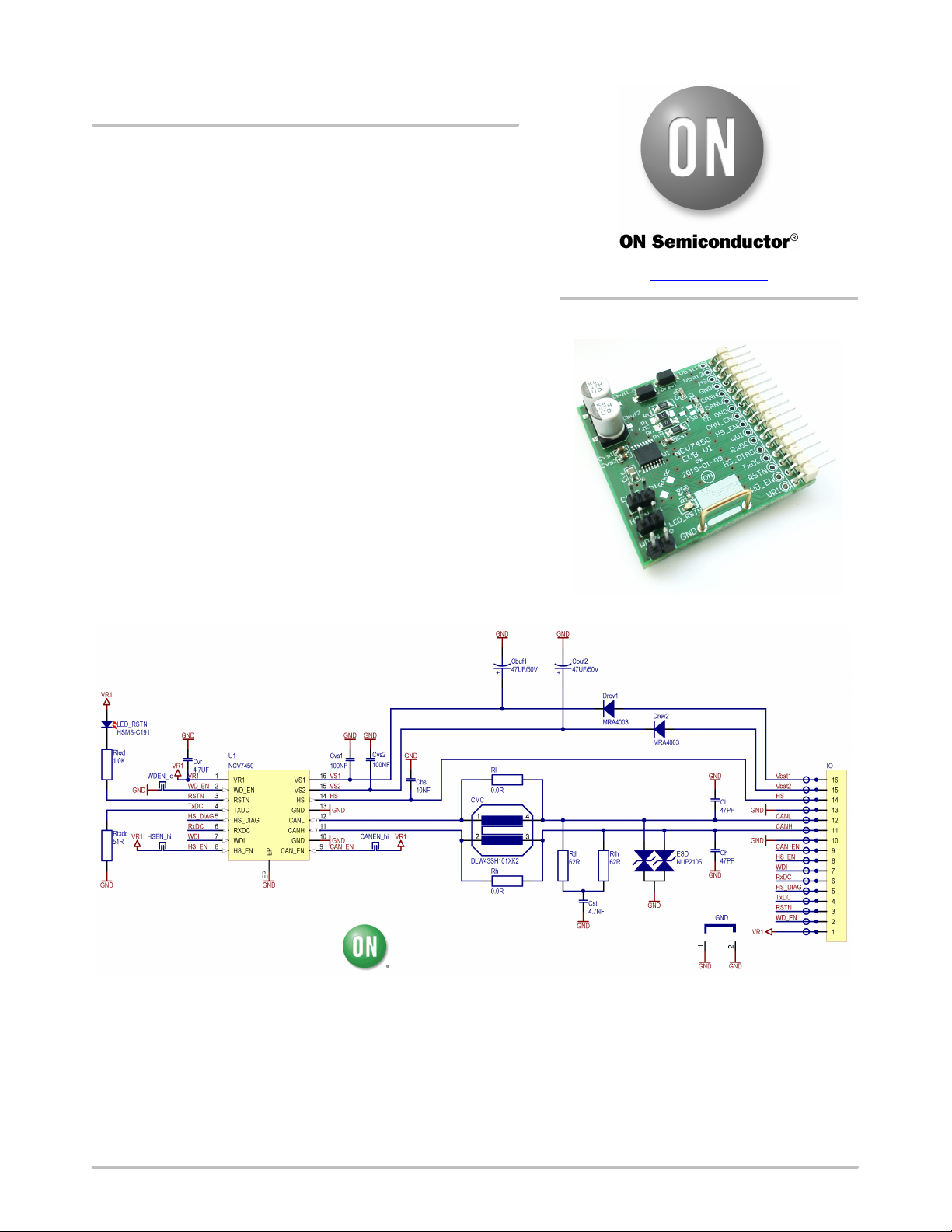
Figure 1. NCV7450V1GEVB Evaluation Board
© Semiconductor Components Industries, LLC, 2020
June, 2020 − Rev. 0
Figure 2. NCV7450 Evaluation Board Schematic
1 Publication Order Number:
EVBUM2737/D
NCV7450V1GEVB
Table 1. ABSOLUTE MAXIMUM RATINGS
Rating Pins Min Max Unit
Battery supply voltage Vbat1, Vbat2 −40 40 V
LDO Regulator output voltage VR1 −0.3 6 or VS1 + 0.5 V
Digital inputs/outputs voltage TxDC, RxDC, EN_WD, EN_CAN,
EN_HS, HS_DIAG, WDI, RSTN
CAN bus line voltage CANH, CANL −40 40 V
HS Driver output voltage HS
− with Cbuf2
− without Cbuf2
NCV7450 junction temperature −40 +150
Board temperature −40 +125
Stresses exceeding those listed in the Maximum Ratings table may damage the device. If any of these limits are exceeded, device functionality
should not be assumed, damage may occur and reliability may be affected.
−0.3 VR1 + 0.3 V V
−0.3
−0.3
(whichever is lower)
Vbat2
40
Table 2. RECOMMENDED BOARD OPERATING CONDITIONS
Rating Pins Min Max Unit
Battery supply voltage Vbat1, Vbat2 6 18 V
LDO Regulator output current
(thermally limited)
Digital inputs/outputs voltage TxDC, RxDC, EN_WD, EN_CAN,
EN_HS, HS_DIAG, WDI, RSTN
CAN bus line voltage CANH, CANL 0 5 V
HS Driver output voltage HS 0 VS2 V
HS Driver output current HS 0 1.7 A
NCV7450 junction temperature −40 +150
Board temperature −40 +125
Functional operation above the stresses listed in the Recommended Operating Ranges is not implied. Extended exposure to stresses beyond
the Recommended Operating Ranges limits may affect device reliability.
VR1 −0.1 250 mA
0 5 V
V
V
V
°C
°C
°C
°C
www.onsemi.com
2

NCV7450V1GEVB
OPERATIONAL GUIDELINES
NCV7450 evaluation board allows easy evaluation of
NCV7450 system basis chip. It provides connection to all
the device’s pins as well as positions for all the necessary
Configurations and assembly options are listed in Table 3.
For more information please check NCV7450
datasheet at www.onsemi.com
CAN bus external components.
Table 3. ASSEMBLY OPTIONS AND CONFIGURATIONS
Component Default Function
Rth, Rtl, Cst 2x 62R, 4.7nF CAN bus termination
ESD −
(optional)
Ch, Cl 47 pF ESD capacitors. Should be selected per application needs and ESD used
CMC − Optional common−mode choke
Rl, Rh 0R Bypass of CMC
Rtxdc − Not used
Cbuf2 −
(optional 47 mF)
CANEN_hi − CAN_EN pin connection
HSEN_hi − HS_EN pin connection
WDEN_lo − WD_EN pin connection
Position for optional NUP2105 ESD protection
HS driver supply buffer capacitor for, optional
w Should be used for HS driver PWM operation
w Should not be used if short to voltage higher than Vbat2 can occur
Open = CAN_EN weak internal pull−down = CAN transceiver disabled
Closed = CAN_EN connected to VR1 = CAN transceiver enabled
Open = HSN_EN weak internal pull−down = HS driver disabled
Closed = HSN_EN connected to VR1 = HS driver enabled
Open = WD_EN weak internal pull−up current source (periodically activated) =
watchdog enabled
Closed = WD_EN shorted to GND = watchdog disabled
transceiver
.
Figure 3. NCV7450 Evaluation Board Picture, Top Side
www.onsemi.com
3

Composite Drawings
NCV7450V1GEVB
PCB DRAWINGS
Figure 4. NCV7450 EVB PCB Top Drawing Figure 5. NCV7450 EVB PCB Bottom Drawing
(Bottom View)
www.onsemi.com
4

ON Semiconductor and the ON Semiconductor logo are trademarks of Semiconductor Components Industries, LLC dba ON Semiconductor or its subsidiaries in the United States and/or
other countries. ON Semiconductor owns the rights to a number of patents, trademarks, copyrights, trade secrets, and other intellectual property. A listing of ON Semiconductor’s
product/patent coverage may be accessed at www.onsemi.com/site/pdf/Patent−Marking.pdf
subject to all applicable copyright laws and is not for resale in any manner.
The evaluation board/kit (research and development board/kit) (hereinafter the “board”) is not a finished product and is as such not available for sale to consumers. The board is only intended
for research, development, demonstration and evaluation purposes and should as such only be used in laboratory/development areas by persons with an engineering/technical training
and familiar with the risks associated with handling electrical/mechanical components, systems and subsystems. This person assumes full responsibility/liability for proper and safe handling.
Any other use, resale or redistribution for any other purpose is strictly prohibited.
The board is delivered “AS IS” and without warranty of any kind including, but not limited to, that the board is production−worthy, that the functions contained in the board will meet your
requirements, or that the operation of the board will be uninterrupted or error free. ON Semiconductor expressly disclaims all warranties, express, implied or otherwise, including without
limitation, warranties of fitness for a particular purpose and non−infringement of intellectual property rights.
ON Semiconductor reserves the right to make changes without further notice to any board.
You are responsible for determining whether the board will be suitable for your intended use or application or will achieve your intended results. Prior to using or distributing any systems
that have been evaluated, designed or tested using the board, you agree to test and validate your design to confirm the functionality for your application. Any technical, applications or design
information or advice, quality characterization, reliability data or other services provided by ON Semiconductor shall not constitute any representation or warranty by ON Semiconductor,
and no additional obligations or liabilities shall arise from ON Semiconductor having provided such information or services.
The boards are not designed, intended, or authorized for use in life support systems, or any FDA Class 3 medical devices or medical devices with a similar or equivalent classification in
a foreign jurisdiction, or any devices intended for implantation in the human body. Should you purchase or use the board for any such unintended or unauthorized application, you shall
indemnify and hold ON Semiconductor and its officers, employees, subsidiaries, affiliates, and distributors harmless against all claims, costs, damages, and expenses, and reasonable
attorney fees arising out of, directly or indirectly, any claim of personal injury or death associated with such unintended or unauthorized use, even if such claim alleges that ON Semiconductor
was negligent regarding the design or manufacture of the board.
This evaluation board/kit does not fall within the scope of the European Union directives regarding electromagnetic compatibility, restricted substances (RoHS), recycling (WEEE), FCC,
CE or UL, and may not meet the technical requirements of these or other related directives.
FCC WARNING – This evaluation board/kit is intended for use for engineering development, demonstration, or evaluation purposes only and is not considered by ON Semiconductor to
be a finished end product fit for general consumer use. It may generate, use, or radiate radio frequency energy and has not been tested for compliance with the limits of computing devices
pursuant to part 15 of FCC rules, which are designed to provide reasonable protection against radio frequency interference. Operation of this equipment may cause interference with radio
communications, in which case the user shall be responsible, at its expense, to take whatever measures may be required to correct this interference.
ON Semiconductor does not convey any license under its patent rights nor the rights of others.
LIMITATIONS OF LIABILITY: ON Semiconductor shall not be liable for any special, consequential, incidental, indirect or punitive damages, including, but not limited to the costs of
requalification, delay, loss of profits or goodwill, arising out of or in connection with the board, even if ON Semiconductor is advised of the possibility of such damages. In no event shall
ON Semiconductor’s aggregate liability from any obligation arising out of or in connection with the board, under any theory of liability, exceed the purchase price paid for the board, if any.
For more information and documentation, please visit www.onsemi.com
.
. ON Semiconductor is an Equal Opportunity/Affirmative Action Employer. This literature is
PUBLICATION ORDERING INFORMATION
LITERATURE FULFILLMENT:
Email Requests to: orderlit@onsemi.com
ON Semiconductor Website: www.onsemi.com
TECHNICAL SUPPORT
North American Technical Support:
Voice Mail: 1 800−282−9855 Toll Free USA/Canada
Phone: 011 421 33 790 2910
Europe, Middle East and Africa Technical Support:
Phone: 00421 33 790 2910
For additional information, please contact your local Sales Representative
◊
www.onsemi.com
1
 Loading...