

查询NCV7380供应商
NCV7380
Advance Information
LIN Transceiver
The NCV7380 is a physical layer device for a single wire data link
capable of operating in applications where high data rate is not
required and a lower data rate can achieve cost reductions in both the
physical media components and in the microprocessor which uses
the network. The NCV7380 is designed to work in systems
developed for LIN 1.3 or LIN 2.0. The IC furthermore can be used in
ISO9141 systems.
Because of the very low current consumption of the NCV7380 in
recessive state, it’s suitable for ECU applications with low standby
current requirements, whereby no sleep/wake−up control from the
microprocessor is necessary.
Features
• Operating Voltage V
• Low Current Consumption of Typ. 24 A
• LIN−Bus Transceiver:
♦ Slew Rate Control for Good EMC Behavior
♦ Fully Integrated Receiver Filter
♦ BUS Input Voltage −27 V to 40 V
♦ Integrated Termination Resistor for LIN Slave Nodes (30 k)
♦ Baud Rate up to 20 kBaud
♦ Will Work in Systems Designed for either LIN 1.3 or LIN 2.0
• Compatible to ISO9141 Functions
• High EMI Immunity
• Bus Terminals Protect Against Short−Circuits and Transients in the
Automotive Environment
• Bus Pin High Impedance During Loss of Ground and Undervoltage
Conditions
• Thermal Overload Protection
• High Signal Symmetry for use in RC–Based Slave Nodes up to 2%
Clock Tolerance when Compared to the Master Node
• 4.0 kV ESD Protection on all Pins
• NCV Prefix for Automotive and Other Applications Requiring Site
and Change Control
= 6.0 to 18 V
S
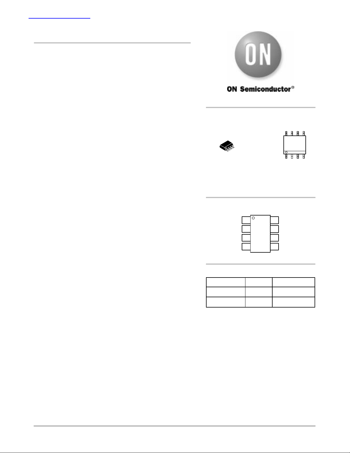
http://onsemi.com
MARKING
DIAGRAM
8
8
1
RxD
NC
VCC
TxD
ORDERING INFORMATION
Device Package Shipping†
NCV7380D SO−8 95 Units/Rail
NCV7380DR2 SO−8 2500 Tape & Reel
†For information on tape and reel specifications,
including part orientation and tape sizes, please
refer to our Tape and Reel Packaging Specifications
Brochure, BRD8011/D.
SO−8
D SUFFIX
CASE 751
A = Assembly Location
L = Wafer Lot
Y = Year
W = Work Week
PIN CONNECTIONS
18
2
3
4
(Top View)
V7380
ALYW
1
NC
7
VS
BUS
6
GND
5
This document contains information on a new product. Specifications and information
herein are subject to change without notice.
Semiconductor Components Industries, LLC, 2004
May, 2004 − Rev. P3
1 Publication Order Number:
NCV7380/D
NCV7380
NCV7380
VS
VCC
TxD
RxD
Internal Supply
and
References
POR
15 K
Biasing &
Bandgap
SLEW RATE
CONTROL
Receive
Comparator
Thermal
Shutdown
30 K
BUS Driver
BUS
GND
Input
Filter
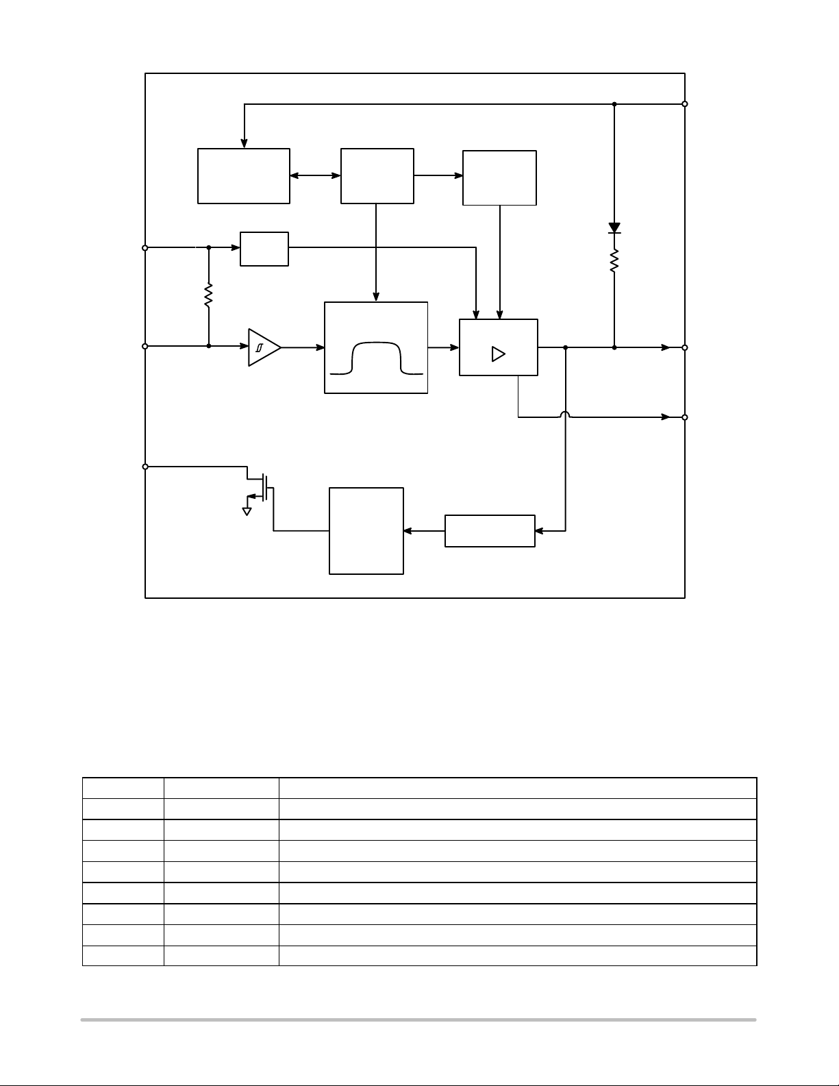
Figure 1. Block Diagram
P ACKAGE PIN DESCRIPTION
Pin Symbol Description
1 RXD Receive data from BUS to microprocessor, LOW in dominant state.
2 NC No connection.
3 VCC 5.0 V supply input.
4 TXD Transmit data from microprocessor to BUS, LOW in dominant state.
5 GND Ground
6 BUS LIN bus pin, LOW in dominant state.
7 VS Battery input voltage.
8 NC No connection.
http://onsemi.com
2
NCV7380
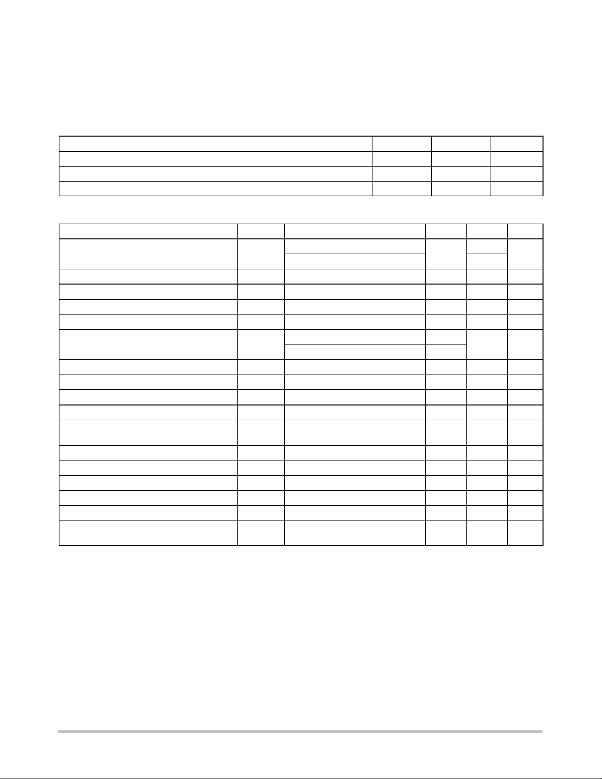
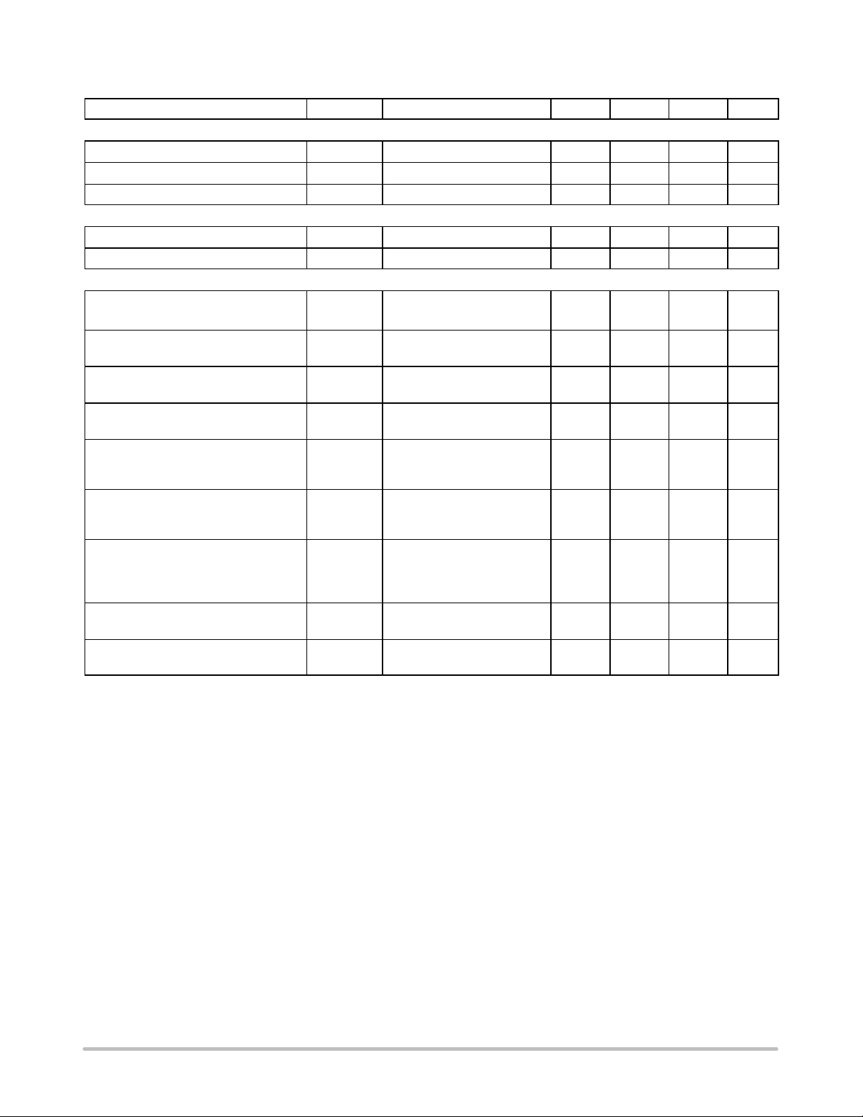
Electrical Specification
All voltages are referenced to ground (GND). Positive
currents flow into the IC.
The maximum ratings given in the table below are
limiting values that do not lead to a permanent damage of
OPERATING CONDITIONS
Characteristic Symbol Min Max Unit
Battery Supply Voltage (Note 1) V
Supply Voltage V
Operating Ambient Temperature T
MAXIMUM RATINGS
Rating Symbol Condition Min Max Unit
Battery Supply Voltage V
Supply Voltage V
Transient Supply Voltage V
Transient Supply Voltage V
Transient Supply Voltage V
BUS Voltage V
Transient Bus Voltage V
Transient Bus Voltage V
Transient Bus Voltage V
DC Voltage on Pins TxD, RxD V
ESD Capability of Any Pin V
Maximum Latch−Up Free Current at Any Pin I
Maximum Power Dissipation P
Thermal Impedance
Storage Temperature T
Junction Temperature T
Lead Temperature Soldering
Reflow: (SMD styles only)
1. VS is the IC supply voltage including voltage drop of reverse battery protection diode, V
18 V .
2. ISO 7637 test pulses are applied to VS via a reverse polarity diode and > 2.0 F blocking capacitor.
3. ISO 7637 test pulses are applied to BUS via a coupling capacitance of 1.0 nF.
S
CC
S.tr1
S..tr2
S..tr3
BUS
BUS..tr1
BUS.tr2
BUS.tr3
DC
ESDHB
LATCH
tot
JA
stg
J
T
sld
the device but exceeding any of these limits may do so.
Long term exposure to limiting values may effect the
reliability of the device.
S
CC
A
t < 1 min
Load Dump, t < 500 ms
− −0.3 +7.0 V
ISO 7637/1 Pulse 1 (Note 2) −150 − V
ISO 7637/1 Pulses 2 (Note 2) − 100 V
ISO 7637/1 Pulses 3A, 3B −150 150 V
t < 500 ms , Vs = 18 V −27
t < 500 ms ,Vs = 0 V −40
ISO 7637/1 Pulse 1 (Note 3) −150 − V
ISO 7637/1 Pulses 2 (Note 3) − 100 V
ISO 7637/1 Pulses 3A, 3B (Note 3) −150 150 V
− −0.3 7.0 V
Human body model, equivalent to
discharge 100 pF with 1.5 k
− −500 500 mA
At TA = 125°C − 197 mW
In Free Air − 152 °C/W
− −55 +150 °C
− −40 +150 °C
60 second maximum above 183°C
−5°C/+0°C allowable conditions
DROP
6.0 18 V
4.5 5.5 V
−40 +125 °C
= 0.4 to 1.0 V , V
−0.3
40
40
−4.0 4.0 kV
− 240 peak °C
voltage range is 7.0 to
BAT_ECU
30 V
V
http://onsemi.com
3
NCV7380
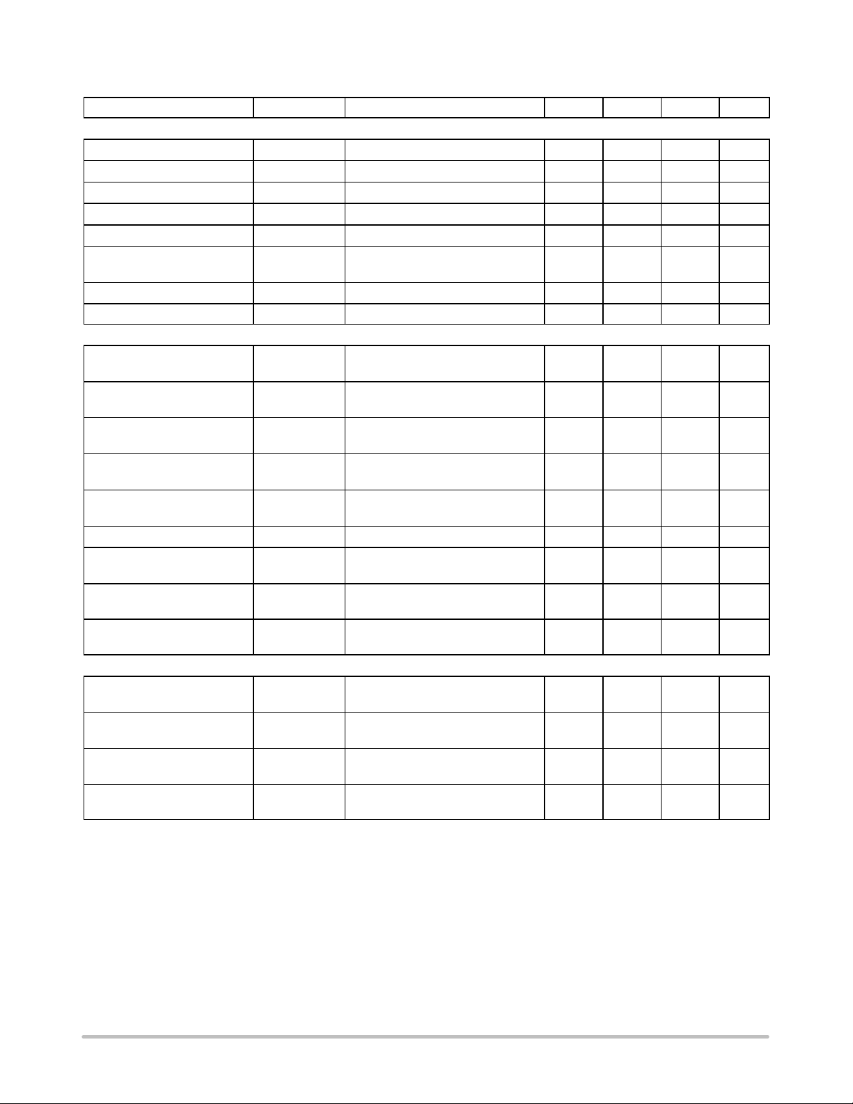
ELECTRICAL CHARACTERISTICS (V
= 6.0 to 18 V , V
S
= 4.5 to 5.5 V and T
CC
= −40 to 125°C unless otherwise noted.)
A
Characteristic Symbol Condition Min Typ Max Unit
GENERAL
V
Undervoltage Lockout V
CC
Supply Current, Dominant I
Supply Current, Dominant I
Supply Current, Recessive I
Supply Current, Recessive I
Supply Current, Recessive I
Sr +
CC_UV
Sd
CCd
Sr
CCr
I
CCr
VS > 6.0 V, TxD = L, EN = H 2.75 − 4.3 V
VS = 18 V , VCC = 5.5 V , TxD = L − 1.0 3.0 mA
VS = 18 V , VCC = 5.5 V , TxD = L − 0.8 1.5 mA
VS = 18 V , VCC = 5.5 V , TxD = Open − 10 20 A
V
= 18 V , VCC = 5.5 V , TxD = Open − 14 30 A
S
V
= 12 V , VCC = 5.0 V , TxD = Open,
S
T
= 25°
A
− 24 − A
Thermal Shutdown Tsd (Note 4) − 155 − 180 °C
Thermal Recovery T
(Note 4) − 126 140 150 °C
hys
BUS − Transmit
Short Circuit Bus Current I
BUS_LIM
V
= VS, Driver On − 120 200 mA
BUS
(Notes 5 and 6)
Pull Up Current Bus I
BUS_PU
V
BUS
= 0, V
= 12 V, Driver Off −600 − −200 A
S
(Notes 5 and 6)
Bus Reverse Current,
Recessive
Bus Reverse Current Loss of
Battery
Bus Current During Loss of
Ground
Transmitter Dominant V oltage V
Transmitter Dominant V oltage V
I
BUS_PAS_rec
(Notes 5 and 6)
I
BUS_LOG
(Notes 5 and 6)
I
BUS_LOG
(Notes 5 and 6)
BUSdom_DRV_1
BUSdom_DRV_2
V
> VS, 6.0 V < V
BUS
Driver Off
V
= 0 V , 0 V < V
S
V
= 12 V , 0 < V
S
BUS
Load = 40 mA − − 1.2 V
V
= 6.0 V , Load = 500 − − 1.2 V
S
< 18 V ,
BUS
< 18 V − − 5.0 A
BUS
< 18 V −1.0 − 1.0 mA
− − 5.0 A
(Note 5)
Transmitter Dominant V oltage V
BUSdom_DRV_3
V
= 18 V , Load = 500 − − 2.0 V
S
(Note 5)
Bus Input Capacitance C
(Note 4) Pulse Response via 10 k
BUS
V
= 12 V , VS = Open
PULSE
− 25 35 pF
BUS − Receive
Receiver Dominant Voltage V
ilBUS
− 0.4 *V
S
− − V
(Notes 5 and 6)
Receiver Recessive Voltage V
ihBUS
− − − 0.6 *V
S
(Notes 5 and 6)
Center Point of Receiver
Threshold
(Notes 5 and 6)
Receiver Hysteresis V
V
BUS_CNT
iBUS_HYS
V
BUS_CNT
V
BUS_CNTt
= (V
= (V
ilBUS
ihBUS
and V
− V
)/2 0.487
ihBUS
) − 0.16 *V
ilBUS
*V
S
0.5 *V
0.512
S
*V
S
− V
S
(Notes 5 and 6)
4. No production test, guaranteed by design and qualification.
5. In accordance to LIN physical layer specification 1.3.
6. In accordance to LIN physical layer specification 2.0.
V
V
http://onsemi.com
4
NCV7380
ELECTRICAL CHARACTERISTICS (continued) (V
= 6.0 to 18 V, V
S
= 4.5 to 5.5 V and T
CC
= −40 to 125°C unless otherwise noted.)
A
Characteristic Symbol Condition Min Typ Max Unit
TXD
High Level Input Voltage V
Low Level Input Voltage V
TxD Pull Up Resistor R
IH_TXD
ih
il
Rising Edge − − 0.7*V
Falling Edge 0.3*V
V
= 0 V 10 15 20 k
TxD
CC
− − V
CC
RXD
Low Level Output Voltage V
Leakage Current V
ol_rxd
leak_rxd
I
= 2.0 mA − − 0.9 V
RxD
V
= 5.5 V, Recessive −1.0 − 1.0 A
RxD
AC CHARACTERISTICS
Propagation Delay Transmitter
(Notes 9 and 11)
Propagation Delay Transmitter Symmetry
t
trans_pdf
t
trans_pdr
t
trans_sym
Bus Loads: 1.0 K/1.0 nF,
660 /6.8 nF, 500 /10 nF
Calculate t
trans_pdf
− t
trans_pdr
− − 5.0 s
−2.0 − 2.0 s
(Notes 7 and 11)
Propagation Delay Receiver
(Notes 7, 8, 9, 1 1 and 14)
Propagation Delay Receiver Symmetry
t
rec_pdf
t
rec_pdr
t
rec_sym
C
= 20 pF − − 6.0 s
RxD
Calculate t
trans_pdf
− t
trans_pdr
−1.5 − 1.5 s
(Notes 7 and 8)
Slew Rate Rising and Falling Edge,
High Battery (Notes 7 and 12)
t
SR_HB
Bus Loads: VS = 18 V ,
1.0 K/1.0 nF, 660 /6.8 nF,
1.0 2.0 3.0 V/s
500 /10 nF
Slew Rate Rising and Falling Edge,
Low Battery (Notes 7 and 12)
t
SR_LB
Bus Loads: VS = 7.0 V ,
1.0 K/1.0 nF, 660 /6.8 nF,
0.5 2.0 3.0 V/s
500 /10 nF
Slope Symmetry, High Battery
(Notes 7 and 12)
t
ssym_HB
Bus Loads: VS = 18 V ,
1.0 K/1.0 nF, 660 /6.8 nF,
−5.0 − 5.0 s
500 /10 nF, Calculate
t
sdom−tsrec
Bus Duty Cycle (Notes 8 and 15) D1
D2
Receiver Debounce Time
t
rec_deb
Calculate t
Calculate t
BUS_rec(min)
BUS_rec(max)
/100 s
/100 s
0.396
−
−
−
−
0.581
BUS Rising and Falling Edge 1.5 − 4.0 s
(Notes 10, 13 and 14)
7. In accordance to LIN physical layer specification 1.3.
8. In accordance to LIN physical layer specification 2.0.
9. Propagation delays are not relevant for LIN protocol transmission, only symmetry.
10.No production test, guaranteed by design and qualification.
11.See Figure 2 − Input/Output Timing.
12.See Figure 7 − Slope Time Calculation.
13.See Figure 3 − Receiver Debouncing.
14.This parameter is tested by applying a square wave to the bus. The minimum slew rate for the bus rising and falling edges is 50 V/s.
15.See Figure 8 − Duty Cycle Measurement and Calculation.
V
s/s
s/s
http://onsemi.com
5

NCV7380
TIMING DIAGRAMS
TxD
BUS
RxD
50%
t
trans_pdf
V
BUS
95%
100%
50%
t
trans_pdr
50%
5%
0%
t
rec_pdf
t
rec_pdr
50%
Figure 2. Input/Output Timing
t < t
rec_deb
t < t
rec_deb
V
BUS
60%
40%
t
V
RxD
50%
t
Figure 3. Receiver Debouncing Filter
http://onsemi.com
6

NCV7380
TEST CIRCUITS FOR DYNAMIC AND STATIC CHARACTERISTICS
NCV7380
VSUP
R
C
100 nF
L
BUS
L
GND
VCC
TxD
RxD
Figure 4. Test Circuit for Dynamic Characteristics
NCV7380
500
2 F
VSUP
+
VCC
100 nF
2.7 K
20 pF
100 nF
BUS
1 nF
GND
Schaffner−
Generator
Puls3a,3b
Puls1,2,4
TxD
RxD
Figure 5. Test Circuit for Automotive Transients
12 V
Oscilloscope
+
−
http://onsemi.com
7

NCV7380
Functional Description
Initialization
After power on, the chip automatically enters the
recessive state (TxD = Open). Both VCC and VS must be
present.
Operating Modes
All operation modes will be handled from the NCV7380
automatically.
Normal Mode
After power on, the IC switches automatically to normal
mode. Bus communication is possible. If there is no
communication on the bus line the power consumption of
the IC is very low and does not require microprocessor
control.
Thermal Shutdown Mode
If the junction temperature TJ is higher than 155°C, the
NCV7380 could be switched into the thermal shutdown
mode (bus driver will be switched off, receiver is on).
If TJ falls below the thermal shutdown temperature (typ.
140°C) the NCV7380 will be switched to the normal mode.
LIN BUS Transceiver
The transceiver consists of a bus−driver (1.2 V @
40 mA) with slew rate control and current limit, and a
receiver with a high voltage comparator with filter
circuitry.
BUS Input/Output
The recessive BUS level is generated from the integrated
30 k pull up resistor in series with a diode. The diode
prevents reverse current on V
BUS
when V
BUS
> V
.
S
No additional termination resistor is necessary to use the
NCV7380 on LIN slave nodes. If this IC is used for LIN
master nodes, it is necessary to terminate the bus with an
external 1.0 k resistor in series with a diode to VBAT
(Figure 9).
TxD Input
During transmission the signal on TxD will be
transferred to the BUS driver for generating a BUS signal.
To minimize the electromagnetic emission of the bus line,
the BUS driver has integrated slew rate control and wave
shaping.
Transmitting will be interrupted if thermal shutdown is
active.
The CMOS compatible input TxD directly controls the
BUS level:
TxD = low → BUS = low (dominant level)
TxD = high → BUS = high (recessive level)
The TxD pin has an internal pull up resistor connected to
VCC. This secures that an open TxD pin generates a
recessive BUS level.
RxD Output
The signal on the BUS pin will be transferred
continuously to the RxD pin. Short spikes on the bus signal
are filtered with internal circuitry (Figure 3 and Figure 6).
BUS
RxD
VS
60%
50%
40%
V
BUS_CNT_max
V
BUS_CNT_min
V
hHYS
t < t
rec_deb
Figure 6. Receive Impulse Diagram
t < t
rec_deb
http://onsemi.com
8

NCV7380
The receive threshold values V
V
BUS_CNT_min
of 0.16*V
are symmetrical to 0.5*VS with a hysteresis
(typ). The LIN specific receive threshold is
S
BUS_CNT_max
and
between 0.4*VS and 0.6*VS.
The received BUS signal will be output to the RxD pin:
BUS < V
BUS_CNT
– 0.5 * V
HYS
→ RxD = low (BUS dominant)
BUS > V
BUS_CNT
+ 0.5 * V
HYS
→ RxD = high, floating (BUS recessive)
RxD is a buffered open drain output with a typical load
of:
Resistance: 2.7 k
Capacitance: < 20 pF
Data Rate
The NCV7380 is a constant slew rate transceiver. The
bus driver operates with a fixed slew rate range of 1.0 V/s
V/T 3.0 V/s. This principle provides very good
symmetry of the slope times between recessive to dominant
and dominant to recessive slopes within the LIN bus load
range (C
BUS
, R
term
).
The NCV7380 guarantees data rates up to 20 kbit within
the complete bus load range under worst case conditions.
The constant slew rate principle holds appropriate voltage
levels and can operate within the LIN Protocol
Specification for RC oscillator systems with a matching
tolerance up to 2%.
Operating Under Disturbance
Loss of Battery
If VS and VCC are disconnected from the battery, the bus
pin is in high impedance state. There is no impact to the bus
traffic.
Loss of Ground
In case of an interrupted ground connection from VS and
VCC, there is no influence to the bus line.
Short Circuit BUS to Battery
The transmitter output current is limited to 200 mA
(max) in case of short circuit to battery.
Short Circuit BUS to Ground
Negative voltages on the bus pin are limited to current
through the internal 30 k resistor and series diode from VS.
Thermal Overload
The NCV7380 is protected against thermal overloads. If
the chip temperature exceeds the thermal shutdown
threshold, the transmitter is switched off until thermal
recovery. The receiver continues to work during thermal
shutdown.
Undervoltage V
CC
The VCC undervoltage lockout feature disables the
transmitter until it is above the undervoltage lockout
threshold to prevent undesirable bus traffic.
Application Hints
LIN System Parameter
Bus Loading Requirements
Parameter Symbol Min Typ Max Unit
Operating Voltage Range V
Voltage Drop of Reverse Protection Diode V
Voltage Drop of Bus Decouple Diode in the Master Node V
Battery Offset Voltage V
Ground Offset Voltage V
Master Termination Resistor R
Slave Termination Resistor R
Number of System Nodes N 2 − 16 −
Network Distance between any two ECU Nodes B
Line Capacitance C
Capacitance of Master Node C
Capacitance of Slave Node C
Network Total Capacitance C
Network Total Resistance R
Time Constant of Overall System τnet 1.0 − 5.0 s
BAT
Drop_rev
Drop_dec
batoff
goff
pu_master
pu_slave
US_length
LINE
Master
Slave
t1
t1
8.0 − 18 V
0.4 − 1.0 V
0.4 − 1.0 V
− − 0.1 V
− − 0.1 V
900 1000 1100
20 30 60 k
− − 40 m
− 100 150 pF/m
− 220 − pF
195 220 300 pF
1.0 4.0 10 nF
537 − 863
BAT
BAT
http://onsemi.com
9

NCV7380
Recommendations for System Design
The goal of the LIN physical layer standard is to have a
universal definition of the LIN system for plug and play
solutions in LIN networks up to 20 kbd bus speeds.
In case of small and medium LIN networks, it’s
recommended to adjust the total network capacitance to at
least 4.0 nF for good EMC and EMI behavior. This can be
done by setting only the master node capacitance. The
slave node capacitance should have a unit load of typically
220 pF for good EMC/EMI behavior.
In large networks with long bus lines and the maximum
number of nodes, some system parameters can exceed the
defined limits and the LIN system designer must intervene.
The whole capacitance of a slave node is not only the unit
load capacitor itself. Additionally, there is the capacitance
of wires and connectors, and the internal capacitance of the
LIN transmitter. This internal capacitance is strongly
dependent on the technology of the IC manufacturer and
should be in the range of 30 pF to 150 pF. If the bus lines
have a total length of nearly 40m, the total bus capacitance
can exceed the LIN system limit of 10 nF.
A second parameter of concern is the integrated slave
termination resistor tolerance. If most of the slave nodes
have a slave termination resistance at the allowed
maximum of 60 k, the total network resistance is more
than 700 . Even if the total network capacitance is below
or equal to the maximum specified value of 10 nF, the
network time constant is higher than 7.0 s.
This problem can be solved only by adjusting the master
termination resistor to the required maximum network time
constant of 5.0 s (max).
The LIN bus output driver of the NCV7380 provides a
higher drive capability than necessary (40 mA @ 1.2 V)
within the LIN standard (33.6 mA @ 1.2 V). With this
driver stage the system designer can increase the maximum
LIN networks with a total network capacitance of more
than 10 nF. The total network resistance can be decreased
to:
R
(V
tl_min
Bat_max
(18 V 1.2 V)40 mA 420
V
BUSdom
)I
BUS_max
NOTE: The NCV7380 meets the requirements for
implementation in RC−based slave nodes. The LIN
Protocol Specification requires the deviation of the slave
node clock to the master node clock after synchronization
must not differ by more than 2%.
Setting the network time constant is necessary in large
networks (primarily resistance) and also in small networks
(primarily capacitance).
MIN/MAX SLOPE TIME CALCULATION
(In accordance to the LIN System Parameter Table)
V
BUS
100%
60%
40%
0%
t
sdom
Figure 7. Slope Time and Slew Rate Calculation
(In accordance to LIN physical layer specification 1.3)
The slew rate of the bus voltage is measured between
40% and 60% of the output voltage swing (linear region).
The output voltage swing is the difference between
dominant and recessive bus voltage.
dVdt 0.2 * V
swing
(t
40%−t60%
)
The slope time is the extension of the slew rate tangent
until the upper and lower voltage swing limits:
t
slope
5*(t
40%−t60%
)
60%
40%
V
dom
t
srec
The slope t ime of the recessive to d ominant e dge i s d irectly
determined by the slew rate control of the transmitter:
t
slope
V
swing
dVdt
The dominant to recessive edge is influenced from the
network time constant and the slew rate control, because it’s
a passive edge. In case of low battery volt ages and high bus
loads t he rising edge is only determined by t he network. If the
rising edge slew rate exceeds the value of the dominant one,
the slew ra t e cont rol det e rmi ne s the ri sing edge .
http://onsemi.com
10

NCV7380
TxD
V
BUS
GND
RxD
SUP
100%
0%
58.1%
28.4%
t
Bit
t
dom(max)
t
dom(min)
74.4%
42.2%
t
Bit
t
rec(min)
58.1%
t
rec(max)
28.4%
Figure 8. Duty Cycle Measurement and Calculation in Accordance to LIN Physical Layer Specification 2.0
Duty Cycle Calculation
With the timing parameters shown in Figure 8 two duty
cycles, based on t
rec(min)
and t
can be calculated as
rec(max)
follows:
D1* = t
D2* = t
rec(min)
rec(max)
/(2 x t
/(2 x t
Bit
Bit
)
)
For proper operation at 20 KBit/s (bit time is 50 s) the
LIN driver has to fulfill the duty cycles specified in the AC
characteristics for supply voltages of 7...18 V and the three
defined standard loads.
Due to this simple definition there is no need to measure
slew rates, slope times, transmitter delays and dominant
voltage levels as specified in the LIN physical layer
specification 1.3.
The devices within the D1/D2 duty cycle range also
operates in applications with reduced bus speed of
10.4 KBit/s or below.
In order to minimize EME, the slew rates of the
transmitter can be reduced (by up to 2 times). Such
devices have to fulfill the duty cycle definition D3/D4 in
the LIN physical layer specification 2.0. Devices within
this duty cycle range cannot operate in higher frequency
20 KBit/s applications.
*D1 and D2 are defined in the LIN protocol specification 2.0.
http://onsemi.com
11

NCV7380
Ignition
Car Battery
1N4001
V
BAT
10 F
100 nF
V
OUT
V
Voltage
Regulator
NCV8502
10 k
P
GND
LIN BUS
2.2 F
IN
100 nF
Reset
47 nF
2.7 K
VCC VS
RxD
TxD
BUS
NCV7380
GND
Slave
ECU
220 pF
LIN Bus
to Single Wire
ECU Connector
*
BUS
2.2 F
100 nF
47 nF
220 pF
Master
ECU
1 K
LIN Bus
to Single Wire
ECU Connector
1N4001
V
BAT
V
OUT
10 F
100 nF
V
Voltage
Regulator
NCV8501
10 k
P
GND
IN
2.7 K
10 k
VCC VS
INH
RxD
NCV7382
TxD
EN
GND
ENABLE
Reset
47 nF
*The NCV7382 is a pin compatible transceiver with INH control.
Figure 9. Application Circuitry
http://onsemi.com
12

NCV7380
ESD/EMC Remarks
General Remarks
Electronic semiconductor products are sensitive to
Electro Static Discharge (ESD). Always observe Electro
Static Discharge control procedures whenever handling
semiconductor products.
POWER SUPPLY PIN VS
Test Pulse Condition Duration
1 t1 = 5.0 s/US = −100 V/tD = 2.0 ms 5000 Pulses
2 t1 = 0.5 s/US = 100 V/tD = 0.05 ms 5000 Pulses
3a/b US = −150 V/US = 100 V
Burst 100 ns/10 ms/90 ms Break
5 Ri = 0.5 , tD = 400 ms
tr = 0.1 ms/UP + US = 40 V
DATA AND SIGNAL PINS BUS
Test Pulse Condition Duration
1 t1 = 5.0 s/US = −100 V/tD = 2.0 ms 1000 Pulses
2 t1 = 0.5 s/US = 100 V/tD = 0.05 ms 1000 Pulses
3a/b US = −150 V/US = 100 V
Burst 100 ns/10 ms/90 ms Break
ESD Test
The NCV7380 is tested according to MIL883D (human
body model).
EMC
The test on EMC impacts is done according to ISO
7637−1 for power supply pins and ISO 7637−3 for data and
signal pins.
1 h
10 Pulses Every 1 Min
1000 Burst
http://onsemi.com
13

−Y−
−Z−
NCV7380
PACKAGE DIMENSIONS
SO−8
CASE 751−07
ISSUE AB
−X−
B
H
A
58
1
4
G
D
0.25 (0.010) Z
M
S
Y
0.25 (0.010)
C
SEATING
PLANE
SXS
M
0.10 (0.004)
M
Y
K
N
X 45
M
J
NOTES:
1. DIMENSIONING AND TOLERANCING PER
ANSI Y14.5M, 1982.
2. CONTROLLING DIMENSION: MILLIMETER.
3. DIMENSION A AND B DO NOT INCLUDE
MOLD PROTRUSION.
4. MAXIMUM MOLD PROTRUSION 0.15 (0.006)
PER SIDE.
5. DIMENSION D DOES NOT INCLUDE DAMBAR
PROTRUSION. ALLOWABLE DAMBAR
PROTRUSION SHALL BE 0.127 (0.005) TOTAL
IN EXCESS OF THE D DIMENSION AT
MAXIMUM MATERIAL CONDITION.
6. 751−01 THRU 751−06 ARE OBSOLETE. NEW
STANDARD IS 751−07.
MILLIMETERS
DIMAMIN MAX MIN MAX
4.80 5.00 0.189 0.197
B 3.80 4.00 0.150 0.157
C 1.35 1.75 0.053 0.069
D 0.33 0.51 0.013 0.020
G 1.27 BSC 0.050 BSC
H 0.10 0.25 0.004 0.010
J 0.19 0.25 0.007 0.010
K 0.40 1.27 0.016 0.050
M 0 8 0 8
N 0.25 0.50 0.010 0.020
S 5.80 6.20 0.228 0.244
INCHES
SOLDERING FOOTPRINT*
1.52
0.060
7.0
0.275
0.6
0.024
*For additional information on our Pb−Free strategy and soldering
details, please download the ON Semiconductor Soldering and
Mounting Techniques Reference Manual, SOLDERRM/D.
ON Semiconductor and are registered trademarks of Semiconductor Components Industries, LLC (SCILLC). SCILLC reserves the right to make changes without further notice
to any products herein. SCILLC makes no warranty, representation or guarantee regarding the suitability of its products for any particular purpose, nor does SCILLC assume any
liability arising out of the application or use of any product or circuit, and specifically disclaims any and all liability, including without limitation special, consequential or incidental
damages. “Typical” parameters which may be provided in SCILLC data sheets and/or specifications can and do vary in different applications and actual performance may vary over
time. All operating parameters, including “Typicals” must be validated for each customer application by customer’s technical experts. SCILLC does not convey any license under
its patent rights nor the rights of others. SCILLC products are not designed, intended, or authorized for use as components in systems intended for surgical implant into the body,
or other applications intended to support or sustain life, or for any other application in which the failure of the SCILLC product could create a situation where personal injury or death
may occur. Should Buyer purchase or use SCILLC products for any such unintended or unauthorized application, Buyer shall indemnify and hold SCILLC and its officers, employees,
subsidiaries, affiliates, and distributors harmless against all claims, costs, damages, and expenses, and reasonable attorney fees arising out of, directly or indirectly, any claim of
personal injury or death associated with such unintended or unauthorized use, even if such claim alleges that SCILLC was negligent regarding the design or manufacture of the part.
SCILLC is an Equal Opportunity/Affirmative Action Employer. This literature is subject to all applicable copyright laws and is not for resale in any manner.
4.0
0.155
1.270
0.050
SCALE 6:1
inches
mm
PUBLICATION ORDERING INFORMATION
LITERATURE FULFILLMENT:
Literature Distribution Center for ON Semiconductor
P.O. Box 5163, Denver, Colorado 80217 USA
Phone: 303−675−2175 or 800−344−3860 Toll Free USA/Canada
Fax: 303−675−2176 or 800−344−3867 Toll Free USA/Canada
Email: orderlit@onsemi.com
N. American Technical Support: 800−282−9855 Toll Free
USA/Canada
Japan: ON Semiconductor, Japan Customer Focus Center
2−9−1 Kamimeguro, Meguro−ku, Tokyo, Japan 153−0051
Phone: 81−3−5773−3850
http://onsemi.com
14
ON Semiconductor Website: http://onsemi.com
Order Literature: http://www.onsemi.com/litorder
For additional information, please contact your
local Sales Representative.
NCV7380/D
 Loading...