

查询NCV7361供应商
NCV7361A
Advance Information
Voltage Regulator with
Integrated LIN Transceiver
The NCV7361A consists of a low drop voltage regulator,
5.0 V/50 mA and a LIN bus transceiver. The LIN transceiver is
suitable for LIN bus systems compatible to
“LIN−Protocol Specification” Rev. 1.3, 2.0 and SAE J2602.
The combination of voltage regulator and bus transceiver make it
ideal for a powerful and inexpensive cost effective slave node in a
LIN Bus system.
Features
• Operating Voltage V
• Very Low Standby Current Consumption < 110 A in Normal Mode
(< 50 A in Sleep Mode)
• LIN−Bus Transceiver:
♦ PNP−Bipolar Transistor Driver
♦ Slew Rate Control and Wave Shaping for Best EMC Behavior
♦ BUS Input Voltage −24 V to 30 V (Independent of V
♦ Wake−Up Via LIN Bus
♦ Baud Rate up to 20 kBaud
♦ Compatible to LIN Specification 1.3, 2.0 and SAE J2602
♦ Compatible to ISO9141 Functions
• Wake−Up by LIN BUS and Startup Capable Independent of EN
Voltage Level
• Linear Low Drop Voltage Regulator:
♦ Output Voltage 5.0 V 2%
♦ Output Current Max. 50 mA
♦ Output Current Limit
♦ Overtemperature Shutdown
• Reset Time 100 ms and Reset Threshold Voltage 4.65 V
• CMOS Compatible Interface to Microcontroller
• Load Dump Protected (40 V Peak)
• Resistant Against Transient Pulses According to ISO 7637 at
Pin V
, BUS and EN
SUP
• NCV Prefix for Automotive and Other Applications Requiring Site
and Change Control
= 5.5 to 18 V
SUP
SUP
)
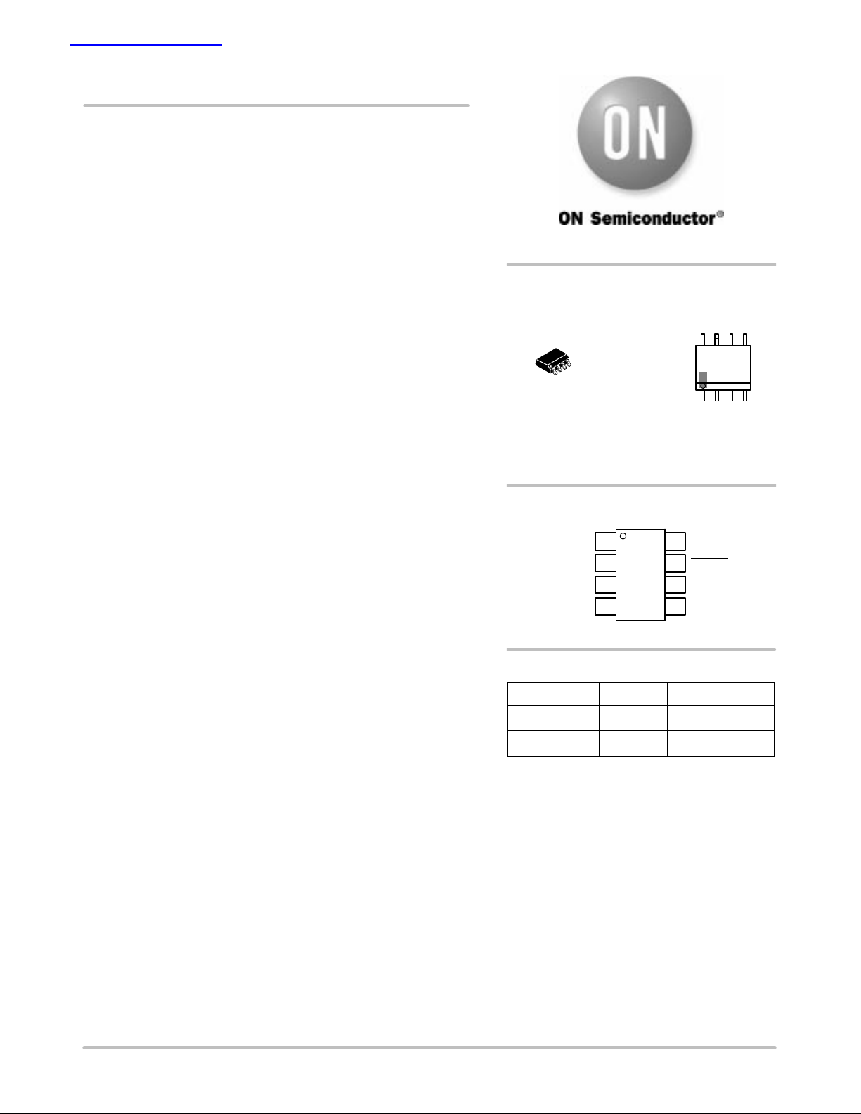
http://onsemi.com
MARKING
DIAGRAM
8
8
1
V
SUP
EN
GND
BUS
ORDERING INFORMATION
Device Package Shipping
NCV7361AD SO−8 98 Units/Rail
NCV7361ADR2 SO−8 2500 T ape & Reel
†For information on tape and reel specifications,
including part orientation and tape sizes, please
refer to our Tape and Reel Packaging Specifications
Brochure, BRD8011/D.
SO−8
D SUFFIX
CASE 751
A = Assembly Location
L = Wafer Lot
Y = Year
W = Work Week
PIN CONNECTIONS
18
2
3
4
(Top View)
7
6
5
7361A
ALYW
1
V
OUT
RESET
TxD
RxD
†
This document contains information on a new product. Specifications and information
herein are subject to change without notice.
Semiconductor Components Industries, LLC, 2004
October, 2004 − Rev. P0
1 Publication Order Number:
NCV7361A/D
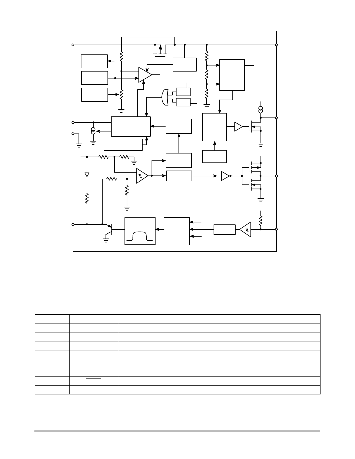
NCV7361A
V
SUP
EN
GND
BUS
Bandgap
Adjustment
V
SUP
Aux.
Supply
30 k
VBG
Mode
Control
Thermal
Protection
Slew Rate
Control
Amplifier
+
−
Receiver
Control
T
SHD
Current
Limitation
I
VAUX
POR
UVR
Wake−Up
Control
Wake−
Filter
Rec−Filter
Driver
Control
V
OUT
MR
Reset
Generator
V
SUP
4.65 V
V
OUT
RESET
Reset
Timer
V
OSC
OUT
RxD
V
OUT
T
SHD
MR
Filter
TxD
MR = Master Reset
T
= Thermal Shutdown
SHD
VBG = Bandgap V oltage
Figure 1. Block Diagram
P ACKAGE PIN DESCRIPTION
Pin Symbol Description
1 V
SUP
2 EN Enable input controls the regulator. Active high.
3 GND Ground
4 BUS LIN bus line.
5 RxD Receive output (push−pull to V
6 TxD Transmit input (pullup−input to V
7 RESET Reset output, active low (pullup to V
8 V
OUT
Supply voltage.
Regulator output 5.0 V/50 mA.
OUT
OUT
).
).
OUT
).
http://onsemi.com
2
NCV7361A
ELECTRICAL SPECIFICATIONS
All voltages are referenced to ground (GND). Positive
currents flow into the IC.
The maximum ratings (in accordance with IEC 134)
given in the table below are limiting values that do not lead
these limits may do so. Long term exposure to limiting
values may affect the reliability of the device. Correct
operating of the device can’t be guaranteed if any of these
limits are exceeded.
to a permanent damage of the device but exceeding any of
OPERATING CONDITIONS
Characteristic Symbol Min Max Unit
Supply Voltage V
Operating Ambient Temperature T
Junction Temperature T
SUP
A
J
MAXIMUM RATINGS
Rating Symbol Condition Min Max Unit
V
SUP
BUS V
Difference V
SUP−VOUT
EN V
TxD, RxD, RESET V
EN, TxD, RxD, RESET I
Short Circuit of Pin V
SUP
and V
OUT
ESD Capability TxD Pin ESD
ESD Capability on All Other Pins ESD
Junction Temperature T
Storage Temperature T
Lead Temperature Soldering
Reflow: (SMD styles only)
Maximum ratings are those values beyond which device damage can occur. Maximum ratings applied to the device are individual stress limit values
(not normal operating conditions) and are not valid simultaneously. If these limits are exceeded, device functional operation is not implied, damage
may occur and reliability may be affected.
V
SUP
BUS
V
SUP−VOUT
INEN
IN
IN
I
INSH
BUSHB
J
STG
T
sld
− −1.0 30 V
T 500 ms − 40
− −24 30 V
T 500 ms − 40
− −0.3 40 V
− −0.3 V
− −0.3 V
− −25 25 mA
− −500 500 mA
Human Body Model, 100 pF via 1.5 k −1.0 1.0 kV
Human Body Model, 100 pF via 1.5 k −2.0 2.0 kV
HB
− − 150 °C
− −55 150 °C
60 second maximum above 183°C
−5°C/+0°C allowable conditions
5.25 18 V
−40 +125 °C
− +150 °C
+
SUP
0.3
+
OUT
0.3
− 240 peak °C
V
V
THERMAL RATINGS
Parameter Test Conditions Typical Value Units
SO−8 Package Min−Pad Board (Note 1) 1.0 in Pad Board (Note 2)
Junction−to−Tab (psi−JL2,
Junction−to−Ambient (R
) (Note 3) 48 43 °C/W
JL2
, JA) 183 120 °C/W
JA
1. 1 oz copper, 54 mm2 copper area, 0.062” thick FR4.
2. 1 oz copper, 714 mm2 copper area, 0.062” thick FR4.
3. psi−JL2 temperature was made at foot of lead #2.
http://onsemi.com
3
NCV7361A
ELECTRICAL CHARACTERISTICS (5.25 V V
18 V, −40°C TA 125°C unless otherwise noted)
SUP
Characteristic Symbol Condition Min Typ Max Unit
V
SUP
Supply Current with V
“No Load’’ (Note 4)
OUT
Supply Current, “Sleep Mode’’ I
Thermal Shutdown (Note 5) T
Thermal Recovery (Note 5) T
V
Undervoltage Reset “OFF” V
SUP
V
Undervoltage Reset “ON” V
SUP
V
Undervoltage Hysteresis V
SUP
Operating Voltage V
V
OUT
Output Voltage V
Drop−Out Voltage (Note 6)
VD = V
SUP−VOUT
Output Current IV
Load Capacity C
I
Snl
Ssleep
JSHD
Jrec
SUVR_OFF
SUVR_ON
SUVR_HYS
SUP
OUTt
V
OUTh
V
OUTl
V
D
OUT
load
V
= V
EN
V
− 0.5 V , Pins 5 to 8 Open
SUP
V
= 12 V , VEN = 0 V , V
SUP
V
V
V
SUP
V
SUVR_OFF
5.5 V V
0 < I
IV
= 20 mA, V
OUT
IV
= 50 mA, V
OUT
IV
IV
3.0 V < V
Reference Figure 35 4.7 − − F
ENABLE (EN)
Input Voltage Low V
Input Voltage High V
Hysteresis (Note 5) V
Pulldown Current I
ENL
ENH
ENHYS
pdEN
RESET
Output Voltage Low V
OL
I
= 1.0 mA, V
OUT
10 k RESET to V
V
SUP
Pullup Current I
RESET Threshold V
Master Reset Threshold (Note 5) V
pu
RES
MRes
Referred to V
4. See Figure 6 for test setup.
5. Not production tested, guaranteed by design and qualification.
6. Measured when the output voltage has dropped 100 mV from the V
SUP
SUP
= 12 V , V
− 0.5 V
BUS
BUS
>
>
− − 110 A
− 35 50 A
− 155 − 175 °C
− 126 − 130 °C
Ramp Up 3.1 3.5 3.9 V
SUP
Ramp Down 2.7 3.0 3.3 V
− V
SUVR_ON
0.2 − − V
5.25 12 18 V
18 V
SUP
< 50 mA
OUT
V
> 18 V 4.90 5.0 5.25 V
SUP
= 3.3 V − V
SUP
= 3.3 V − V
SUP
= 20 mA − − 150 mV
OUT
= 50 mA − − 500 mV
OUT
< 18 V
SUP
V
= 0 V
OUT
4.90 5.0 5.10 V
SUP−VD
SUP−VD
− V
− V
50 − 150 mA
− −0.3 − 1.6 V
− 2.5 − V
SUP
+0.3
− 100 − − mV
VEN > V
VEN < V
= V
OUT
ENH
ENL
> 5.5 V − − 0.8 V
SUP
OUT
= 0.8 V
1.0 4.0 7.0 A
70 100 130 A
− − 0.2 V
− −500 −375 −250 A
, V
OUT
> 4.6 V 4.5 4.65 4.8 V
SUP
− 3.0 3.15 3.3 V
= 12 V nominal value.
SUP
V
http://onsemi.com
4
NCV7361A
ELECTRICAL CHARACTERISTICS (5.25 V V
18 V, −40°C TA 125°C unless otherwise noted)
SUP
Characteristic Symbol Condition Min Typ Max Unit
LIN BUS INTERFACE
Receive Threshold V
Receive Center Point
V
thr_cnt
= (V
thr_rec
+ V
thr_dom
)/2
Receive Hysteresis
V
thr_hys
= V
thr_rec
− V
thr_dom
BUS Input Current (Recessive)
(Note 7)
BUS Input Current (Recessive) −I
BUS Input Current (Recessive) −I
BUS Pullup Resistor R
BUS Output Voltage (Dominant)
(Note 7)
BUS Output Voltage (Recessive)
thr_rec
V
thr_dom
V
thr_cnt
V
thr_hys
I
INBUSR
INBUSR
INBUSR
BUSpu
V
BUSdom
V
BUSrec
,
V
SUP
7.0 V V
8.0 V
= V
V
SUP
V
SUP
BUS
= 0 V , V
= Open, V
18 V
SUP
18 V,
BUS
− 0.7 V, TxD = 4.5 V
= −12 V −1.0 − − mA
BUS
= −18 V −1.0 − − mA
BUS
0.4 *V
0.475
*V
SUP
0.12 *V
SUP
SUP
− 0.6
0.5
*V
SUP
0.135
*V
SUP
*V
SUP
0.525
*V
SUP
0.15
*V
SUP
− − 20 A
V
− 20 30 47 k
7.0 V
7.0 V
18 V, TxD = 0 V ,
SUP
RL = 500
18 V, TxD = 4.5 V 0.8 *V
SUP
− − 1.2 V
SUP
− − V
(Notes 7 and 8)
BUS Current Limit I
LIM
V
> 2.5 V, TxD = 0 V 40 − 120 mA
BUS
TxD
Pullup Resistance R
pu_TxD
Input Low Level V
Input High Level V
IL
IH
− 9.5 15 21 k
− − − 1.25 V
− 3.75 − − V
RxD
Output Voltage Low V
Output Voltage High V
OL
OH
I
= 1.0 mA − − 0.8 V
OUT
I
= −1.0 mA 4.2 − − V
OUT
7. See Figures 7, 8, and 9 for test setup.
8. The recessive voltage on BUS should be less than 80% direct battery. The LIN protocol requires an external reverse battery diode between
the battery and V
SUP
. V
SUP
= V
BAT
−0.7 V .
http://onsemi.com
5
NCV7361A
ELECTRICAL CHARACTERISTICS (7.0 V V
18 V, −40°C TA 125°C unless otherwise noted)
SUP
Characteristic Symbol Condition Min Typ Max Unit
RESET AC CHARACTERISTICS
Reset Time t
Reset Rise Time (Note 9) t
BUS Debounce Time (Note 14) t
Wake−Up Time t
Res
rr
deb_BUS
Wake_BUS
GENERAL LIN BUS INTERFACE AC CHARACTERISTICS
Transmit Propagation Delay
TxD −> BUS (Notes 10 and 11 )
Symmetry of Propagation Delay
BUS −> RxD (Note 10)
Receiver Propagation Delay
BUS −> RxD (Notes 10 and 11)
Symmetry of Propagation Delay
TxD −> BUS (Note 10)
Slew Rate BUS Rising Edge (Note 9) dV/dT
Slew Rate BUS Falling Edge (Note 9) dV/dT
t
dr_TxD
t
df_TxD
t
dsym_TxD
t
dr_RxD
t
df_RxD
t
dsym_RxD
,
rise
fall
LIN BUS PARAMETER ACCORDING T O LIN SPEC. REV. 1.3
Slope Time, Transition from Recessive to
Dominant (Notes 11 and 12)
Slope Time, Transition from Dominant to
Recessive (Notes 11 and 13)
Slope Time Symmetry t
Slope Time, Transition from Recessive to
Dominant (Notes 11 and 12)
Slope Time, Transition from Dominant to
Recessive (Notes 11 and 13)
Slope Time Symmetry t
t
sdom
t
srec
ssym
t
sdom
t
srec
ssym
9. Not production tested, guaranteed by design and qualification.
10.See Figures 2 and 3, Timing Diagrams.
11.See Figures 5, 6, 7, 8, and 9 for test setup.
12.t
= (t
sdom
sdom
= (t
VBUS40%
VBUS60%
13.t
14.See Figure 18.
− t
VBUS95%
− t
VBUS5%
) / 0.55.
) / 0.55.
5.25 V
5.25 V
RL/CL at BUS
1.0 k/1.0 nF
660 /6.8 nF
500 /10 nF
t
dr_TxD
C
L(RxD)
t
dr_RxD
20% V
C
= 1.0 nF, R
L
20% V
C
= 1.0 nF, R
L
V
R
= 500 /C
L
V
R
= 500 /C
L
V
R
= 500 /C
L
T
ssym
V
R
= 500 /C
L
V
R
= 500 /C
L
V
R
= 500 /C
L
T
ssym
18 V 70 100 140 ms
SUP
18 V 3.0 7.5 15 s
SUP
− 1.5 2.8 4.0 s
− 25 60 120 s
− − 4.0 s
− t
df_TxD
−2.0 − 2.0 s
= 50 pF − − 6.0 s
SUP
SUP
SUP
= t
SUP
SUP
SUP
= t
− t
df_RxD
80%
BUS
= 1.0 k
L
80%
BUS
= 1.0 k
L
= 8.0 V
= 10 nF
L
= 8.0 V
= 10 nF
L
= 8.0 V
= 10 nF
L
− t
sdom
= 18 V
= 10 nF
L
= 18 V
= 10 nF
L
= 18 V
= 10 nF
L
− t
sdom
srec
srec
−2.0 − 2.0 s
1.0 1.7 2.5 V/s
−2.5 −1.7 −1.0 V/s
− − 12 s
− − 12 s
−7.0 − 1.0 s
− − 18 s
− − 18 s
−5.0 − 5.0 s
ELECTRICAL CHARACTERISTICS ( V
t
= 50 s, twH = TwL = t
Bit
; t
= t
Bit
< 100 ns, −40°C = TA = 125°C unless otherwise noted)
rise
fall
= 7.0 V to 18 V; BUS loads: 1.0 k / 1 nF; 660 / 6.8 nF; 500 / 10 nF, TxD Signal:
SUP
Characteristic Symbol Condition Min Typ Max Unit
LIN BUS PARAMETER ACCORDING T O LIN SPEC. REV. 2.0
Minimal Recessive Bit Time (Notes 15 and 16) t
Maximum Recessive Bit Time (Notes 15 and 16) t
rec(min)
rec(max)
Duty Cycle 1 D
Duty Cycle 2 D
15.See Timing Diagrams.
16.See Test Circuits for Dynamic and Static Characteristics.
http://onsemi.com
− 40 50 58 s
− 40 50 58 s
D1 = t
1
D2 = t
2
rec(min)
rec(max)
/ (2 * t
/ (2 * t
) 0.396 − −
Bit
) − − 0.581
Bit
6
NCV7361A
TIMING DIAGRAMS
TxD
BUS
RxD
V
BUS
50%
t
df_TxD
95%
100%
50%
0%
t
df_RxD
50%
Figure 2. Timing Diagram for Propagation Delay
According to LIN 1.3 and 2.0
5%
t
dr_TxD
t
dr_RxD
50%
BUS
V
BUS
100%
95%
60%
40%
5%
V
dom
t
srec
t
sdom
0%
Figure 3. Timing Diagram for Slope Times
According to LIN 1.3
http://onsemi.com
7
NCV7361A
V
SUP
BUS
V
TxD
SS
RxD
t
BIT
t
dom(max)
t
BIT
100%
t
dom(min)
74.4%
58.1%
42.2%
28.4%
0%
Figure 4. Timing Diagram for Duty Cycle According to LIN 2.0
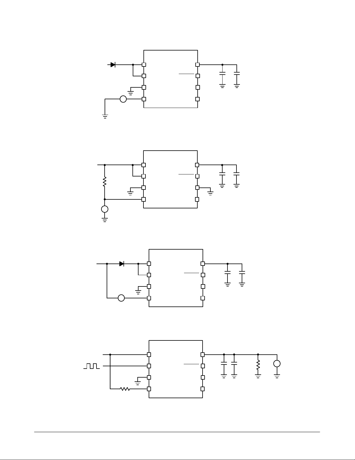
TEST CIRCUITS
t
rec(min)
t
rec(max)
58.1%
28.4%
V
SUP
R
L
V
SUP
EN
GND
BUS
V
OUT
RESET
TxD
RxD
10 F
+
50 pF
C
L
Figure 5. Test Circuit for Delay Time, Slope Time, and Duty Cycle
NCV7361A
NCV7361A
V
SUP
EN
GND
BUS
V
OUT
RESET
TxD
RxD
10 F
+
12 V
IS1
A
+
100 nF
100 nF
Figure 6. T est Circuit for Supply Current I
http://onsemi.com
8
Snl
NCV7361A
TEST CIRCUITS (continued)
NCV7361A
V
BAT
V
EN
SUP
V
OUT
RESET
10 F
+
100 nF
V
V
BUSREC
GND
BUS
TxD
RxD
Figure 7. Test Circuit for Bus Voltage “Recessive’’
(V
BUSREC
)
NCV7361A
V
SUP
V
EN
SUP
V
OUT
RESET
500
GND
V
BUSD
V
BUS
TxD
RxD
Figure 8. T est Circuit for Bus Voltage “Dominant’’ V
NCV7361A
V
BAT
V
EN
SUP
V
OUT
RESET
10 F
+
BUSDOM
+
100 nF
10 F 100 nF
I
INBUSR
A
Figure 9. Test Circuit for Bus Current “Recessive’’ I
13.5 V
Figure 10. T est Circuit for V
GND
BUS
TxD
RxD
INBUSR
NCV7361A
V
SUP
EN
GND
BUS
Rise Time vs. Load Capacitance and Resistance
OUT
V
OUT
RESET
TxD
RxD
C
VAR
100 nF V
+
http://onsemi.com
9
V
R
L
OUT

NCV7361A
TYPICAL OPERATING CHARACTERISTICS
Figure 11. V
Rise Time with 1 F, 10 F,
out
100 F, and 150 F Capacitors and 200 Load
using EN to Enable the Output.
Figure 13. V
Rise Time with a 100 F Load
out
Capacitor and 1 k, 200 , and 100 Load
using EN to Enable the Output.
Figure 12. V
Rise Time with a 10 F Load
out
Capacitor and 1 k, 200 , and 100 Load
using EN to Enable the Output.
Figure 14. V
Rise Time with a 150 F Load
out
Capacitor and 1 k, 200 , and 100 Load
using EN to Enable the Output.
http://onsemi.com
10

NCV7361A
FUNCTIONAL DESCRIPTION
The NCV7361A consists of a low drop voltage regulator
5.0 V/50 mA and a LIN Bus transceiver, which is a
bidirectional bus interface for data transfer between the
LIN bus and the LIN protocol controller.
Additionally, the NCV7361A features a RESET output
with a reset delay of 100 ms and a fixed threshold of 4.65 V
and Enable (EN) control for the regulator.
V
POWER ON
SUP
Clear All State−FF
V
> UVR_OFF
POR
V
SUP
< UVR_ON
SUP
V
< UVR_ON
SUP
V
> UVR_OFF and
SUP
(EN = L/H or Bus Wake−Up)
Ini−state
Operating Modes
The NCV7361A provides two main operating modes
“normal” and “sleep” and the intermediate states “POR”,
“Ini−state” and “thermal shutdown”. The main modes are
fixed states defined by basic actions (V
start, EN or
SUP
wake−up). The intermediate states are soft states. They
aren’t defined by logical actions but by changes of voltage
(V
, V
SUP
Clear RESET Timer
Regulator ON V
RESET = L
Wake−Up Disabled
V
< V
OUT
RES
) or junction temperature.
OUT
Ramp Up
OUT
V
> V
OUT
(4.65 V)
RES
Normal
Mode
EN = H
Regulator ON
RESET = L after 100 ms
RESET = H
Wake−Up Disabled
LIN Transceiver ON
EN = H/L
EN = L
Sleep
Mode
Regulator OFF
Wake−Up Enabled (LIN Receiver ON)
LIN Transmitter OFF
Sleep Mode and
TJ < T
JREC
Sleep Mode and
TJ < T
JSHD
TJ < T
JREC
Figure 15. State Diagram of Operating Modes
Normal Mode
The whole NCV7361A is active. Switching to normal
mode can be done via the following actions:
• Start of V
or after Undervoltage Reset
SUP
• Rising Edge at EN (EN = High) (Local Wake−Up)
• Activity on the LIN Bus (Remote Wake−Up)
Normal Mode and
TJ < T
JREC
Normal Mode and
TJ > T
JSHD
Thermal
Shutdown
Regulator OFF
Wake−Up Disabled
LIN Transceiver OFF
Sleep Mode
Sleep mode is most current saving. With a falling edge
on EN (EN = Low) the NCV7361A is switched from
normal mode into sleep mode. The voltage regulator will
be switched off and the LIN transceiver is in
recessive state.
http://onsemi.com
11

V
SUVR_OFF
V
SUVR_ON
V
NCV7361A
SUP
UVR
V
OUT
Figure 16. Operating of Power On and Undervoltage RESET
POR
Normal Mode Sleep Mode
Switching into sleep mode can be done independently
from the current transceiver state. That means if the
transmitter is in dominant state this state will be cancelled
and it will be switched to recessive state.
POR−state
This is the power−on−reset state of the NCV7361A,
while V
SUP
< V
SUVR_OFF
. If the prior state was sleep mode,
the NCV7361A switches via the Ini−state to normal mode.
Ini−state
This is an intermediate state, which will pass through
after switch−on of V
in this state if V
V
> V
SUP
Thermal Shutdown
OUT
SUVR_ON
If the junction temperature T
or V
SUP
is below V
.
. The NCV7361A remains
OUT
(Reset Output = L) and
RES
is higher than T
J
JSHD
(>155°C), the NCV7361A will be switched into the
thermal shutdown mode. The behavior within this mode is
comparable with the sleep mode except for LIN transceiver
operating. The transceiver is completely disabled, no
wake−up functionality is available.
If TJ falls below the thermal recovery temperature T
JREC
(typical 140°C) the NCV7361A will be recover to the
previous state (normal or sleep).
Initialization
Initialization is started if the power supply is switched on
as well as every rising edge on of the NCV7361A via the
EN pin.
V
− Power On
SUP
If V
is switched on the NCV7361A starts to normal
SUP
mode via the POR− and Ini−state. A combination of
dynamic POR and undervoltage reset circuitry generates a
POR signal, which switches the NCV7361A into normal
mode. This power on behavior is independent from the
status of the EN pin.
Power−on−Reset and undervoltage reset operates
independent from each other, which secures the
EN = H/L
independence from the rise time of V
POR
UVR
Normal Mode
. During fast V
SUP
edges the Power−on−Reset will be active. If the increasing
of V
initializes the voltage regulator if V
is very slow (> 1 ms/V) the undervoltage reset unit
SUP
> V
SUP
SUVR_OFF
(typical 3.5 V).
The effects of both POR circuits at different V
SUP
as shown in Figure 16.
After POR the voltage regulator starts and V
output. If V
If the V
OUT
t
= 100 ms is started. After t
Res
OUT
> V
the bus interface will be activated.
MRes
voltage level is higher than V
the RESET output
Res
OUT
, the reset time
RES
switches from low to high (Figure 16).
Start of Linear Regulator via Wake−Up
The initialization is only being done for the V
circuitry parts. This procedure begins with leaving the
master reset state (V
manner as the V
Wake−Up
SUP
> V
OUT
MRes
− Power−On.
) and runs in the same
If the regulator is put into sleep mode it can be
“waked−up” with the BUS interface. Every pulse on the
BUS (high pulse or low pulse) with a pulse width of
minimum 60 s switches on the regulator.
After the BUS has “waked−up” the regulator, it can only
be switched off with a high level followed by a low level
on the EN pin.
V
Undervoltage Reset
SUP
The undervoltage detection unit inhibit an undefined
behavior of the NCV7361A under low voltage condition.
If V
drops below V
SUP
SUVR_ON
(typical 3 V) the
undervoltage detection becomes active and the IC will be
switched to POR state. The following increasing of V
above V
SUVR_OFF
(typical 3.5 V) cancels this POR state
and the voltage regulator starts with the initialization
sequence.
V
Undervoltage in Normal Mode
SUP
Supply Voltages below V
SUVR_OFF
voltage regulator. The output voltage V
do not influence the
follows V
OUT
SUP
slopes
will be
OUT
SUP
SUP
.
http://onsemi.com
12

NCV7361A
V
Undervoltage in Sleep Mode
SUP
No exit from the sleep mode will take place if the V
voltage drops down to V
SUVR_ON
(typical 3.0 V). The
undervoltage reset becomes active (POR−state). As a result
of this operating, the sleep mode is left to the normal mode.
If V
rises again above V
SUP
SUVR_OFF
(typical 3.5 V), the
IC initializes the voltage regulator and continues to work
with the normal mode.
The undervoltage reset unit secures stable operating in
the undervoltage range of V
down to GND level. The
SUP
dynamic Power−On−Reset secures a defined internal state
independent from the duration of the V
drop, which
SUP
secures a stable restart.
Overtemperature Shutdown
If the junction temperature is 155°C < T
< 170°C the
J
overtemperature recognition will be activated and the
regulator voltage will be switched off. The V
OUT
drops down, the reset state is entered and the
bus−transceiver is switched off (recessive state).
After T
falls below 140°C the NCV7361A will be
J
initialized again (Figure 17) independently from the
voltage levels on EN and BUS. Within the thermal
shutdown mode the transceiver can not be switched to the
normal mode neither with local nor with remote wake−up.
The operation of the NCV7361A is possible between
T
(125°C) and the switch−off temperature, but small
Amax
parameter differences can appear.
After overtemperature switch−off the IC behaves as
described in Figure 17.
SUP
voltage
LIN BUS Transceiver
The NCV7361A is a bidirectional bus interface device
for data transfer between the LIN bus and the LIN protocol
controller.
The transceiver consists of a pnp−driver (1.2 V @
40 mA) with slew rate control, wave shaping and current
limit, and a high voltage receiver/comparator followed by
a filter circuit.
Transmit Mode
During transmission the data at the TxD pin will be
transferred to the BUS driver for generating a BUS signal.
To minimize the electromagnetic emission of the bus line,
the BUS driver has integrated slew rate control and wave
shaping circuitry.
Transmitting will be interrupted in the following cases:
• Sleep Mode
• Thermal Shutdown Active
• Master Reset (V
The recessive BUS level is generated from the integrated
30 k pullup resistor in series with a diode This diode
prevents reverse current on V
No additional termination resistor is necessary to use the
NCV7361A in LIN slave nodes. If this IC is used for LIN
master nodes, it is necessary to terminate the bus pin with
an external 1.0 k resistor in series with a diode to V
Receive Mode
The data signal from the BUS pin will be transferred
continuously to the pin RxD. Short spikes on the bus are
suppressed by the internal filter circuit ( = 2.8 s).
< 3.15 V)
OUT
BUS
when V
BUS
> V
SUP
.
BAT
.
V
SUP
V
OUT
V
RES
RESET
T>T
t
Res
Initialization Thermal
J
T<T
t
rr
shutdown
J
t<t
rr
t
Res
Spike V
SUP
Figure 17. RESET Behavior
http://onsemi.com
13
t
Res
Low voltage
V
SUP
t<t
Spike V
rr
t
Res
Current limitation
CC
active

BUS
V
SUP
60%
50%
40%
V
thr_max
V
thr_min
V
thr_hysVthr_cnt
NCV7361A
t < t
deb_BUS
RxD
Figure 18. Receive Mode Impulse Diagram
The receive threshold values V
symmetrical to 0.5*V
with a hysteresis of 0.135*V
SUP
The LIN specific receive threshold is between 0.4*V
and 0.6 * V
SUP
.
thr_max
and V
thr_min
are
SUP
SUP
Data Rate
The NCV7361A is a constant slew rate transceiver. The
bus driver works with a fixed slew rate range of 1.0 V/s
V/T 2.5 V/s. This principle provides good
symmetry of the slope times between recessive to dominant
and dominant to recessive slopes within the LIN bus load
range (C
BUS
, R
term
).
The NCV7361A guarantees data rates up to 20 kb within
the complete bus load range under worst case conditions.
t < t
deb_BUS
The constant slew rate principle holds appropriate voltage
.
levels and can operate within the LIN Protocol
Specification for RC oscillator systems with a matching
tolerance up to 2% between 2 nodes.
TxD Input
The 5.0 V input TxD directly controls the BUS level:
TxD = low → BUS = low (dominant level)
TxD = high → BUS = high (recessive level)
The TxD pin has an internal pullup resistor connected to
V
. This guarantees that an open TxD pin generates a
OUT
recessive BUS level.
V
V
CC
I
PU_TxD
R
PU_TxD
TxD
Typ.
15 k
OUT
RC Filter
(10 ns)
NCV7361AMCU
Figure 19. TxD Input Circuitry
http://onsemi.com
14

NCV7361A
RxD Output
The received BUS signal will be output to the 5.0 V RxD
pin:
BUS < V
BUS > V
This output is a push−pull driver between V
thr_cnt
thr_cnt
– 0.5 * V
+ 0.5 * V
→ RxD = low
thr_hys
→ RxD = high
thr_hys
OUT
and
GND with an output current capability of 1.0 mA.
NCV7361A MCU
V
OUT
RxD
Figure 20. RxD Output Circuitry
Linear Regulator
The NCV7361A has an integrated low dropout linear
regulator with a P−Channel MOSFET output driver whose
output is 5.0 V 2% at 50 mA and 5.5 V V
SUP
18 V. Figure 21 shows typical current limit based on the
output voltage.
120
100
80
(mA)
60
OUT
IV
40
20
0
05632
14
V
(V)
OUT
Figure 21. Characteristic of Current Limit
vs. Output Voltage
RESET
RESET switches from low to high if V
and V
If V
> V
OUT
OUT
RES
drops below V
for t
.
Res
, the RESET output goes from
RES
is switched on
SUP
high to low after trr. Short transients will be filtered.
The RESET output driver is driven from V
OUT
to
guarantee proper operation.
16
14
12
10
8
6
lol_RESET (mA)
4
2
0
0 0.5 1.0 1.5 2.0 3.0 3.5 4.0 4.52.5
V
(V)
OUT
Figure 22. Output Current of Reset Output vs.
Voltage
V
OUT
Initialization
The initialization is started if V
is switched on. This
SUP
is independent of the EN pin.
V
Power ON
SUP
The NCV7361A starts in the normal mode when V
applied [>3.15 V (typical)]. The internal circuitry on V
SUP
is
OUT
as well as the internal regulator starts the initialization with
power−on−reset. The voltage regulator is switched on.
If V
If V
is started. After t
> V
OUT
OUT
POR
is higher than V
the bus−interface will be activated.
, the reset time t
Res
the RESET output switches from low
Res
= 100 ms
Res
to high (Figure 22).
The initialization procedure at power on is started
independent from the EN state. The regulator can only be
turned off with a high level followed by a low level on the
EN pin.
Mode Input EN
The NCV7361A is switched into the sleep mode when
EN goes from high to low. The normal mode will be kept
as long as EN = high.
The regulator can be turned off by switching EN high to
low independent of the state of the bus−transceiver.
The EN input is internally pulled down to guarantee a
low with no connection. In the high state, the pulldown
current will be switched off to reduce the quiescent current.
The maximum input voltage is V
. The threshold is
SUP
typical 2.1 V and therefore CMOS levels can be used as
input signals. Figure 23 shows the internal circuitry of the
EN pin.
The EN input is internally pulled down to secure that if
this pin is not connected a low level will be generated. It
will be used two different pull down current sources for
high and low level to minimize the sleep mode current.
http://onsemi.com
15

NCV7361A
The 4 A pulldown current source is used if the input
voltage VIN > high level voltage V
drops below the low level of EN V
. If the input voltage
ENH
, the second current
ENL
source is used. The resulting pulldown current in this case
is 100 A.
V
SUP
Enable
EN
Voltage
Limiter
4 A
96 A
Figure 23. EN Input Circuitry
The wide input voltage range allows different EN control
possibilities. If the EN input is connected to an CMOS
output of the MCU, a falling edge switches the NCV7361A
into sleep mode (the regulator is also switched off). The
wake−up is only possible via the bus line.
1000
100
(k)
IN
R
10
0
0 0.5 1.0 1.5 2.0 3.0 3.5 4.0 4.52.5
Figure 24. RIN Characteristics of EN Input
RIN_HL
RIN_LH
5.0
VIN (V)
V
BAT
LIN−BUS
V
BAT
MCU
NCV7361A
V
+
C
IN
200p
SUP
EN
GND
BUS
V
OUT
RESET
TxD
RxD
+
C
load
+5 V
Figure 25. EN Controlled via MCU
MCU
NCV7361A
V
+
C
IN
SUP
EN
GND
V
OUT
RESET
TxD
+5 V
LIN−BUS
BUS
200p
RxD
C
load
Figure 26. Permanent Normal Mode
http://onsemi.com
16
+

NCV7361A
If the application does not need the wake−up capability
of the NCV7361A, a direct connection EN to V
SUP
is
possible. In this case, the NCV7361A operates in
permanent normal mode. Also possible is the external
(outside of the module) control of the EN line via a V
BAT
signal.
Wake−Up
If the regulator is in a standby (sleep) mode, it can be
woken up with the BUS interface. Every pulse on the BUS
(high pulse or low pulse) with a pulse width of minimum
25 s switches on the regulator.
After the BUS wake−up for the regulator, it can only be
turned off with a high level followed by a low level on the
EN pin.
Overtemperature Shutdown
The thermal shutdown threshold is 155°C < TJ < 175°C.
When exceeded, the overtemperature shutdown will be
active and the regulator voltage will be switched off. V
OUT
drops down, the reset state is entered and the
bus−transceiver is switched off (recessive state).
After TJ falls below 140°C, the NCV7361A will be
initialized (see Figure 17), independent from the voltage
levels on EN and BUS. W ithin the thermal shutdown mode,
the transceiver can’t be switched to the normal mode with
local or with remote wake−up.
Function of the NCV7361A is possible between T
Amax
(125°C) and the switch−off temperature, but small
parameter differences can appear.
After overtemperature switch−off the IC behaves as
described in the RESET chapter.
http://onsemi.com
17

LIN System Parameter
Bus Loading Requirements
NCV7361A
APPLICATION HINTS
Parameter Symbol Min Typ Max Unit
Operating Voltage Range V
Voltage Drop of Reverse Protection Diode V
Voltage Drop at the Series Diode in Pull Up Path V
Battery Shift Voltage V
Ground Shift Voltage V
Master Termination Resistor R
Slave Termination Resistor R
Number of System Nodes N 2 − 16 −
Total Length of Bus Line LEN
Line Capacitance C
Capacitance of Master Node C
Capacitance of Slave Node C
Total Capacitance of the Bus including Slave and Master Capacitance C
Network Total Resistance R
Time Constant of Overall System 1.0 − 5.0 s
Recommendations for System Design
The goal of the LIN physical layer standard is to have a
universal definition of the LIN system for plug and play
solutions in LIN networks up to 20 kbd bus speeds.
In case of small and medium LIN networks, it’s
recommended to adjust the total network capacitance to at
least 4.0 nF for good EMC and EMI behavior. This can be
done by setting only the master node capacitance. The
slave node capacitance should have a unit load of typically
220 pF for good EMC/EMI behavior.
In large networks with long bus lines and the maximum
number of nodes, some system parameters can exceed the
defined limits and the LIN system designer must intervene.
The whole capacitance of a slave node is not only the unit
load capacitor itself. Additionally, there is the capacitance
BAT
Drop_rev
SerDiode
Shift_BAT
Shift_GND
master
slave
BUS
LINE
Master
Slave
BUS
Network
than 700 . Even if the total network capacitance is below
or equal to the maximum specified value of 10 nF, the
network time constant is higher than 7.0 s.
This problem can be solved only by adjusting the master
termination resistor to the required maximum network time
constant of 5.0 s (max).
The LIN bus output driver of the NCV7361A provides a
higher drive capability than necessary (40 mA @ 1.2 V)
within the LIN standard (33.6 mA @ 1.2 V). With this
driver stage the system designer can increase the maximum
LIN networks with a total network capacitance of more
than 10 nF. The total network resistance can be
decreased to:
R
tl_min
of wires and connectors, and the internal capacitance of the
LIN transmitter. This internal capacitance is strongly
dependent on the technology of the IC manufacturer and
should be in the range of 30 pF to 150 pF. If the bus lines
have a total length of nearly 40m, the total bus capacitance
can exceed the LIN system limit of 10 nF.
A second parameter of concern is the integrated slave
termination resistor tolerance. If most of the slave nodes
have a slave termination resistance near by the allowed
maximum of 60 k, the total network resistance is more
NOTE: The NCV7361A meets the requirements for
implementation in RC−based slave nodes. The LIN
Protocol Specification requires the deviation of the slave
node clock to the master node clock after synchronization
must not differ by more than 2%.
Setting the network time constant is necessary in large
networks (primary resistance) and also in small networks
(primary capacitance).
8.0 − 18 V
0.4 0.7 1.0 V
0.4 0.7 1.0 V
0 − 0.1 V
0 − 0.1 V
900 1000 1100
20 30 60 k
− − 40 m
− 100 150 pF/m
− 220 − pF
− 220 250 pF
1.0 4.0 10 nF
537 − 863
(V
Bat_max
V
BUSdom
)I
BUS_max
(18 V 1.2 V)40mA 420
BAT
BAT
http://onsemi.com
18

BUS
NCV7361A
MIN/MAX SLOPE TIME CALCULATION
V
BUS
40%
t
100%
sdom
95%
V
0%
dom
Figure 27. Slope Time Calculation
5%
60%
t
srec
The slew rate of the bus voltage is measured between
40% and 60% of the output voltage swing (linear region).
The output voltage swing is the difference between
dominant and recessive bus voltage.
dVdt 0.2 * V
swing
(t
40%−t60%
)
The slope time is the extension of the slew rate tangent
until the upper and lower voltage swing limits:
t
slope
5*(t
40%−t60%
)
The slope t ime of the recessive t o d o minant e dge is directly
determined by the slew rate control of the transmitter:
t
slope
V
swing
dVdt
The dominant to recessive edge is influenced from the
network time constant and the slew rate control, because
it’s a passive edge. In case of low battery voltages and high
bus loads the rising edge is only determined by the network.
If the rising edge slew rate exceeds the value of the
dominant one, the slew rate control determines the rising
edge.
Power Dissipation and Operating Range
The max power dissipation depends on the thermal
resistance of the package and the PCB, the temperature
difference between Junction and Ambient as well as the
airflow.
The power dissipation can be calculated with:
PD (V
The power dissipation of the transmitter P
SUP
V
OUT
)*I
VOUT
P
D_TX
D_TX
depends
on the transceiver configuration and its parameters as well
as on the bus voltage V
BUS
= V
BAT
− V
, the resulting
D
termination resistance RL, the capacitive bus load CL and
the bit rate. Figure 28 shows the dependence of power
dissipation of the transmitter as function of V
SUP
. The
conditions for calculation the power dissipation was:
RL = 500 , CL = 10 nF, Bitrate = 20 kbit and duty cycle
on TxD of 50%.
50
45
35
30
25
(mW)
D
P
20
15
10
5
0
5
616197
V
SUP
1312111089
(V)
1740181514
Figure 28. Power Dissipation LIN Transceiver
@ 20 kbit
The permitted package power dissipation can be
calculated:
TJ T
P
If we consider that P
Dmax
D_TX_max
calculated the max output current IV
TJ−T
A
P
RJ−
I
VOUTmax
A
VSUP VOUT
A
RJ−
A
= f(V
OUT
D_TX_max
), it can be
SUP
on V
OUT
@ VSUP
:
TJ−TA is the temperature difference between junction
and ambient, and Rth is the thermal resistance of the
package. The thermal energy is transferred via the package
and the pins to the ambient. This transfer can be improved
with additional ground areas on the PCB as well as ground
areas under the IC.
http://onsemi.com
19

NCV7361A
Table 1. SO−8 Thermal RC Network Models*
54 mm
2
2
Copper Area (1 oz thick) 54 mm
(SPICE Deck Format) Cauer Network Foster Network
C_C1 Junction GND 1.08E−05 1.08E−05 W−s/C 1.00E−06 1.00E−06 sec
C_C2 node1 GND 4.10E−05 4.10E−05 W−s/C 1.00E−05 1.00E−05 sec
C_C3 node2 GND 1.13E−04 1.13E−04 W−s/C 1.00E−04 1.00E−04 sec
C_C4 node3 GND 4.42E−04 4.40E−04 W−s/C 5.00E−04 5.00E−04 sec
C_C5 node4 GND 1.74E−03 1.71E−03 W−s/C 1.00E−03 1.00E−03 sec
C_C6 node5 GND 1.39E−03 1.34E−03 W−s/C 1.00E−02 1.00E−02 sec
C_C7 node6 GND 2.08E−02 1.78E−02 W−s/C 1.00E−01 1.00E−01 sec
C_C8 node7 GND 1.08E−02 9.75E−03 W−s/C 1.00E+00 1.00E+00 sec
C_C9 node8 GND 1.14E−01 1.84E−01 W−s/C 1.00E+01 1.00E+01 sec
C_C10 node9 GND 8.11E−01 3.00E+00 W−s/C 5.00E+01 5.00E+01 sec
R_R1 Junction node1 0.119 0.119 C/W 0.070 0.070 C/W
R_R2 node1 node2 0.286 0.286 C/W 0.152 0.152 C/W
R_R3 node2 node3 0.857 0.859 C/W 0.481 0.481 C/W
R_R4 node3 node4 1.181 1.189 C/W 0.690 0.690 C/W
R_R5 node4 node5 1.241 1.276 C/W 0.584 0.584 C/W
R_R6 node5 node6 2.574 2.690 C/W 3.223 3.223 C/W
R_R7 node6 node7 18.065 21.708 C/W 0.823 0.823 C/W
R_R8 node7 node8 27.965 26.035 C/W 26.801 35.166 C/W
R_R9 node8 node9 80.896 49.821 C/W 63.710 52.538 C/W
R_R10 node9 GND 49.468 15.252 C/W 86.119 25.510 C/W
*Bold face items in the tables above represent the package without the external thermal system.
The Cauer networks generally have physical
significance and may be divided between nodes to separate
thermal behavior due to one portion of the network from
another. The Foster networks, though when sorted by time
constant (as above) bear a rough correlation with the Cauer
networks, are really only convenient mathematical models.
Cauer networks can be easily implemented using circuit
Junction
R
1
R
2
R
714 mm
714 mm
3
2
2
Units Tau Tau Units
2
54 mm
R’s R’s
714 mm
2
simulating tools, whereas Foster networks may be more
easily implemented using mathematical tools (for instance,
in a spreadsheet program), according to the following
formula:
R(t)
n
i 1
−ttau
R
1−e
i
i
R
n
Junction
C
1
Time constants are
Amplitudes of mathematical solution are
C
2
not
simple RC products.
C
3
not
the resistance values.
Figure 29. Grounded Capacitor Thermal Network (“Cauer” Ladder)
R
1
C
1
Each rung is exactly characterized by its RC−product time constant; Amplitudes are the resistances
R
2
C
2
R
3
C
3
Figure 30. Non−Grounded Capacitor Thermal Ladder (“Foster” Ladder)
http://onsemi.com
20
C
n
Ambient
(thermal ground)
R
n
C
n
Ambient
(thermal ground)

NCV7361A
190
180
170
160
150
(°C/W)
140
JA
130
120
110
100
0 100 200 300 400 500 600 800
1000
100
2.0 oz. Cu
1.0 oz. Cu
700
Copper Area (mm2)
Figure 31. SO−8, JA as a Function of the Pad Copper Area Including Traces,
Board Material
Cu Area = 53.9 mm2 1.0 oz.
Cu Area = 89.7 mm2 1.0 oz.
10
(°C/W)
R
1
0.1
0.01
0.000001 0.00001 0.0001 0.001 0.01 0.1 1 10 100 1000
Time (s)
Cu Area = 713.9 mm21.0 oz.
Figure 32. SO−8 Thermal Transient Response on Typical Test Boards
1000
Cu Area = 713.9 mm21.0 oz.
50% Duty Cycle
100
10%
10
5%
2%
(°C/W)
1
R
1%
0.1
Single Pulse
EFFECTIVE THERMAL RESISTANCE
0.01
0.000001 0.00001 0.0001 0.001 0.01 0.1 1 10 100 1000
Time (s)
Notes:
P
DM
t
1
t
2
Duty Cycle, D =
t
1
t
2
Figure 33. SO−8 Thermal Duty Cycle Curves on 1.0 in. Spreader Test Board
http://onsemi.com
21

NCV7361A
60
5
616197
maximum current
SOIC8
TA = 125°C
TJ = 150°C
SOIC8
TA = 85°C
TJ = 125°C
V
(V)
SUP
Figure 34. Safe Operating Area
SOIC8
TA = 85°C
TJ = 150°C
1312111089
max. supply voltage
1740181514
50
(mA)
30
VCC_max
I
20
10
0
The linear regulator of the NCV7361A operates with
input voltages up to 18 V and can output a current of
50 mA. The maximum power dissipation limits the
maximum output current at high input voltages and high
ambient temperatures. The output current of 50 mA at an
ambient temperature of TA = 125°C is only possible with
small voltage differences between V
and VCC. See
SUP
Figure 34 for safe operating areas for different ambient and
junction temperatures.
Regulator Circuitry
Low Dropout Regulator
The voltage regulator of the NCV7361A is a low dropout
regulator (LDO) with a P−MOSFET as the
driving transistor.
This type of regulator has a standard pole, generated
from the internal frequency compensation and an
additional pole, which is dependent from the load and the
load capacity. This additional pole can cause an instable
behavior of the regulator! It requires a zero point to
compensate this additional pole. It can be realized via an
additional load resistor in series with a load capacity. It is
used for this compensation the
Equivalent Series Resistance (ESR) of the load capacity.
Every real capacity is characterized with an ESR value.
With the help of this ESR value an additional zero point is
implemented into the amplification loop and therefore the
result of the negative phase shift is compensated.
Because of this correlation the regulator has a stable
operating area which is defined by the load resistance RL,
the load capacity C
and the corresponding ESR value. The
L
load resistance resp. load current is defined by the
application itself and therefore the compensation of the
pole can only be done via variation of the load capacity and
ESR value.
Input Capacity on V
It is necessary to have an input capacity of C
SUP CIN
= 4.7 F.
IN
Higher capacity values improve the line transient response
and the supply noise rejection behavior. The combination
of electrolytic capacity (e.g.100 F) in parallel with a
ceramic RF−capacity (e.g. 100 nF) archives good
disturbance suppressing.
The input capacity should be placed as close as possible
(< 1 cm) to the V
Load Capacity on V
SUP
pin.
OUT CL
The regulator is stabilized by the output capacitor CL.
The NCV7361A requires a minimum of 4.7 F capacity
connected to the 5.0 V output to insure stability. This
capacitor should maintain its ESR in the stable region of the
ESR curve (Figure 35) over the full operating temperature
range of the application. The capacity value and the ESR
of a capacitor changes with temperature. The minimal
capacity value must be kept within the whole operating
temperature range.
Example 1:
The regulator is stabilized using a 47 F aluminum
electrolytic capacitor load (ESR = 0.7 @ 25°C). The
capacitance decreases to 42 F and the ESR increases to
8.9 at an ambient temperature of −40°C. The ESR value
is located in the unstable region. The regulator will be
unstable at −40°C.
Example 2:
The regulator is stabilized using a 47 F tantalum
capacitor load (ESR = 0.1 @ 25°C). The capacitance
decreases to 45 F and the ESR increases to 0.11 at an
ambient temperature of −40°C. The ESR value is located
in the stable region. The regulator will be stable at −40°C.
100
10
1
0.1
ESR @ 100 kHz (Ohm)
0.01
0
Figure 35. ESR Curves for 6.8 F CL 100 F and
Unstable Region
Stable Region
Unstable Region
40 50302010
Load Current (mA)
Frequency of 100 kHz
The value and type of the output capacitor can be
selected by using the diagram shown in Figure 35.
http://onsemi.com
22

NCV7361A
Capacity Value
The capacity value of an electrolytic capacitor is
dependence from the voltage, temperature and the
frequency. The temperature coefficient of the capacity
value is positive, that means that the value increases with
increasing of the temperature. The capacity value
decreases with increasing of the frequency. This behavior
of a capacitor can cause that at TA = −40°C the capacity
value falls below the minimum required capacity for the
regulator. In this case the regulator becomes instable,
which means the regulator starts oscillation. The nominal
value of the capacitor at TA = 25°C has to be chosen with
enough margin under consideration of the capacitor
specification. The instable behavior will be amplified
because of the decreasing of the capacity with this
oscillation.
ESR
The Equivalent Serial Resistance is the resistor part of
the equivalent circuit diagram of a capacitor. The ESR
value is dependent from the temperature and frequency.
Reverse
Protection−Diode
V
BAT
100 F
+
100 nF
NCV7361A
V
SUP
EN
GND
Normally the specified ESR values for a capacitor is valid
at a temperature of TA = 25°C and a frequency of
f = 100 kHz.
The temperature coefficient is negative, which means
with increasing of the temperature the ESR value
decreases. In the choice of the capacity has to be taken into
account that the ESR can decrease at TA = −40°C
dramatically that the valid operating area can be left, which
causes that the regulator will be instable.
T antalum Capacitors
This type of capacitor has a low dependence of the
capacity and the ESR from the temperature and is therefore
well suitable as V
Aluminum Capacitors
load capacity.
OUT
These capacitors show a strong influence of the capacity
and the ESR from the temperature. These characteristic
restrains the usability as load capacity for the low drop
regulator of NCV7361A.
C
V
OUT
RESET
TxD
+5 V
LIN−BUS
EMI Suppressing
10
RC−Filter
220 pF
or
Optional
100 p
Figure 36. Application Circuit (Slave Node)
BUS
33 H
LC−Filter
To minimize the influence of EMI from the bus line, a
220 pF capacitor should be directly connected to the BUS
pin (see Figure 36).
The value of the filter capacity can be adjusted to the size
of the LIN network. 220 pF should be used for bigger
networks. Values from 333 pF up to 1.0 nF should be used
for middle to small LIN networks. Finally the size of the
RxD
+
100 nF10 F...100 F
82p
filter capacitor influences the effectiveness of the EMI
suppressing in conformance to the maximum LIN bus
capacity of 10 nF.
LC−filters or RC−filters can also be used. The value of
C, L or R, depends on the corner frequency, the maximum
LIN bus capacity (10 nF) and the compliance with the DC−
and AC LIN bus parameters.
http://onsemi.com
23

NCV7361A
V
BAT
Master Node
LIN−BUS
100F
+
220pF
+
100nF
100nF
1 k
100nF
1k
V
IN
GND
NCV7380*
NC
VS
BUS
GND
NCV7361A
V
SUP
EN
GND
BUS
V
OUT
+
100F 100nF
+5 V
100nF
RxD
P
NC
V
CC
TxD
100nF
V
OUT
RESET
TxD
+5 V
C
RxD
220pF
+
Slave Node
*Not representative of actual pinout.
100F 100nF
Figure 37. Application Circuit for LIN Sub−Bus with NCV7361A as Slave Node
http://onsemi.com
24

NCV7361A
Connection to Flash−MCU
During programming of a flash MCU the NCV7361A
should be disconnected from the MCU. This can be done
by disconnecting the supply voltage of the NCV7361A or
by turning off the NCV7361A with the EN pin. A blocking
10F...47F
NCV7361A
V
OUT
RESET
TxD
RxD
V
V
Figure 38. Example Circuitry for Connection of RxD to MCU for Flash Programming
> 4.7 V at VDD = 5 V
high_RxD
= 0.8 V
low_RxD
diode must be used between the MCU and the RxD pin to
avoid loading of the programming data.
LIN pin, if the MCU supports this kind of flash mode.
Prog.−Data
+
47nF...100nF
0.7 V
The programming of the flash is also possible via the
C
V
= 4 V at VDD = 5 V
high
Operating During Disturbance
Operating Without V
SUP
or GND
The BUS pin is designed for voltages of GND − 24 V up
to GND + 30 V. This prevents loss of communication
between other bus nodes with the loss of V
GND. The BUS pin will remain at V
BAT
will be minimal with the loss of GND or V
Short Circuit BUS to V
BAT
or loss of
SUP
and current draw
.
SUP
• Recessive LIN bus is blocked, no influence to the
NCV7361A
• Dominant Current limit, thermal shutdown of
NCV7361A if power dissipation raises T
Short Circuit BUS to GND
The LIN bus is blocked. There is no influence to the
NCV7361A.
Short Circuit TxD to GND
The LIN transceiver is permanent in the dominant state
as is the LIN bus. This state can only be detected from the
LIN controller. In this case the controller must switch−off
the LIN node via the EN input of the NCV7361A and look
for a recessive state. A thermal shutdown of NCV7361A
will appear if the thermal shutdown threshold is exceeded.
TxD Open
The internal pullup resistor forces the LIN node to the
recessive state. The communication between the other
bus−nodes will not be disturbed.
Short Circuit V
The V
OUT
to GND
OUT
pin is protected via a current limit. This state
is comparable with the behavior in the sleep mode.
Overload of V
Thermal Switch−Off
OUT
The power dissipation is increasing if the load current is
between I
VOUT_max
and I
. If the IC exceeds the
LVOUT
thermal shutdown threshold of > 155°C, the transceiver
will be switched off. The voltage regulator will also be
switched off and a reset signal is forced.
Overcurrent
J
If the current limit is active the voltage on V
down. If this voltage is below the threshold V
will be forced.
Undervoltage V
SUP
, V
OUT
The reset circuit guarantees the correct behavior of the
driver during undervoltage. The BUS pin generates the
recessive state if V
OUT
< V
. The inputs EN and TxD
MRes
have pull−down and pull−up circuits respectively.
If V
MRes
V
4.5 V the TxD signal is transmitted
OUT
to the bus. The receive mode is also active.
Short Circuit RxD, RESET to GND or V
Both outputs are short circuit proof to V
OUT
OUT
drops
OUT
a reset
RES,
and ground.
http://onsemi.com
25

NCV7361A
ESD/EMC Remarks
General Remarks
Electronic semiconductor products are sensitive to
Electro Static Discharge (ESD). Always observe Electro
Static Discharge control procedures whenever handling
semiconductor products.
POWER SUPPLY PIN V
Test Pulse Condition Duration
1 t1 = 5.0 s/US = −100 V/tD = 2.0 ms 5000 Pulses
2 t1 = 0.5 s/US = 100 V/tD = 0.05 ms 5000 Pulses
3a/b US = −150 V/US = 100 V
5 Ri = 0.5 , tD = 400 ms
DA TA AND SIGNAL PINS EN, BUS
Test Pulse Condition Duration
1 t1 = 5.0 s/US = −100 V/tD = 2.0 ms 1000 Pulses
2 t1 = 0.5 s/US = 100 V/tD = 0.05 ms 1000 Pulses
3a/b US = −150 V/US = 100 V
SUP
Burst 100 ns/10 ms/90 ms Break
tr = 0.1 ms/UP + US = 40 V
Burst 100 ns/10 ms/90 ms Break
ESD Test
The NCV7361A is tested according to MIL883−3015.7
(Human Body Model).
EMC
The test on EMC impacts is done according to ISO
7637−1 for power supply pins and ISO 7637−3 for data and
signal pins.
1 h
10 Pulses Every 1 Min
1000 Burst
http://onsemi.com
26

−Y−
−Z−
NCV7361A
PACKAGE DIMENSIONS
SOIC−8 NB
D SUFFIX
CASE 751−07
ISSUE AC
−X−
B
H
A
58
1
4
G
D
0.25 (0.010) Z
M
S
Y
0.25 (0.010)
C
SEATING
PLANE
SXS
M
0.10 (0.004)
M
Y
K
N
X 45
M
J
NOTES:
1. DIMENSIONING AND TOLERANCING PER
ANSI Y14.5M, 1982.
2. CONTROLLING DIMENSION: MILLIMETER.
3. DIMENSION A AND B DO NOT INCLUDE
MOLD PROTRUSION.
4. MAXIMUM MOLD PROTRUSION 0.15 (0.006)
PER SIDE.
5. DIMENSION D DOES NOT INCLUDE DAMBAR
PROTRUSION. ALLOWABLE DAMBAR
PROTRUSION SHALL BE 0.127 (0.005) TOTAL
IN EXCESS OF THE D DIMENSION AT
MAXIMUM MATERIAL CONDITION.
6. 751−01 THRU 751−06 ARE OBSOLETE. NEW
STANDARD IS 751−07.
MILLIMETERS
DIMAMIN MAX MIN MAX
4.80 5.00 0.189 0.197
B 3.80 4.00 0.150 0.157
C 1.35 1.75 0.053 0.069
D 0.33 0.51 0.013 0.020
G 1.27 BSC 0.050 BSC
H 0.10 0.25 0.004 0.010
J 0.19 0.25 0.007 0.010
K 0.40 1.27 0.016 0.050
M 0 8 0 8
N 0.25 0.50 0.010 0.020
S 5.80 6.20 0.228 0.244
INCHES
SOLDERING FOOTPRINT
7.0
0.275
0.6
0.024
1.52
0.060
4.0
0.155
1.270
0.050
SCALE 6:1
mm
inches
http://onsemi.com
27

NCV7361A
ON Semiconductor and are registered trademarks of Semiconductor Components Industries, LLC (SCILLC). SCILLC reserves the right to make changes without further notice
to any products herein. SCILLC makes no warranty, representation or guarantee regarding the suitability of its products for any particular purpose, nor does SCILLC assume any
liability arising out of the application or use of any product or circuit, and specifically disclaims any and all liability, including without limitation special, consequential or incidental
damages. “Typical” parameters which may be provided in SCILLC data sheets and/or specifications can and do vary in different applications and actual performance may vary over
time. All operating parameters, including “Typicals” must be validated for each customer application by customer’s technical experts. SCILLC does not convey any license under
its patent rights nor the rights of others. SCILLC products are not designed, intended, or authorized for use as components in systems intended for surgical implant into the body,
or other applications intended to support or sustain life, or for any other application in which the failure of the SCILLC product could create a situation where personal injury or death
may occur. Should Buyer purchase or use SCILLC products for any such unintended or unauthorized application, Buyer shall indemnify and hold SCILLC and its officers, employees,
subsidiaries, affiliates, and distributors harmless against all claims, costs, damages, and expenses, and reasonable attorney fees arising out of, directly or indirectly, any claim of
personal injury or death associated with such unintended or unauthorized use, even if such claim alleges that SCILLC was negligent regarding the design or manufacture of the part.
SCILLC is an Equal Opportunity/Affirmative Action Employer. This literature is subject to all applicable copyright laws and is not for resale in any manner.
PUBLICATION ORDERING INFORMATION
LITERATURE FULFILLMENT:
Literature Distribution Center for ON Semiconductor
P.O. Box 61312, Phoenix, Arizona 85082−1312 USA
Phone: 480−829−7710 or 800−344−3860 Toll Free USA/Canada
Fax: 480−829−7709 or 800−344−3867 Toll Free USA/Canada
Email: orderlit@onsemi.com
N. American Technical Support: 800−282−9855 Toll Free
USA/Canada
Japan: ON Semiconductor, Japan Customer Focus Center
2−9−1 Kamimeguro, Meguro−ku, Tokyo, Japan 153−0051
Phone: 81−3−5773−3850
http://onsemi.com
ON Semiconductor Website: http://onsemi.com
Order Literature: http://www.onsemi.com/litorder
For additional information, please contact your
local Sales Representative.
NCV7361A/D
28
 Loading...