

ON Semiconductor NCP5662, NCV5662 Technical data
NCP5662, NCV5662
Low Output Voltage,
Ultra-Fast 2.0 A Low Dropout
Linear Regulator with Enable
The NCP5662/NCV5662 is a high performance, low dropout linear
regulator designed for high power applications that require up to 2.0 A
current. It is offered in both fixed and adjustable output versions. With
output voltages as low as 0.9 V and ultra-fast response times for load
transients, the NCP5662/NCV5662 also provides additional features
such as Enable and Error Flag (for the fixed output version),
increasing the utility of these devices. A thermally robust, 5 pin
2
D
PAK or DFN8 package, combined with an architecture that offers
low ground current (independent of load), provides for a superior
high-current LDO solution.
Features
•Ultra-Fast Transient Response (Settling Time: 1-3 ms)
•Low Noise Without Bypass Capacitor (26 mV
•Low Ground Current Independent of Load (3.0 mA Maximum)
•Fixed/Adjustable Output Voltage Versions
•Enable Function
•Error Flag (Fixed Output Version)
•Current Limit Protection
•Thermal Shutdown Protection (160°C)
•0.9 V Reference Voltage for Ultra-Low Output Operation
•Power Supply Rejection Ratio > 65 dB
•NCV Prefix for Automotive and Other Applications Requiring Site
and Control Changes
•These are Pb-Free Devices
Applications
•Servers
•ASIC Power Supplies
•Post Regulation for Power Supplies
•Constant Current Source
•Networking Equipment
•Gaming and STB Modules
rms)
http://onsemi.com
MARKING DIAGRAMS AND
PIN ASSIGNMENTS
Tab = GND
NC
1
5
D2PAK
DS SUFFIX
CASE 936AA
1
DFN8
MN SUFFIX
CASE 488AF
Fixed Version Adjustable Version
Pin 1 = EF
2 = GND
3 = N/C
4 = EN
5, 6 = V
7, 8 = V
x = P or V
y = A for Adjustable Version
A = Assembly Location
L = Wafer Lot
Y = Year
WW = Work Week
G or G = Pb-Free Package
(Note: Microdot may be in either location)
x5662DSy
AWLYWWG
1
in
out
B for Fixed 1.5 V Version
C for Fixed 3.3 V Version
D for Fixed 1.2 V Version
E for Fixed 1.8 V Version
F for Fixed 2.5 V Version
G for Fixed 2.8 V Version
H for Fixed 3.0 V Version
Pin 1 = EN
NCP5
662y
ALYWG
G
Pin 1 = ADJ
2 = GND
3 = N/C
4 = EN
5, 6 = V
7 = V
out
8 = N/C
2 = V
in
3 = GND
4 = V
out
5 = ADJ/EF
in
© Semiconductor Components Industries, LLC, 2007
October, 2007 - Rev. 9
ORDERING INFORMATION
See detailed ordering and shipping information in the package
dimensions section on page 13 of this data sheet.
1 Publication Order Number:
NCP5662/D
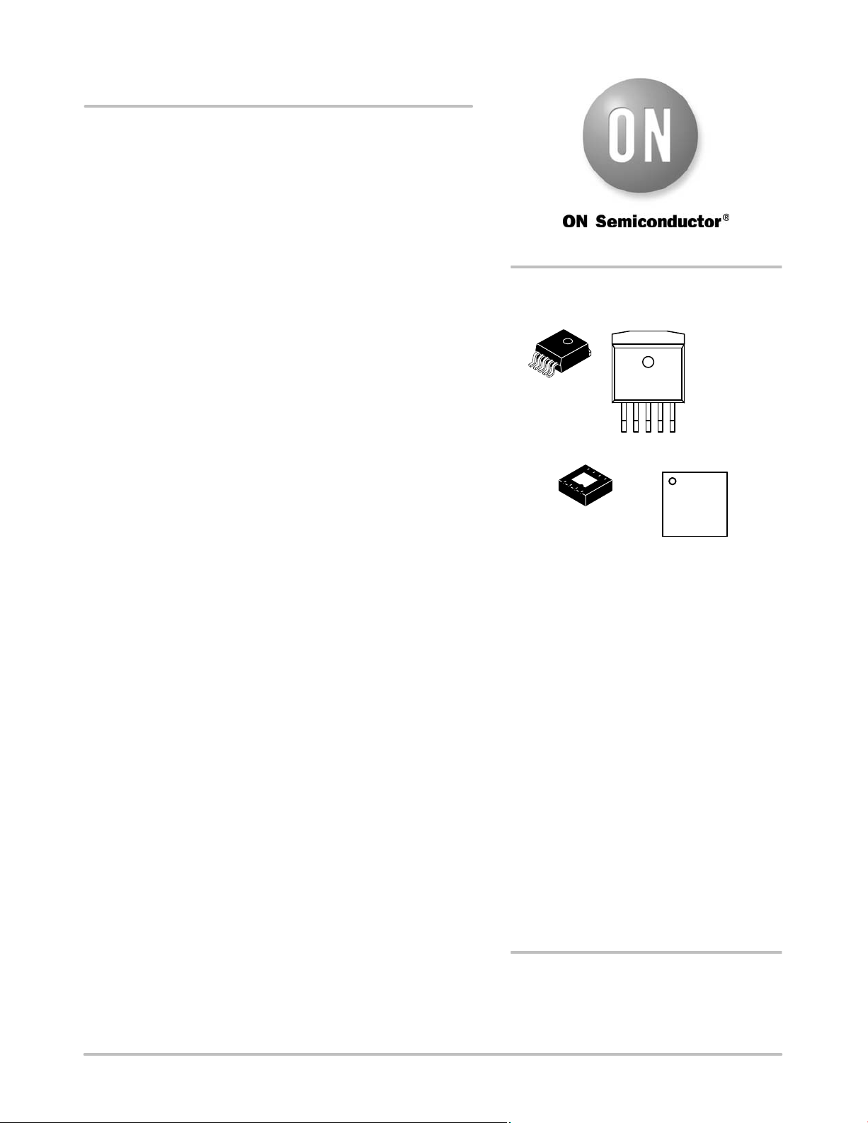
NCP5662, NCV5662
R
EF
V
in
V
in
NCP5662
V
out
NCV5662
EN
C
in
GND
EF
V
out
Error Flag
C
out
V
in
V
in
NCP5662
V
out
NCV5662
C
in
EN
ADJ
GND
R1
R2
V
out
C
out
Enable
ONOFF
Figure 1. Typical Application Schematic, Fixed
Output
Enable
ONOFF
Figure 2. Typical Application Schematic,
Adjustable Output
PIN FUNCTION DESCRIPTION
Pin
Adj/Fixed
2
PAK
D
1 4 EN Enable. This pin allows for on/off control of the regulator. To disable
2 5, 6* V
3, TAB 2 GND Power Supply Ground
4 7, 8 V
5 1 ADJ
5 1 EF
- 3, 8 Pin 3 N/C on Fixed & ADJ Version
- EPAD EPAD Exposed thermal pad should be connected to ground.
*Pins 5 and 6 must be connected together externally for output current full range operation.
Pin
Adj/Fixed
DFN8
Pin Name Description
in
out
(Adjustable Version)
(Fixed Version)
while Pin 8 N/C on ADJ Version only
the device, connect to Ground. If this function is not in use, connect
to V
.
in
Positive Power Supply Input Voltage
Regulated Output Voltage
This pin is connected to the resistor divider network and programs
the output voltage.
An Error Flag is triggered when the output voltage is out of regulation
excluding transient signals that may occur. Requires a pullup resistor
f 100 kW.
No connection. True no connect. PCB runs allowable.
http://onsemi.com
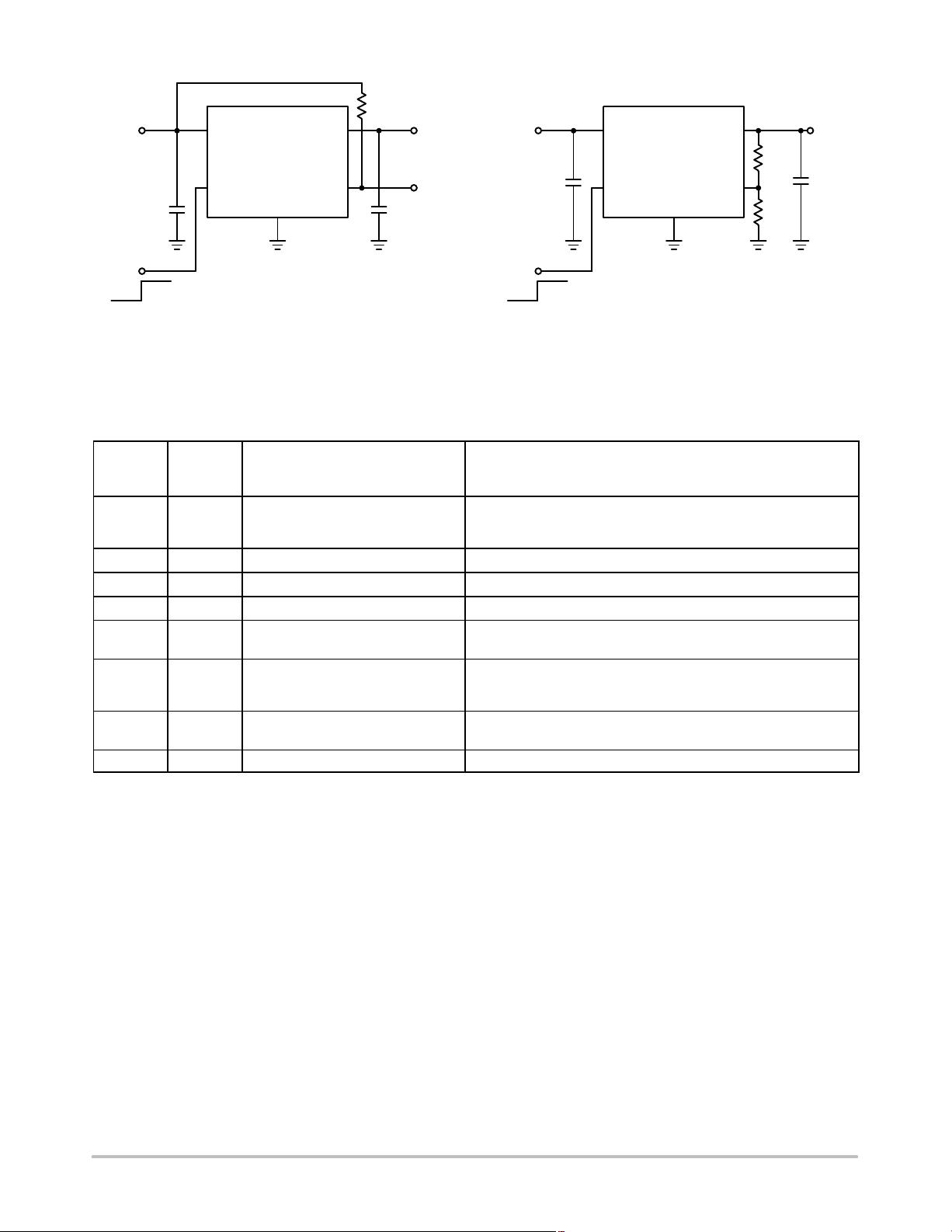
2
NCP5662, NCV5662
V
in
Voltage
Reference
Block
Enable
Block
R3
V
ref
= 0.9 V
Output
Stage
R4
Error
Flag
GND
Figure 3. Block Diagram, Fixed Output
V
in
R1
R2
Cc
V
EF
EN
out
Voltage
Reference
V
Block
R3
= 0.9 V
ref
Output
Stage
R4
GND
Figure 4. Block Diagram, Adjustable Output
Enable
Block
EN
V
out
ADJ
http://onsemi.com
3
NCP5662, NCV5662
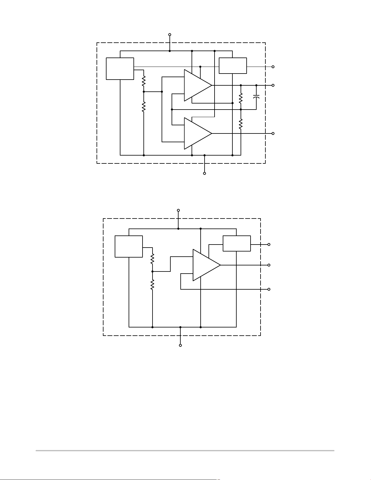
ABSOLUTE MAXIMUM RATINGS
Rating Symbol Value Unit
Input Voltage (Note 1) V
Output Pin Voltage V
Adjust Pin Voltage V
Enable Pin Voltage V
Error Flag Voltage V
Error Flag Current I
Maximum Junction Temperature T
in
out
ADJ
EN
EF
EF
J(max)
Stresses exceeding Maximum Ratings may damage the device. Maximum Ratings are stress ratings only. Functional operation above the
Recommended Operating Conditions is not implied. Extended exposure to stresses above the Recommended Operating Conditions may affect
device reliability.
NOTE: This device series contains ESD protection and exceeds the following tests:
Human Body Model (HBM) JESD 22-A114-B, passed 2000 V.
Machine Model (MM) JESD 22-A115-A, passed 200 V.
1. Refer to Electrical Characteristics and Application Information for Safe Operating Area.
THERMAL CHARACTERISTICS
Rating Symbol Value Unit
Thermal Characteristics, D2PAK (Notes 1 and 2)
Thermal Resistance, Junction-to-Ambient
Thermal Resistance, Junction-to-Case
Thermal Reference, Junction-to-Lead
Thermal Characteristics, DFN8 (Notes 1 and 2)
Thermal Resistance, Junction-to-Ambient
Thermal Reference, Junction-to-Lead (Note 3)
2. As measured using a copper heat spreading area of 1 sq in copper, 1 oz copper thickness.
3. Lead 6.
R
q
JA
R
q
JC
R
Y
JL
R
q
JA
R
Y
JL
18 V
-0.3 to (Vin +0.3) V
-0.3 to (Vin +0.3) V
-0.3 to (Vin +0.3) V
-0.3 to (Vin +0.3) V
3.0 mA
150 °C
°C/W
45
5.0
7.0
°C/W
78
14
OPERATING RANGES
Rating Symbol Value Unit
Operating Input Voltage (Note 1) V
Operating Ambient Temperature Range NCP5662
Storage Temperature Range T
4. Minimum Vin = (V
+ VDO) or 2 V, whichever is higher.
out
NCV5662
in
T
A
stg
(V
), 2 to 9 (Note 4) V
out+VDO
-40 to +85
-40 to +125
-55 to +150 °C
°C
http://onsemi.com
4
NCP5662, NCV5662
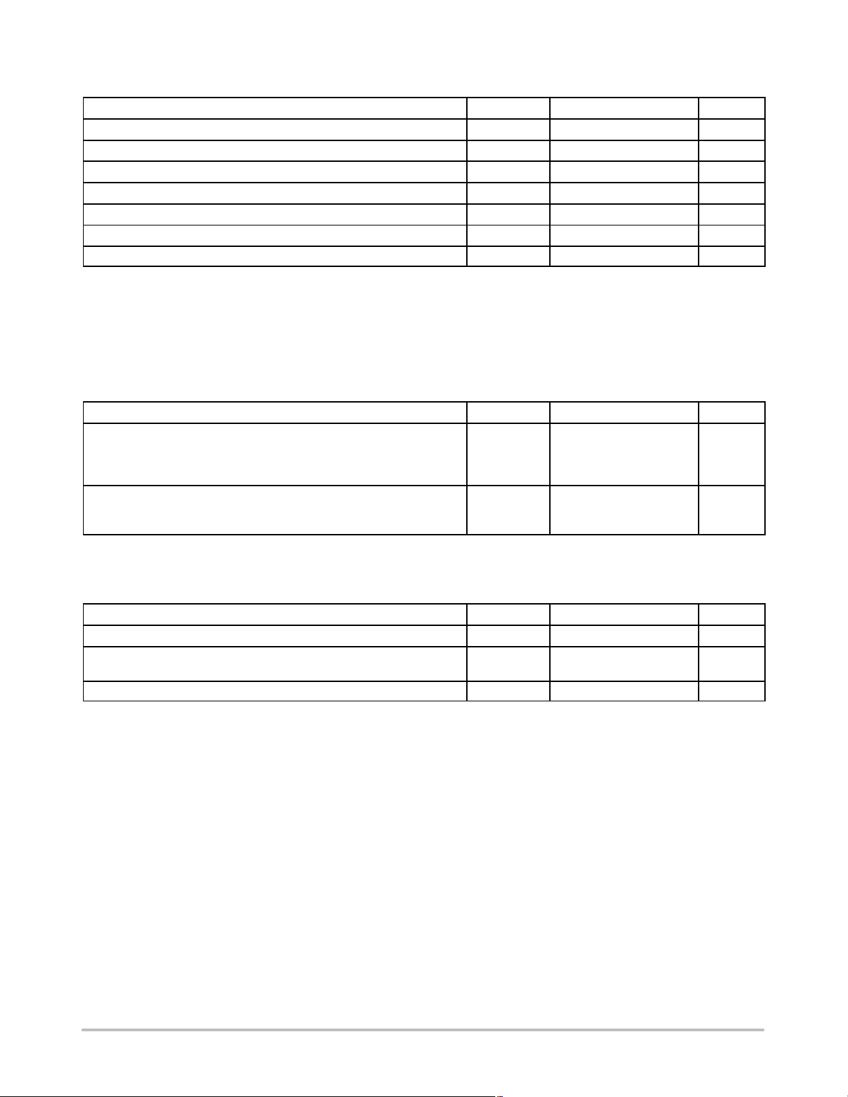
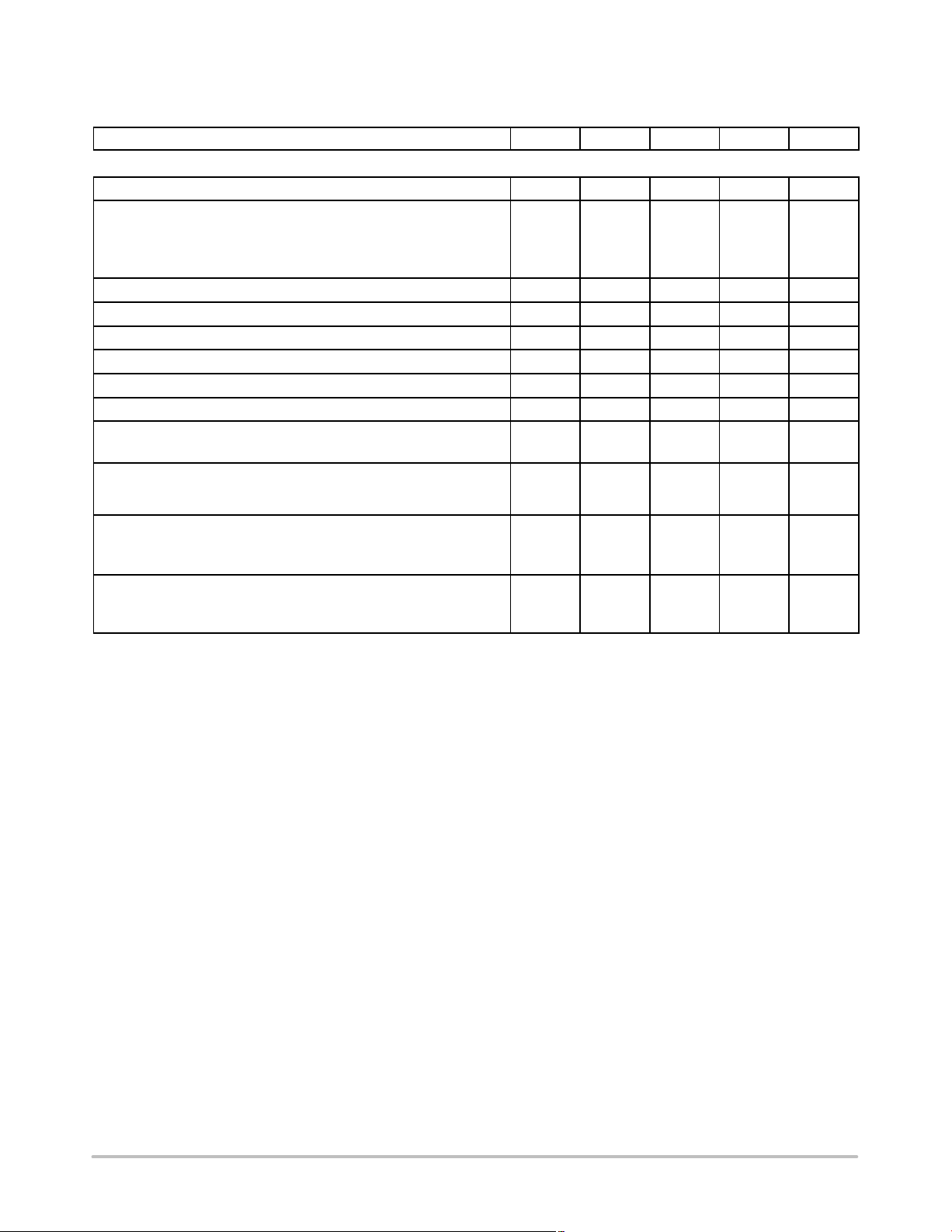
ELECTRICAL CHARACTERISTICS (V
version), TA = -40°C to 125°C (NCV version), Cin = C
Characteristic
= V
+ 1.5 V, for typical values TA = 25°C, for min/max values TA = -40°C to 85°C (NCP
in
out
= 150 mF unless otherwise noted. (Note 5))
out
Symbol Min Typ Max Unit
ADJUSTABLE OUTPUT VERSION
Output Noise Voltage
Output Voltage
T
= 25°C (V
A
T
= -20 to +125°C (V
A
T
= -40 to +150°C (V
A
= V
in
out
+1.5 V to 7.0 V, I
= V
+1.5 V to 7.0 V, I
in
out
= V
+1.5 V to 7.0 V, I
in
out
= 10 mA to 2.0 A)
out
= 10 mA to 2.0 A)
out
= 10 mA to 2.0 A)
out
Adjustable Pin Input Current I
Line Regulation (I
Load Regulation (10 mA < I
Dropout Voltage (I
= 10 mA, V
out
= 2.0 A) V
out
+1.5 V < Vin < 7.0 V) REG
out
< 2.0 A) REG
out
Peak Output Current Limit I
Internal Current Limitation I
Ripple Rejection (120 Hz)
Ripple Rejection (1 kHz)
V
n
V
out
ADJ
line
load
DO
out(peak)
LIM
RR -
- 26 -
(-1%)
(-1.5%)
(-2%)
0.9
-
(+1%)
(+1.5%)
-
(+2%)
- 40 - nA
- 0.03 - %
- 0.03 - %
- 1.0 1.3 V
2.0 - - A
- 3.0 - A
70
-
65
-
-
mV
rms
V
dB
Ground Current
I
Enable Input Threshold Voltage
Enable Input Current
= 2.0 A
out
Disabled State
Voltage Increasing, On state, Logic High
Voltage Decreasing, Off state, Logic Low
Enable Pin Voltage = 0.3 V
Enable Pin Voltage = 1.3 V
max
min
I
GND
I
GND(DIS)
V
EN
I
EN
-
-
1.3
-
-
-
1.3
10
0.5
0.5
3.0
300
mA
mA
V
-
-
0.3
-
-
mA
-
5. Performance guaranteed over specified operating conditions by design, guard banded test limits, and/or characterization, production tested at
= TA = 25°C. Low duty cycle pulse techniques are used during testing to maintain the junction temperature as close to ambient as possible.
T
J
http://onsemi.com
5
 Loading...