

Page 1
查询NCV4279D1供应商
NCV4279
5.0 V Micropower 150 mA
LDO Linear Regulator with
DELAY, Adjustable RESET,
and Sense Output
The NCV4279 is a 5.0 V precision micropower voltage regulator
with an output current capability of 150 mA.
The output voltage is accurate within ±2.0% with a maximum
dropout voltage of 0.5 V at 100 mA. Low quiescent current is a feature
drawing only 150 mA with a 1.0 mA load. This part is ideal for any and
all battery operated microprocessor equipment.
Microprocessor control logic includes an active reset output RO
with delay and a SI/SO monitor which can be used to provide an early
warning signal to the microprocessor of a potential impending reset
signal. The use of the SI/SO monitor allows the microprocessor to
finish any signal processing before the reset shuts the microprocessor
down.
The active Reset circuit operates correctly at an output voltage as
low as 1.0 V. The Reset function is activated during the power up
sequence or during normal operation if the output voltage drops
outside the regulation limits.
The reset threshold voltage can be decreased by the connection of an
external resistor divider to the R
against reverse battery, short circuit, and thermal overload conditions.
The device can withstand load dump transients making it suitable for
use in automotive environments. The device has also been optimized
for EMC conditions.
If the application requires pullup resistors at the logic outputs Reset
and Sense Out, the NCV4269 with integrated resistors can be used.
Features
• 5.0 V ± 2.0% Output
• Low 150 mA Quiescent Current
• Active Reset Output Low Down to V
• Adjustable Reset Threshold
• 150 mA Output Current Capability
• Fault Protection
♦ +60 V Peak Transient Voltage
♦ −40 V Reverse Voltage
♦ Short Circuit
♦ Thermal Overload
• Early Warning through SI/SO Leads
• Internally Fused Leads in SO−14 Package
• Very Low Dropout Voltage
• Electrical Parameters Guaranteed Over Entire Temperature Range
• Pb−Free Packages are Available
• NCV Prefix for Automotive and Other Applications Requiring Site
and Control Changes
lead. The regulator is protected
ADJ
= 1.0 V
Q
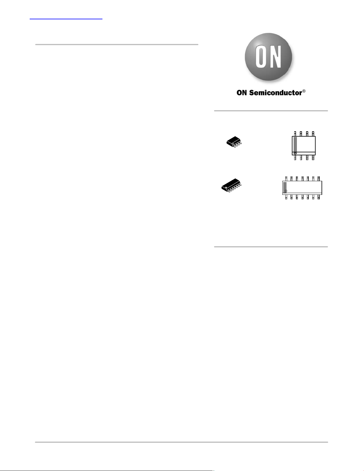
http://onsemi.com
MARKING
DIAGRAMS
8
1
14
1
A = Assembly Location
WL, L = Wafer Lot
YY, Y = Year
WW, W = Work Week
G, G = Lead Free Indicators
ORDERING INFORMATION
See detailed ordering and shipping information in the package
dimensions section on page 12 of this data sheet.
SO−8
D SUFFIX
CASE 751
SO−14
D SUFFIX
CASE 751A
8
1
14
NCV4279
AWLYWWG
1
4279
ALYW
G
© Semiconductor Components Industries, LLC, 2005
December, 2005 − Rev. 3
1 Publication Order Number:
NCV4279/D
Page 2
NCV4279
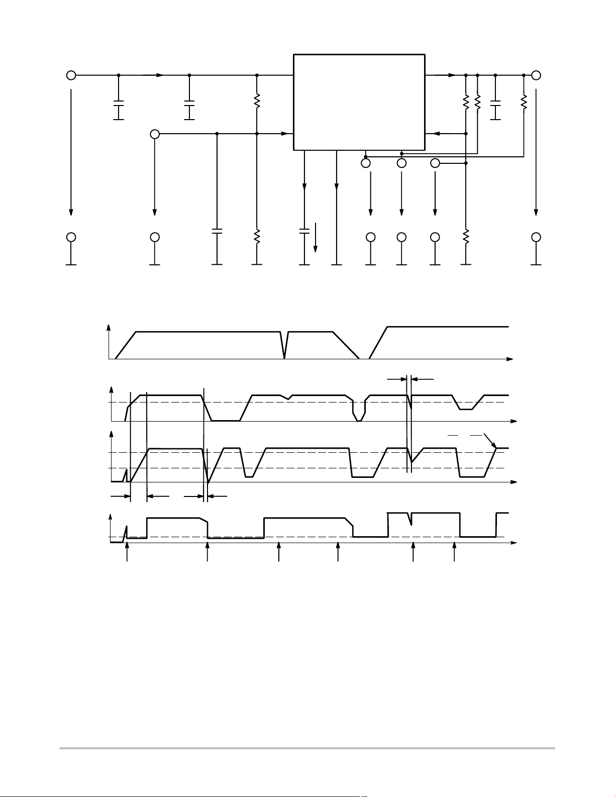
I
Reference
and Trim
D
or
R
ADJ
SI
Error
Amplifier
Current and
Saturation
Control
Reference
+
−
Q
RO
SO
GND
Figure 1. Block Diagram
PIN CONNECTIONS
18
ADJ
114
ADJ
QI
SOSI
ROR
GNDD
SIR
ID
GNDGND
GNDGND
GNDGND
QGND
SORO
SO−8
SO−14
PACKAGE PIN DESCRIPTION
Package Pin Number
SO−8 SO−14
3 1 R
4 2 D Reset Delay; To Set Time Delay, Connect to GND with a Capacitor
5 3, 4, 5, 6,
10, 11, 12
6 7 RO Reset Output; This is an Open−Collector Output. Leave Open if Not Used.
7 8 SO Sense Output; This is an Open−Collector Output. If not used, keep open.
8 9 Q
1 13 I Input; Connect to GND Directly at the IC with a Ceramic Capacitor.
2 14 SI Sense Input; If not used, Connect to Q.
Pin Symbol Function
ADJ
GND Ground
Reset Threshold Adjust; if not used to connect to GND.
5 V Output; Connect to GND with a 10 mF Capacitor, ESR < 10 W.
http://onsemi.com
2
Page 3
NCV4279
MAXIMUM RATINGS (T
= −40°C to 150°C)
J
Parameter
Symbol Min Max Unit
Input to Regulator V
Input Peak Transient Voltage V
Sense Input V
Reset Threshold Adjust V
Reset Delay V
Ground I
Reset Output V
Sense Output V
Regulated Output V
Junction Temperature
Storage Temperature
Input Voltage Operating Range
Junction Temperature Operating Range
Junction−to−Ambient Thermal Resistance SO−8
SO−14
I
RADJ
I
RADJ
I
I
RO
I
SO
I
T
T
STG
V
T
R
I
I
I
I
SI
SI
−40
Internally Limited45Internally Limited
− 60 V
−40
−1
−0.3
−10
−0.3
Internally Limited7Internally Limited
50 − mA
−0.3
Internally Limited7Internally Limited
−0.3
Internally Limited7Internally Limited
−0.5
−10
−
−50
−
−40
− 200
RO
SO
Q
q
D
D
q
Q
J
I
J
JA
45
1
7
10
7.0
−
150
150
45
150
70
V
V
mA
V
mA
V
V
V
V
mA
°C
°C
V
°C
k/W
Junction−to−Pin 4, all GND Pins Grounded. SO−14
R
q
JP
− 30 k/W
Lead Temperature Soldering and MSL
Parameter
Symbol Value Unit
MSL, 8−Lead, 14−Lead, LS Temperature 260°C Peak (Notes 3, 4) MSL 1 −
Maximum ratings are those values beyond which device damage can occur. Maximum ratings applied to the device are individual stress limit
values (not normal operating conditions) and are not valid simultaneously . If these limits are exceeded, device functional operation is not implied,
damage may occur and reliability may be affected.
1. This device series incorporates ESD protection and exceeds the following ratings:
Human Body Model (HBM) ≤ 2.0 kV per JEDEC standard: JESD22–A114.
Machine Model (MM) ≤ 200 V per JEDEC standard: JESD22–A115.
2. Latchup Current Maximum Rating: ≤ 150 mA per JEDEC standard: JESD78.
3. Lead free: 60−150 Sec above 217°C, 40 Sec Max at Peak, 265°C Peak.
4. Leaded; 60−150 Sec above 183°C, 30 Sec Max at Peak, 240°C Peak.
http://onsemi.com
3
Page 4
NCV4279
ELECTRICAL CHARACTERISTICS (T
= −40°C ≤ TJ≤ 125°C, VI = 13.5 V unless otherwise specified)
J
Characteristic Symbol Test Conditions Min Typ Max Unit
REGULATOR
Output Voltage
Current Limit I
Current Consumption; Iq = II – I
Current Consumption; Iq = II – I
Current Consumption; Iq = II – I
Q
Q
Q
Dropout Voltage V
Load Regulation
Line Regulation
RESET GENERATOR
Reset Switching Threshold
Reset Adjust Switching Threshold V
Reset Output Saturation Voltage V
Upper Delay Switching Threshold V
Lower Delay Switching Threshold V
Saturation Voltage on Delay Capacitor V
Charge Current I
Delay Time L ³ H t
Delay Time H ³ L t
INPUT VOLTAGE SENSE
Sense Threshold High
VSI, High − 1.24 1.31 1.38 V
V
Q
Q
I
q
I
q
I
q
dr
D
VQ
D
VQ
V
RT
RAD,JTH
RO,SAT
UD
LD
D,SAT
D
d
t
1 mA v IQ v 100 mA; 6 V v VI v 16 V 4.90 5.00 5.10 V
− 150 200 500 mA
IQ = 1 mA, RO, SO High − 150 250
IQ = 10 mA, RO, SO High − 250 450
IQ = 50 mA, RO, SO High − 2.0 3.0 mA
IQ = 100 mA (Note 5) − 0.25 0.5 V
IQ = 5 mA to 100 mA − 10 20 mV
VI = 6 V to 26 V; IQ = 1 mA − 10 30 mV
− 4.50 4.65 4.80 V
VQ > 3.5 V 1.26 1.35 1.44 V
VQ < VRT, RRO = 20 kW
− 0.1 0.4 V
− 1.4 1.8 2.2 V
− 0.3 0.45 0.60 V
VQ < V
RT
− − 0.1 V
VD = 1 V 3.0 6.5 9.5
CD = 100 nF 17 28 − ms
CD = 100 nF − 1.0 −
mA
mA
mA
ms
Sense Threshold Low VSI, Low − 1.16 1.20 1.28 V
Sense Output Saturation Voltage VSO, Low
Sense Input Current I
SI
VSI < 1.20 V; VQ > 3 V; RSO = 20 kW
− −1.0 0.1 1.0
− 0.1 0.4 V
5. Dropout voltage = VI − VQ measured when the output voltage has dropped 100 mV from the nominal value obtained at 13.5 V input.
mA
http://onsemi.com
4
Page 5
NCV4279
I
I
C
1000 mF
V
I
V
SI
I
470 nF
I
I
SI
SI
D GND RO SO
I
D
V
C
D
D
Q
RADJ
I
V
q
RO
V
SO
I
Q
RADJ1
I
RADJ
V
RADJ
R
SO
RADJ2
C
Q
22 mF
R
RO
V
Q
100 nF
Figure 2. Measuring Circuit
V
I
V
Q
V
RT
V
D
V
UD
V
LD
t
d
V
RO
V
RO,SAT
Power−on−Reset Thermal
t
RR
Shutdown
Voltage Dip
Undervoltage Secondary
at Input
Figure 3. Reset Timing Diagram
Spike
< t
RR
dV
+
dt
Overload
at Output
t
t
I
D
C
D
t
t
http://onsemi.com
5
Page 6

Sense Input Voltage
V
SLHIGH
V
SLLOW
NCV4279
t
Sense Output Voltage
HIGH
LOW
t
PDSOLH
Figure 4. Sense Timing Diagram
t
PDSOHL
t
http://onsemi.com
6
Page 7

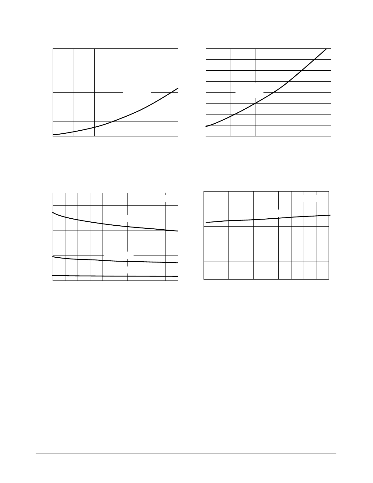
NCV4279
I
(mA)
V
(mV)
0
3.2
0
16
I
. (
A)
0
I
TYPICAL PERFORMANCE CHARACTERISTICS
14
12
10
m
D,C
8
6
4
2
0
−40 0 40 80 120 160
TJ (°C)
Figure 5. Charge Current ID,c vs. Temperature T
VI = 13.5 V
V
= 1.0 V
D
2.8
2.4
V
UD
, (V)
D
V
2.0
1.6
1.2
0.8
V
LD
0.4
0
−40 0 40 80 120 16
TJ (°C)
J
Figure 6. Switching Voltage VUD and VLD vs.
Temperature T
500
1.7
VI = 13.5 V
J
1.6
400
300
TJ = 125°C
TJ = 25°C
, (V)
1.5
1.4
1.3
DR
200
TJ = −40°C
100
DRADJ,TH
1.2
V
1.1
1.0
0
0
30 60 90 120 150 180
IQ (mA)
Figure 7. Drop Voltage VDR vs. Output Current I
35
30
25
RL = 33 W
20
q
15
10
5
RL = 50 W
RL = 100 W
0
0
10 20 30 40 50
VI (V)
Figure 9. Current Consumption Iq vs.
Input Voltage V
I
RL = 200 W
0.9
−40 0 40 80 120 16
TJ (°C)
Q
Figure 8. Reset Adjust Switching Threshold
V
RADJ,TH
vs. Temperature T
J
12
10
8
, (V)
Q
V
6
RL = 50 W
4
2
0
024681
VI (V)
Figure 10. Output Voltage VQ vs.
Input Voltage V
http://onsemi.com
7
Page 8

NCV4279
TYPICAL PERFORMANCE CHARACTERISTICS
1.6
VI = 13.5 V
1.5
1.4
, (V)
1.3
SI
V
1.2
1.1
1.0
−40 0 40 80 120 160
Sense Output High
Sense Output Low
TJ (°C)
Figure 11. Sense Threshold VSI vs. Temperature T
350
300
250
TJ = 25°C
200
(mV)
Q
150
I
TJ = 125°C
5.2
VI = 13.5 V
2.1
5.0
, (V)
4.9
Q
V
4.8
4.7
4.6
−40 0 40 80 120 160
TJ (°C)
J
Figure 12. Output Voltage VQ vs. Temperature T
J
100
50
0
0
10 20 30 40 50
VI (V)
Figure 13. Output Current IQ vs. Input Voltage V
I
http://onsemi.com
8
Page 9
NCV4279
TYPICAL PERFORMANCE CHARACTERISTICS
12
10
8
6
, (mA)
q
I
VI = 13.5 V
= 25°C
T
J
4
2
0
0 20406080100120
IQ (mA)
Figure 14. Current Consumption Iq vs.
7
6
5
4
, (mA)
q
I
3
2
1
Output Current I
IQ = 100 mA
IQ = 50 mA
IQ = 10 mA
Q
TJ = 25°C TJ = 25°C
1.6
1.4
1.2
1.0
VI = 13.5 V
0.8
, (mA)
q
I
T
= 25°C
J
0.6
0.4
0.2
0
01020304050
(mA)
I
Q
Figure 15. Current Consumption Iq vs.
, (mA)
q
I
250
200
150
100
50
Output Current I
IQ = 100 mA
Q
0
8 1012 14161820222426
6
(V)
V
I
Figure 16. Current Consumption Iq vs.
Input Voltage V
I
0
8 1012 14161820222426
6
(V)
V
I
Figure 17. Current Consumption Iq vs.
Input Voltage V
I
http://onsemi.com
9
Page 10

NCV4279
APPLICATION DESCRIPTION
OUTPUT REGULATOR
The output is controlled by a precision trimmed reference.
The PNP output has drive quiescent current control for
regulation while the input voltage is low, preventing over
saturation. Current limit and voltage monitors complement
the regulator design to give safe operating signals to the
processor and control circuits.
RESET OUTPUT (RO)
A reset signal, Reset Output, RO, (low voltage) is
generated as the IC powers up. After the output voltage V
increases above the reset threshold voltage VRT, the delay
timer D is started. When the voltage on the delay timer V
passes VUD, the reset signal RO goes high. A discharge of
the delay timer V
the reset threshold voltage V
delay timer V
is started when VQ drops and stays below
D
. When the voltage of the
RT
drops below the lower threshold voltage V
D
LD
the reset output voltage VRO is brought low to reset the
processor.
The reset output RO is an open collector NPN transistor,
controlled by a low voltage detection circuit. The circuit is
functionally independent of the rest of the IC, thereby
guaranteeing that RO is valid for V
RESET ADJUST (R
ADJ
)
as low as 1.0 V.
Q
The reset threshold VRT can be decreased from a typical
value of 4.65 V to as low as 3.5 V by using an external
voltage divider connected from the Q lead to the pin RADJ,
as shown in Figure 18. The resistor divider keeps the voltage
above the V
RADJ,TH
(typical 1.35 V) for the desired input
voltages, and overrides the internal threshold detector.
Adjust the voltage divider according to the following
relationship:
VRT+ V
RADJ,TH
@ (R
ADJ1
) R
ADJ2
)ń R
ADJ2
(eq. 1)
If the reset adjust option is not needed, the R
should be connected to GND causing the reset threshold to
go to its default value (typically 4.65 V).
RESET DELAY (D)
The reset delay circuit provides a delay (programmable by
capacitor C
provides charge current I
delay capacitor C
) on the reset output lead RO. The delay lead D
D
(typically 6.5 mA) to the external
D
during the following times:
D
1. During Powerup (once the regulation threshold has
Q
been exceeded).
2. After a reset event has occurred and the device is
D
back in regulation. The delay capacitor is set to
discharge when the regulation (V
RT
threshold voltage) has been violated. When the
delay capacitor discharges to V
, the reset signal
LD
RO pulls low.
SETTING THE DELAY TIME
The delay time is set by the delay capacitor CD and the
charge current I
. The time is measured by the delay
D
capacitor voltage charging from the low level of V
the higher level V
. The time delay follows the equation:
UD
td+ [CD(VUD* V
DSAT
)]ńI
Example:
Using C
Use the typical value for V
Use the typical value for V
= 100 nF.
D
DSAT
= 1.8 V.
UD
= 0.1 V.
Use the typical value for Delay Charge Current I
td+ [100 nF(1.8* 0.1 V)]ń 6.5 mA + 26.2 ms
, reset
D
ADJ
DSAT
(eq. 2)
= 6.5 mA.
D
(eq. 3)
pin
to
V
BAT
CI*
C
D
0.1 mF
I
D
NCV4279
Q
R
ADJ1
R
ADJ
R
ADJ2
SI
R
SI1
R
RO
R
SI2
CQ**
10 mF
R
SO
V
DD
Microprocessor
SO
required if regulator is located far from the power supply filter.
*C
I
required for Stability. Cap must operate at minimum temperature expected.
** C
Q
GND
RO
Figure 18. Application Diagram
http://onsemi.com
10
I/O
I/O
Page 11

NCV4279
V
V
SENSE INPUT (SI) / SENSE OUTPUT (SO) VOLTAGE
MONITOR
An on−chip comparator is available to provide early
warning to the microprocessor of a possible reset signal. The
output is from an open collector driver. The reset signal
typically turns the microprocessor off instantaneously. This
can cause unpredictable results with the microprocessor.
The signal received from the SO pin will allow the
microprocessor time to complete its present task before
shutting down. This function is performed by a comparator
referenced to the band gap voltage. The actual trip point can
be programmed externally using a resistor divider to the
input monitor SI (Figure 18). The values for R
SI1
and R
SI2
are selected for a typical threshold of 1.20 V on the SI Pin.
SIGNAL OUTPUT
Figure 19 shows the SO Monitor timing waveforms as a
result of the circuit depicted in Figure 18. As the output
voltage (V
) falls, the monitor threshold (V
Q
SILOW
), is
crossed. This causes the voltage on the SO output to go low
sending a warning signal to the microprocessor that a reset
signal may occur in a short period of time. T
WARNING
is the
time the microprocessor has to complete the function it is
currently working on and get ready for the reset
shutdown signal.
Q
SI
SILOW
V
RO
expensive solution, but, if the circuit operates at low
temperatures (−25°C to −40°C), both the value and ESR of
the capacitor will vary considerably. The capacitor
manufacturer’s data sheet usually provides this information.
The value for the output capacitor C
shown in Figure 18
Q
should work for most applications; however, it is not
necessarily the optimized solution. Stability is guaranteed at
values CQ = 10 mF and an ESR = 10 W within the operating
temperature range. Actual limits are shown in a graph in the
typical data section.
CALCULATING POWER DISSIPATION IN A SINGLE
OUTPUT LINEAR REGULATOR
The maximum power dissipation for a single output
regulator (Figure 18) is:
P
D(max)
+ [V
I(max)
* V
Q(min)]IQ(max)
) V
I(max)Iq
(eq. 4)
where:
V
is the maximum input voltage,
I(max)
V
I
and I
I
permissible value of R
is the minimum output voltage,
Q(min)
is the maximum output current for the application,
Q(max)
is the quiescent current the regulator consumes at
q
.
Q(max)
Once the value of P
q
= (150°C – TA) / P
R
q
JA
The value of R
can then be compared with those in the
JA
q
JA
is known, the maximum
D(max)
can be calculated:
D
(eq. 5)
package section of the data sheet. Those packages with
’s less than the calculated value in equation 2 will keep
R
JA
q
the die temperature below 150°C. In some cases, none of the
packages will be sufficient to dissipate the heat generated by
the IC, and an external heatsink will be required. The current
flow and voltages are shown in the
Measurement Circuit Diagram.
HEATSINKS
SO
A heatsink effectively increases the surface area of the
package to improve the flow of heat away from the IC and
into the surrounding air.
Each material in the heat flow path between the IC and the
T
WARNING
Figure 19. SO Warning Waveform Time Diagram
STABILITY CONSIDERATIONS
The input capacitor CI in Figure 18 is necessary for
compensating input line reactance. Possible oscillations
caused by input inductance and input capacitance can be
damped by using a resistor of approximately 1.0 W in series
with C
I.
The output or compensation capacitor helps determine
three main characteristics of a linear regulator: startup delay ,
load transient response and loop stability.
The capacitor value and type should be based on cost,
availability, size and temperature constraints. A tantalum or
aluminum electrolytic capacitor is best, since a film or
ceramic capacitor with almost zero ESR can cause
outside environment will have a thermal resistance. Like
series electrical resistances, these resistances are summed to
determine the value of R
R
+ R
qJA
JA
q
qJC
:
) R
qCS
) R
qSA
(eq. 6)
where:
= the junction−to−case thermal resistance,
R
JC
q
= the case−to−heat sink thermal resistance, and
R
CS
q
= the heat sink−to−ambient thermal resistance.
R
SA
q
appears in the package section of the data sheet. Like
R
JC
q
, it too is a function of package type. R
R
JA
q
q
CS
and R
are
SA
q
functions of the package type, heatsink and the interface
between them. These values appear in data sheets of
heatsink manufacturers. Thermal, mounting, and
heatsinking considerations are discussed in the
ON Semiconductor application note AN1040/D, available
on the ON Semiconductor website.
instability. The aluminum electrolytic capacitor is the least
http://onsemi.com
11
Page 12

NCV4279
ORDERING INFORMATION
Device Output Voltage Package Shipping
NCV4279D1
NCV4279D1G SO−8
NCV4279D1R2 SO−8
NCV4279D1R2G SO−8
NCV4279D2 SO−14
NCV4279D2G SO−14
NCV4279D2R2 SO−14
NCV4279D2R2G
†For information on tape and reel specifications,including part orientation and tape sizes, please refer to our Tape and Reel Packaging
Specifications Brochure, BRD8011/D.
5.0 V
SO−8
(Pb−Free)
(Pb−Free)
(Pb−Free)
SO−14
(Pb−Free)
98 Units/Rail
2500 Tape & Reel
55 Units/Rail
2500 Tape & Reel
†
http://onsemi.com
12
Page 13

−Y−
−Z−
NCV4279
PACKAGE DIMENSIONS
SO−8
D SUFFIX
CASE 751−07
ISSUE AF
NOTES:
−X−
A
58
B
1
S
0.25 (0.010)
4
M
M
Y
K
G
C
SEATING
PLANE
0.10 (0.004)
H
D
0.25 (0.010) Z
M
Y
SXS
N
X 45
_
M
J
1. DIMENSIONING AND TOLERANCING PER
ANSI Y14.5M, 1982.
2. CONTROLLING DIMENSION: MILLIMETER.
3. DIMENSION A AND B DO NOT INCLUDE
MOLD PROTRUSION.
4. MAXIMUM MOLD PROTRUSION 0.15 (0.006)
PER SIDE.
5. DIMENSION D DOES NOT INCLUDE DAMBAR
PROTRUSION. ALLOWABLE DAMBAR
PROTRUSION SHALL BE 0.127 (0.005) TOTAL
IN EXCESS OF THE D DIMENSION AT
MAXIMUM MATERIAL CONDITION.
6. 751−01 THRU 751−06 ARE OBSOLETE. NEW
STANDARD IS 751−07.
MILLIMETERS
DIMAMIN MAX MIN MAX
4.80 5.00 0.189 0.197
B 3.80 4.00 0.150 0.157
C 1.35 1.75 0.053 0.069
D 0.33 0.51 0.013 0.020
G 1.27 BSC 0.050 BSC
H 0.10 0.25 0.004 0.010
J 0.19 0.25 0.007 0.010
K 0.40 1.27 0.016 0.050
M 0 8 0 8
____
N 0.25 0.50 0.010 0.020
S 5.80 6.20 0.228 0.244
INCHES
SOLDERING FOOTPRINT*
1.52
0.060
7.0
0.275
0.6
0.024
*For additional information on our Pb−Free strategy and soldering
details, please download the ON Semiconductor Soldering and
Mounting Techniques Reference Manual, SOLDERRM/D.
4.0
0.155
1.270
0.050
SCALE 6:1
mm
ǒ
inches
Ǔ
http://onsemi.com
13
Page 14

−T−
SEATING
PLANE
−A−
14 8
G
D 14 PL
0.25 (0.010) A
NCV4279
PACKAGE DIMENSIONS
SO−14
D SUFFIX
CASE 751A−03
ISSUE G
NOTES:
1. DIMENSIONING AND TOLERANCING PER ANSI
Y14.5M, 1982.
2. CONTROLLING DIMENSION: MILLIMETER.
3. DIMENSIONS A AND B DO NOT INCLUDE
MOLD PROTRUSION.
4. MAXIMUM MOLD PROTRUSION 0.15 (0.006)
−B−
P
7 PL
M
71
0.25 (0.010) B
C
R
X 45
K
M
S
B
T
S
M
_
M
F
J
PER SIDE.
5. DIMENSION D DOES NOT INCLUDE DAMBAR
PROTRUSION. ALLOWABLE DAMBAR
PROTRUSION SHALL BE 0.127 (0.005) TOTAL
IN EXCESS OF THE D DIMENSION AT
MAXIMUM MATERIAL CONDITION.
DIM MIN MAX MIN MAX
A 8.55 8.75 0.337 0.344
B 3.80 4.00 0.150 0.157
C 1.35 1.75 0.054 0.068
D 0.35 0.49 0.014 0.019
F 0.40 1.25 0.016 0.049
G 1.27 BSC 0.050 BSC
J 0.19 0.25 0.008 0.009
K 0.10 0.25 0.004 0.009
M 0 7 0 7
____
P 5.80 6.20 0.228 0.244
R 0.25 0.50 0.010 0.019
INCHESMILLIMETERS
ON Semiconductor and are registered trademarks of Semiconductor Components Industries, LLC (SCILLC). SCILLC reserves the right to make changes without further notice
to any products herein. SCILLC makes no warranty, representation or guarantee regarding the suitability of its products for any particular purpose, nor does SCILLC assume any liability
arising out of the application or use of any product or circuit, and specifically disclaims any and all liability, including without limitation special, consequential or incidental damages.
“Typical” parameters which may be provided in SCILLC data sheets and/or specifications can and do vary in different applications and actual performance may vary over time. All
operating parameters, including “Typicals” must be validated for each customer application by customer’s technical experts. SCILLC does not convey any license under its patent rights
nor the rights of others. SCILLC products are not designed, intended, or authorized for use as components in systems intended for surgical implant into the body, or other applications
intended to support or sustain life, or for any other application in which the failure of the SCILLC product could create a situation where personal injury or death may occur. Should
Buyer purchase or use SCILLC products for any such unintended or unauthorized application, Buyer shall indemnify and hold SCILLC and its officers, employees, subsidiaries, affiliates,
and distributors harmless against all claims, costs, damages, and expenses, and reasonable attorney fees arising out of, directly or indirectly, any claim of personal injury or death
associated with such unintended or unauthorized use, even if such claim alleges that SCILLC was negligent regarding the design or manufacture of the part. SCILLC is an Equal
Opportunity/Affirmative Action Employer. This literature is subject to all applicable copyright laws and is not for resale in any manner.
PUBLICATION ORDERING INFORMATION
LITERATURE FULFILLMENT:
Literature Distribution Center for ON Semiconductor
P.O. Box 61312, Phoenix, Arizona 85082−1312 USA
Phone: 480−829−7710 or 800−344−3860 Toll Free USA/Canada
Fax: 480−829−7709 or 800−344−3867 Toll Free USA/Canada
Email: orderlit@onsemi.com
N. American Technical Support: 800−282−9855 Toll Free
USA/Canada
Japan: ON Semiconductor, Japan Customer Focus Center
2−9−1 Kamimeguro, Meguro−ku, Tokyo, Japan 153−0051
Phone: 81−3−5773−3850
http://onsemi.com
ON Semiconductor Website: http://onsemi.com
Order Literature: http://www.onsemi.com/litorder
For additional information, please contact your
local Sales Representative.
NCV4279/D
14
 Loading...