

Page 1
查询NCV4275供应商
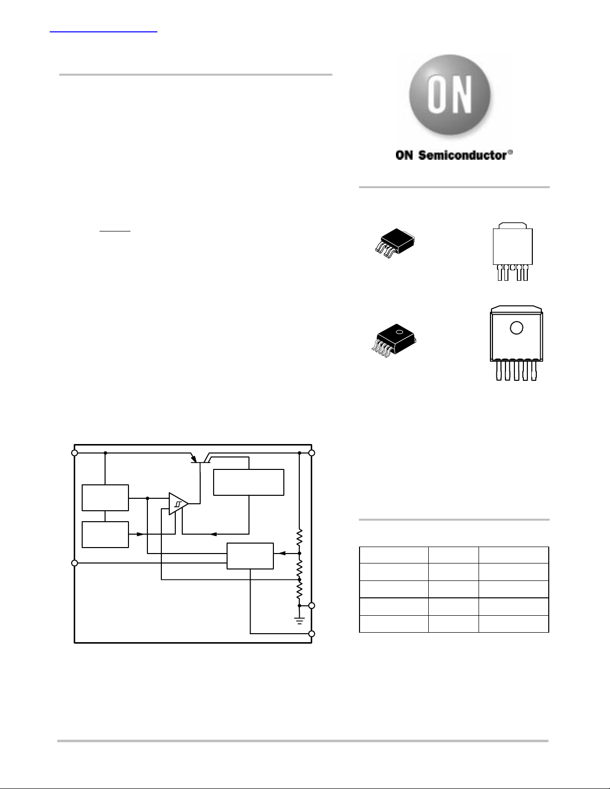
NCV4275
5.0 V Low−Drop Voltage
Regulator
This industry standard linear regulator has the capability to drive
loads up to 450 mA at 5.0 V. It is available in DPAK and D2PAK.
This device is pin−for−pin compatible with Infineon part number
TLE4275.
http://onsemi.com
http://onsemi.com
Features
• 5.0 V, ±2%, 450 mA Output Voltage
• Very Low Current Consumption
• Active RESET
• Reset Low Down to V
= 1.0 V
Q
• 500 mV (max) Dropout Voltage
• Fault Protection
♦ +45 V Peak Transient Voltage
♦ −42 V Reverse Voltage
♦ Short Circuit
♦ Thermal Overload
• NCV Prefix for Automotive and Other Applications Requiring Site
and Control Changes
I
Bandgap
Reference
Error
Amplifier
+
−
Current Li m i t a n d
Saturation Sense
Q
MARKING
DIAGRAMS
DPAK
5−PIN
1
5
1
5
DT SUFFIX
CASE 175AA
D2PAK
5−PIN
DS SUFFIX
CASE 936A
Pin 1. I
2. RO
Tab, 3. GND*
4. D
5. Q
* Tab is connected to
Pin 3 on all packages
A = Assembly Location
WL, L = Wafer Lot
YY, Y = Year
WW = Work Week
4275
ALYWW
1
NCV4275
AWLYYWW
1
x
Thermal
Shutdown
D
Figure 1. Block Diagram
Semiconductor Components Industries, LLC, 2004
August, 2004 − Rev. 8
Reset
Generator
ORDERING INFORMATION
Device Package Shipping
NCV4275DT DPAK 75 Units/Rail
NCV4275DTRK DPAK 2500 Tape & Reel
GND
RO
1 Publication Order Number:
NCV4275DS D2PAK 50 Units/Rail
NCV4275DSR4 D2PAK 800 Tape & Reel
†For information on tape and reel specifications,
including part orientation and tape sizes, please
refer to our Tape and Reel Packaging Specification
Brochure, BRD8011/D.
†
NCV4275/D
Page 2
NCV4275
СССССС
СССССС
СССССС
СССССС
СССССС
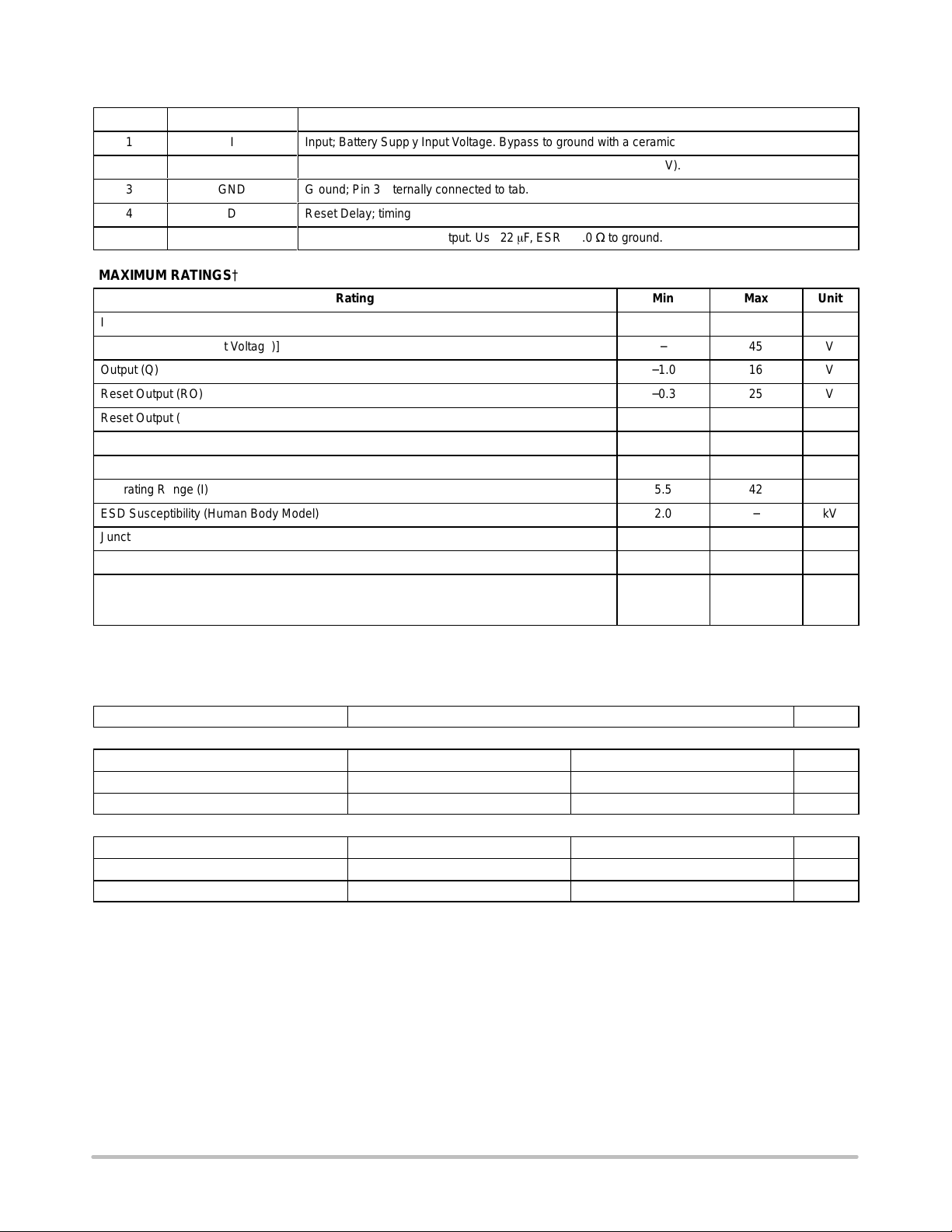
PIN FUNCTION DESCRIPTION
Pin No. Symbol Description
1
2
3
4
5
MAXIMUM RATINGS†
Input [I (DC)] −42 45 V
Input [I (Peak Transient Voltage)] − 45 V
Output (Q) −1.0 16 V
Reset Output (RO) −0.3 25 V
Reset Output (RO) −5.0 5.0 mA
Reset Delay (D) −0.3 7.0 V
Reset Delay (D) −2.0 2.0 mA
Operating Range (I) 5.5 42 V
ESD Susceptibility (Human Body Model) 2.0 − kV
Junction Temperature −40 150 °C
Storage Temperature −55 150 °C
Lead Temperature Soldering Reflow (SMD styles only) Note 1
Maximum ratings are those values beyond which device damage can occur. Maximum ratings applied to the device are individual stress limit values
(not normal operating conditions) and are not valid simultaneously. If these limits are exceeded, device functional operation is not implied, damage
may occur and reliability may be affected.
I
RO
GND
D
Q
Input; Battery Supply Input Voltage. Bypass to ground with a ceramic capacitor.
Reset Output; Open Collector Active Reset (accurate when I > 1.0 V).
Ground; Pin 3 internally connected to tab.
Reset Delay; timing capacitor to GND for Reset Delay function.
Output; ±2.0%, 450 mA output. Use 22 F, ESR < 5.0 Ω to ground.
Rating Min Max Unit
−
240 Peak
(Note 3)
Wave Solder (through hole styles only) Note 2
−
260 Peak
°C
°C
THERMAL CHARACTERISTICS
Parameter Test Conditions (Typical Value) Unit
DPAK 5−PIN PACKAGE
Min Pad Board (Note 4) 1″ Pad Board (Note 5)
Junction−to−Tab (psi−JLx,
Junction−to−Ambient (R
D2PAK 5−PIN PACKAGE
Junction−to−Tab (psi−JLx,
Junction−to−Ambient (R
1. 60 seconds max above 183°C.
2. 10 seconds max.
3. −5°C/+0°C allowable conditions.
4. 1 oz. copper, 0.26 inch2 (168 mm2) copper area, 0.62″ thick FR4.
5. 1 oz. copper, 1.14 inch2 (736 mm2) copper area, 0.62″ thick FR4.
6. 1 oz. copper, 0.373 inch2 (241 mm2) copper area, 0.62″ thick FR4.
7. 1 oz. copper, 1.222 inch2 (788 mm2) copper area, 0.62″ thick FR4.
†During the voltage range which exceeds the maximum tested voltage of I, operation is assured, but not specified. Wider limits may apply. Thermal
dissipation must be observed closely.
) 4.2 4.7 C/W
JLx
, JA) 100.9 46.8 C/W
JA
0.4 sq. in. Spreader Board (Note 6) 1.2 sq. in. Spreader Board (Note 7)
) 3.8 4.0 C/W
JLx
, JA) 74.8 41.6 C/W
JA
http://onsemi.com
2
Page 3
NCV4275
ELECTRICAL CHARACTERISTICS (I = 13.5 V; −40°C < T
< 150°C; unless otherwise noted)
J
Characteristic Test Conditions Min Typ Max Unit
Output
Output Voltage 5.0 mA < IQ < 400 mA, 6.0 V < VI < 28 V 4.9 5.0 5.1 V
Output Voltage 5.0 mA < IQ < 200 mA, 6.0 V < VI < 40 V 4.9 5.0 5.1 V
Output Current Limitation − 450 700 − mA
Quiescent Current, Iq = II − I
Quiescent Current, Iq = II − I
Quiescent Current, Iq = II − I
Q
Q
Q
Dropout Voltage IQ = 300 mA, Vdr = VI − V
IQ = 1.0 mA − 150 200 A
IQ = 250 mA − 10 15 mA
IQ = 400 mA − 23 35 mA
Q
− 250 500 mV
Load Regulation IQ = 5.0 mA to 400 mA −30 15 30 mV
Line Regulation ∆V = 8.0 V to 32 V, IQ = 5.0 mA −25 5.0 25 mV
Power Supply Ripple Rejection fr = 100 Hz, Vr = 0.5 V
pp
− 60 − dB
Temperature Output Voltage Drift − − 0.5 − mV/k
Reset Timing D and Output RO
Reset Switching Threshold − 4.5 4.65 4.8 V
Reset Output Low Voltage R
Reset Output Leakage Current V
> 5.0 k, VQ > 1.0 V − 0.2 0.4 V
ext
= 5.0 V − 0 10 A
ROH
Reset Charging Current VD = 1.0 V 3.0 5.5 9.0 A
Upper Timing Threshold − 1.5 1.8 2.2 V
Lower Timing Threshold − 0.2 0.4 0.7 V
Reset Delay Time CD = 47 nF 10 16 22 ms
Reset Reaction Time CD = 47 nF − 1.5 4.0 s
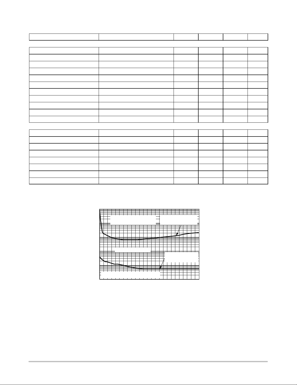
TYPICAL PERFORMANCE CHARACTERISTICS
1000
Unstable ESR Region for
C
= 1 F − 22 F
100
Vout
10
ESR ()
1
Stable ESR Region
0.1
Unstable Region for C
0.01
0 100 200 300 400 500
Vout
= 1 F
OUTPUT CURRENT (mA)
Figure 2. Output Stability with Output
Capacitor ESR
Maximum ESR for
C
= 1 F − 22 F
Vout
Minimum ESR for
C
= 1 F
Vout
http://onsemi.com
3
Page 4
NCV4275
APPLICATION INFORMATION
I
V
I
C
I1
1000 µF
I
C
I2
100 nF
I
D
C
D
47 nF
I
1
D
4
Figure 3. Test Circuit
Circuit Description
The error amplifier compares a temperature−stable
reference voltage to a voltage that is proportional to the
output voltage (Q) (generated from a resistor divider) and
drives the base of a series transistor via a buffer. Saturation
control as a function of the load current prevents
oversaturation of the output power device, thus preventing
excessive substrate current (quiescent current).
Typical drop out voltage at 300 mA load is 250 mV,
500 mV maximum. Test voltage for drop out is 5.0 V input.
Stability Considerations
The input capacitors (CI1 and CI2) are necessary to
control line influences. Using a resistor of approximately
1.0 Ω in series with CI2 can solve potential oscillations due
to stray inductance and capacitance.
The output or compensation capacitor helps determine
three main characteristics of a linear regulator: start−up
delay, load transient response and loop stability.
The capacitor value and type should be based on cost,
availability, size and temperature constraints. A tantalum
or aluminum electrolytic capacitor is best, since a film or
ceramic capacitor with almost zero ESR can cause
instability. The aluminum electrolytic capacitor is the least
expensive solution, but, if the circuit operates at low
temperatures (−25°C to −40°C), both the value and ESR of
the capacitor will vary considerably. The capacitor
manufacturers data sheet usually provides this
information.
The value for the output capac itor CQ shown in Figure 3
should work for most applications, however it is not
necessarily the op timized solution. Stability is guaranteed for
CQ > 22 F and an ESR ≤ 5.0 Ω.
I
C
Q
22 µF
Q
R
ext
5.0 k
NCV4275
3
GND
Q
5
I
RO
2
RO
Calculating Power Dissipation
in a Single Output Linear Regulator
The maximum power dissipation for a single output
regulator (Figure 4) is:
P
D(max)
[V
V
I(max)
I(max)Iq
V
Q(min)]IQ(max)
where
V
I(max)
V
Q(min)
I
Q(max)
is the maximum input voltage,
is the minimum output voltage,
is the maximum output current for the
application,
Iq is the quiescent current the regulator
consumes at I
Once the value of P
permissible value of R
R
JA
The value of R
can then be compared with those in the
JA
D(max)
can be calculated:
JA
150°C
.
Q(max)
is known, the maximum
T
A
P
D
package section of the data sheet. Those packages with
R
’s less than the calculated value in Equation 2 will keep
JA
the die temperature below 150°C.
In some cases, none of the packages will be sufficient to
dissipate the heat generated by the IC, and an external
heatsink will be required.
I
I
V
I
SMART
REGULATOR
Control
}
Features
Iq
I
Q
V
Q
V
RO
(1)
(2)
V
Q
http://onsemi.com
4
Figure 4. Single Output Regulator with Key
Performance Parameters Labeled
Page 5

NCV4275
Heat Sinks
A heat sink effectively increases the surface area of the
package to improve the flow of heat away from the IC and
into the surrounding air.
Each material in the heat flow path between the IC and
the outside environment will have a thermal resistance.
Like series electrical resistances, these resistances are
summed to determine the value of R
R
R
JA
V
I
V
Q
JC
R
CS
R
JA
:
SA
(3)
where
R
is the junction−to−case thermal resistance,
JC
R
is the case−to−heatsink thermal resistance,
CS
R
is the heatsink−to−ambient thermal
SA
resistance.
R
appears in the package section of the data sheet.
JC
Like R
R
SA
, it too is a function of package type. R
JA
and
CS
are functions of the package type, heatsink and the
interface between them. These values appear in heat sink
data sheets of heat sink manufacturers.
Thermal, mounting, and heatsinking considerations are
discussed in the ON Semiconductor application note
AN1040/D.
t
< Reset Reaction Time
V
Q,rt
V
D
Reset
Delay Time
V
RO
Power−on−Reset Thermal
Reset
Reaction Time
Shutdown
Voltage Dip
at Input
Undervoltage Secondary
Figure 5. Reset Timing
Spike
Reset Charge Current
dV
D
dt
Overload
at Output
t
C
D
Upper Timing Threshold
Lower Timing Threshold
t
t
http://onsemi.com
5
Page 6

NCV4275
Table 1. DPAK 5−Lead Thermal RC Network Models
Drain Copper Area (1 oz thick) 168 mm
2
(SPICE Deck Format) Cauer Network Foster Network
2
168 mm
C_C1 Junction Gnd 1.00E−06 1.00E−06 W−s/C 1.36E−08 1.361E−08 sec
C_C2 node1 Gnd 1.00E−05 1.00E−05 W−s/C 7.41E−07 7.411E−07 sec
C_C3 node2 Gnd 6.00E−05 6.00E−05 W−s/C 1.04E−05 1.029E−05 sec
C_C4 node3 Gnd 1.00E−04 1.00E−04 W−s/C 3.91E−05 3.737E−05 sec
C_C5 node4 Gnd 4.36E−04 3.64E−04 W−s/C 1.80E−03 1.376E−03 sec
C_C6 node5 Gnd 6.77E−02 1.92E−02 W−s/C 3.77E−01 2.851E−02 sec
C_C7 node6 Gnd 1.51E−01 1.27E−01 W−s/C 3.79E+00 9.475E−01 sec
C_C8 node7 Gnd 4.80E−01 1.018 W−s/C 2.65E+01 1.173E+01 sec
C_C9 node8 Gnd 3.740 2.955 W−s/C 8.71E+01 8.59E+01 sec
C_C10 node9 Gnd 10.322 0.438 W−s/C sec
2
168 mm
R_R1 Junction node1 0.015 0.015 C/W 0.0123 0.0123 C/W
R_R2 node1 node2 0.08 0.08 C/W 0.0585 0.0585 C/W
R_R3 node2 node3 0.4 0.4 C/W 0.0304 0.0287 C/W
R_R4 node3 node4 0.2 0.2 C/W 0.3997 0.3772 C/W
R_R5 node4 node5 2.97519 2.6171 C/W 3.115 2.68 C/W
R_R6 node5 node6 8.2971 1.6778 C/W 3.571 1.38 C/W
R_R7 node6 node7 25.9805 7.4246 C/W 12.851 5.92 C/W
R_R8 node7 node8 46.5192 14.9320 C/W 35.471 7.39 C/W
R_R9 node8 node9 17.7808 19.2560 C/W 46.741 28.94 C/W
R_R10 node9 Gnd 0.1 0.1758 C/W C/W
NOTE: Bold face items represent the package without the external thermal system.
736 mm
736 mm
736 mm
2
2
2
Units Tau Tau Units
2
168 mm
R’s R’s
736 mm
2
http://onsemi.com
6
Page 7

NCV4275
T able 2 . D2P AK 5−Lead Thermal RC Network Models
241 mm
241 mm
2
2
2
Drain Copper Area (1 oz thick) 241 mm
(SPICE Deck Format) Cauer Network Foster Network
C_C1 Junction Gnd 1.00E−06 1.00E−06 W−s/C 1.361E−08 1.361E−08 sec
C_C2 node1 Gnd 1.00E−05 1.00E−05 W−s/C 7.411E−07 7.411E−07 sec
C_C3 node2 Gnd 6.00E−05 6.00E−05 W−s/C 1.005E−05 1.007E−05 sec
C_C4 node3 Gnd 1.00E−04 1.00E−04 W−s/C 3.460E−05 3.480E−05 sec
C_C5 node4 Gnd 2.82E−04 2.87E−04 W−s/C 7.868E−04 8.107E−04 sec
C_C6 node5 Gnd 5.58E−03 5.95E−03 W−s/C 7.431E−03 7.830E−03 sec
C_C7 node6 Gnd 4.25E−01 4.61E−01 W−s/C 2.786E+00 2.012E+00 sec
C_C8 node7 Gnd 9.22E−01 2.05 W−s/C 2.014E+01 2.601E+01 sec
C_C9 node8 Gnd 1.73 4.88 W−s/C 1.134E+02 1.218E+02 sec
C_C10 node9 Gnd 7.12 1.31 W−s/C sec
R_R1 Junction node1 0.015 0.0150 C/W 0.0123 0.0123 C/W
R_R2 node1 node2 0.08 0.0800 C/W 0.0585 0.0585 C/W
R_R3 node2 node3 0.4 0.4000 C/W 0.0257 0.0260 C/W
R_R4 node3 node4 0.2 0.2000 C/W 0.3413 0.3438 C/W
R_R5 node4 node5 1.85638 1.8839 C/W 1.77 1.81 C/W
R_R6 node5 node6 1.23672 1.2272 C/W 1.54 1.52 C/W
R_R7 node6 node7 9.81541 5.3383 C/W 4.13 3.46 C/W
R_R8 node7 node8 33.1868 18.9591 C/W 6.27 5.03 C/W
R_R9 node8 node9 27.0263 13.3369 C/W 60.80 29.30 C/W
R_R10 node9 gnd 1.13944 0.1191 C/W C/W
NOTE: Bold face items represent the package without the external thermal system.
788 mm
653 mm
653 mm
2
2
2
Units Tau Tau Units
2
241 mm
R’s R’s
788 mm
2
The Cauer networks generally have physical significance and may be divided between nodes to separate thermal behavior
due to one portion of the network from another. The Foster networks, though when sorted by time constant (as above) bear
a rough correlation with the Cauer networks, are really only convenient mathematical models. Cauer networks can be easily
implemented using circuit simulating tools, whereas Foster networks may be more easily implemented using mathematical
tools (for instance, in a spreadsheet program), according to the following formula:
n
R(t)
i 1
http://onsemi.com
−ttau
R
1−e
i
7
i
Page 8

NCV4275
110
100
JA (C°/W)
90
80
70
60
50
40
30
150
2 oz
200 250 300 350 400 450 500 550 600 650 700 750
1 oz
COPPER AREA (mm2)
Figure 6. JA vs. Copper Spreader Area,
DPAK 5−Lead
100
10
110
100
JA (C°/W)
90
80
70
60
50
40
30
150
2 oz
200 250 300 350 400 450 500 550 600 650 700 750
1 oz
COPPER AREA (mm2)
Figure 7. JA vs. Copper Spreader Area,
2
P AK 5−Lead
D
Cu Area 167 mm
2
Cu Area 736 mm
2
1.0
R(t) C°/W
sqrt(t)
0.1
0.01
0.0000001 0.000001 0.00001 0.0001 0.001 0.01 0.1 1.0 10 100 1000
TIME (sec)
Figure 8. Single−Pulse Heating Curves, DPAK 5−Lead
100
Cu Area 167 mm
10
1.0
R(t) C°/W
0.1
0.01
0.0000001 0.000001 0.00001 0.0001 0.001 0.01 0.1 1.0 10 100 1000
TIME (sec)
2
Cu Area 736 mm
2
Figure 9. Single−Pulse Heating Curves, D2P AK 5−Lead
http://onsemi.com
8
Page 9

NCV4275
100
50% Duty Cycle
20%
10
10%
1.0
0.1
10
1.0
0.1
5%
2%
1%
Non−normalized Response
PULSE WIDTH (sec)
Figure 10. Duty Cycle for 1” Spreader Boards, DPAK 5−Lead
50% Duty Cycle
20%
10%
5%
2%
1%
C°/W
2
736 mm
JA
R
0.01
0.0000001 0.000001 0.00001 0.0001 0.001 0.01 0.1 1.0 10 100 1000
100
C°/W
2
788 mm
JA
R
Non−normalized Response
0.01
0.0000001 0.000001 0.00001 0.0001 0.001 0.01 0.1 1.0 10 100 1000
PULSE WIDTH (sec)
Figure 11. Duty Cycle for 1” Spreader Boards, D2P AK 5−Lead
Junction
Time constants are
R
1
C
1
not
of mathematical solution are
R
2
C
2
R
3
C
3
simple RC products. Amplitudes
not
the resistance values.
R
n
C
n
Ambient
(thermal ground)
Figure 12. Grounded Capacitor Thermal Network (“Cauer” Ladder)
Junction
R
1
C
1
R
2
C
2
R
3
C
3
R
n
C
n
Each rung is exactly characterized by its RC−product
time constant; amplitudes are the resistances.
Ambient
(thermal ground)
Figure 13. Non−Grounded Capacitor Thermal Ladder (“Foster” Ladder)
http://onsemi.com
9
Page 10

NCV4275
PACKAGE DIMENSIONS
DPAK 5 CENTER LEAD CROP
DT SUFFIX
CASE 175AA−01
ISSUE O
NOTES:
1. DIMENSIONING AND TOLERANCING
SEATING
−T−
PLANE
B
V
S
R
A
123 4 5
K
F
L
D
5 PL
G
0.13 (0.005) T
C
E
R1
Z
U
J
H
M
PER ANSI Y14.5M, 1982.
2. CONTROLLING DIMENSION: INCH.
DIM MIN MAX MIN MAX
A 0.235 0.245 5.97 6.22
B 0.250 0.265 6.35 6.73
C 0.086 0.094 2.19 2.38
D 0.020 0.028 0.51 0.71
E 0.018 0.023 0.46 0.58
F 0.024 0.032 0.61 0.81
G 0.180 BSC 4.56 BSC
H 0.034 0.040 0.87 1.01
J 0.018 0.023 0.46 0.58
K 0.102 0.114 2.60 2.89
L 0.045 BSC 1.14 BSC
R 0.170 0.190 4.32 4.83
R1 0.185 0.210 4.70 5.33
S 0.025 0.040 0.63 1.01
U 0.020 −−− 0.51 −−−
V 0.035 0.050 0.89 1.27
Z 0.155 0.170 3.93 4.32
MILLIMETERSINCHES
http://onsemi.com
10
Page 11

K
B
D
0.010 (0.254) T
M
C
A
123
45
G
S
H
OPTIONAL
CHAMFER
NCV4275
PACKAGE DIMENSIONS
D2PAK
5 LEAD
DS SUFFIX
CASE 936A−02
ISSUE B
−T−
E
M
N
R
TERMINAL 6
V
L
P
NOTES:
1. DIMENSIONING AND TOLERANCING PER ANSI
Y14.5M, 1982.
2. CONTROLLING DIMENSION: INCH.
3. TAB CONTOUR OPTIONAL WITHIN DIMENSIONS
U
A AND K.
4. DIMENSIONS U AND V ESTABLISH A MINIMUM
MOUNTING SURFACE FOR TERMINAL 6.
5. DIMENSIONS A AND B DO NOT INCLUDE MOLD
FLASH OR GATE PROTRUSIONS. MOLD FLASH
AND GATE PROTRUSIONS NOT TO EXCEED
0.025 (0.635) MAXIMUM.
INCHES
DIMAMIN MAX MIN MAX
0.386 0.403 9.804 10.236
B 0.356 0.368 9.042 9.347
C 0.170 0.180 4.318 4.572
D 0.026 0.036 0.660 0.914
E 0.045 0.055 1.143 1.397
G 0.067 BSC 1.702 BSC
H 0.539 0.579 13.691 14.707
K 0.050 REF 1.270 REF
L 0.000 0.010 0.000 0.254
M 0.088 0.102 2.235 2.591
N 0.018 0.026 0.457 0.660
P 0.058 0.078 1.473 1.981
R 5 REF
S 0.116 REF 2.946 REF
U 0.200 MIN 5.080 MIN
V 0.250 MIN 6.350 MIN
MILLIMETERS
5 REF
http://onsemi.com
11
Page 12

NCV4275
ON Semiconductor and are registered trademarks of Semiconductor Components Industries, LLC (SCILLC). SCILLC reserves the right to make changes without further notice
to any products herein. SCILLC makes no warranty, representation or guarantee regarding the suitability of its products for any particular purpose, nor does SCILLC assume any
liability arising out of the application or use of any product or circuit, and specifically disclaims any and all liability, including without limitation special, consequential or incidental
damages. “Typical” parameters which may be provided in SCILLC data sheets and/or specifications can and do vary in different applications and actual performance may vary over
time. All operating parameters, including “Typicals” must be validated for each customer application by customer’s technical experts. SCILLC does not convey any license under
its patent rights nor the rights of others. SCILLC products are not designed, intended, or authorized for use as components in systems intended for surgical implant into the body,
or other applications intended to support or sustain life, or for any other application in which the failure of the SCILLC product could create a situation where personal injury or death
may occur. Should Buyer purchase or use SCILLC products for any such unintended or unauthorized application, Buyer shall indemnify and hold SCILLC and its officers, employees,
subsidiaries, affiliates, and distributors harmless against all claims, costs, damages, and expenses, and reasonable attorney fees arising out of, directly or indirectly, any claim of
personal injury or death associated with such unintended or unauthorized use, even if such claim alleges that SCILLC was negligent regarding the design or manufacture of the part.
SCILLC is an Equal Opportunity/Affirmative Action Employer. This literature is subject to all applicable copyright laws and is not for resale in any manner.
PUBLICATION ORDERING INFORMATION
LITERATURE FULFILLMENT:
Literature Distribution Center for ON Semiconductor
P.O. Box 61312, Phoenix, Arizona 85082−1312 USA
Phone: 480−829−7710 or 800−344−3860 Toll Free USA/Canada
Fax: 480−829−7709 or 800−344−3867 Toll Free USA/Canada
Email: orderlit@onsemi.com
N. American Technical Support: 800−282−9855 Toll Free
USA/Canada
Japan: ON Semiconductor, Japan Customer Focus Center
2−9−1 Kamimeguro, Meguro−ku, Tokyo, Japan 153−0051
Phone: 81−3−5773−3850
http://onsemi.com
ON Semiconductor Website: http://onsemi.com
Order Literature: http://www.onsemi.com/litorder
For additional information, please contact your
local Sales Representative.
NCV4275/D
12
 Loading...