

查询NCV1009D供应商
NCV1009
2.5 Volt Reference
The NCV1009 is a precision trimmed 2.5 V ±5.0 mV shunt
regulator diode. The low dynamic impedance and wide operating
current range enhances its versatility. The tight reference tolerance is
achieved by on−chip trimming which minimizes voltage tolerance and
temperature drift.
A third terminal allows the reference voltage to be adjusted ±5.0%
to calibrate out system errors. In many applications, the NCV1009Z
can be used as a pin−to−pin replacement of the LT1009CZ and the
LM136Z−2.5 with the external trim network eliminated.
Features
• 0.2% Initial Tolerance Max.
• Guaranteed Temperature Stability
• Maximum 0.6 Ω Dynamic Impedance
• Wide Operating Current Range
• Directly Interchangeable with LT1009 and LM136 for Improved
Performance
• No Adjustments Needed for Minimum Temperature Coefficient
• Meets Mil Std 883C ESD Requirements
• Extended Operating Temperature Range for Use in Automotive
Applications
• NCV Prefix, for Automotive and Other Applications Requiring Site
and Change Control
http://onsemi.com
http://onsemi.com
AYWW
1009D
D SUFFIX
CASE 751
8
1
PIN CONNECTIONS AND
MARKING DIAGRAM
1
NC
A = Assembly Location
Y = Year
WW = Work Week
SO−8
8
NCNC
NCNC
V
REF
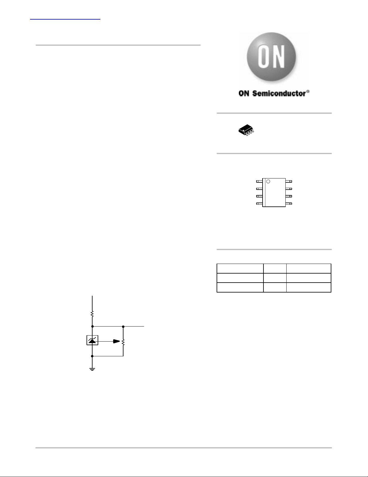
ADJ. PINGND
5.0 V−35 V
3.6 kΩ
V
REF
ADJ
GND
*±5.0% Trim Range
If the external trim resistor is not used, the “ADJ. PIN” should
be left floating. The 10k trim potentiometer does not effect the
temperature coefficient of the device.
Figure 1. Application Diagram
10 kΩ∗
TRIM
ORDERING INFORMATION
Device Package Shipping
NCV1009D
NCV1009DR2
†For information on tape and reel specifications,
including part orientation and tape sizes, please
refer to our Tape and Reel Packaging Specification
Brochure, BRD8011/D.
SO−8
SO−8
95 Units/Rail
2500 Tape & Reel
†
Semiconductor Components Industries, LLC, 2004
August, 2004 − Rev. 6
1 Publication Order Number:
NCV1009/D
V
REF
NCV1009
N1
15 pF
N2
14 kΩ
P1
N3
20 pF
N6N5
SUBSTRATE
10 pF
P2
N4
P3
63 kΩ
N7
N9
1.14 kΩ
GND
Figure 2. Block Diagram
N8
N10
N12 N13
1.14 kΩ
TRIM
20 kΩ
N14
N11
N16
20 kΩ
10.15 kΩ
30 kΩ
ADJ
6.785 kΩ
D1
N15
http://onsemi.com
2

NCV1009
MAXIMUM RATINGS*
Rating Value Unit
Reverse Current 20 mA
Forward 10 mA
Package Thermal Resistance, SO−8:
Junction−to−Case, R
Junction−to−Ambient, R
θ
JC
θ
JA
Operating Temperature Range −40 to +125 °C
Storage Temperature Range −65 to +150 °C
Lead Temperature Soldering: Wave Solder (through hole styles only) (Note 1)
Reflow: (SMD styles only) (Notes 2, 3)
Maximum ratings are those values beyond which device damage can occur. Maximum ratings applied to the device are individual stress limit
values (not normal operating conditions) and are not valid simultaneously . If these limits are exceeded, device functional operation is not implied,
damage may occur and reliability may be affected.
1. 10 second maximum
2. 60 second maximum above 183°C.
3. −5°C / +0°C allowable conditions.
*The maximum package power dissipation must be observed.
45
165
260 peak
240 peak
°C/W
°C/W
°C
°C
ELECTRICAL CHARACTERISTICS (T
Characteristic
Reverse Breakdown Voltage I
= 25°C unless otherwise specified.)
A
Test Conditions Min Typ Max Unit
= 1.0 mA 2.492 2.500 2.508 V
R
Reverse Breakdown Voltage 0°C ≤ TA ≤ 125°C 2.492 2.500 2.508 V
Reverse Breakdown Voltage −40°C ≤TA≤ 0°C 2.480 2.500 2.508 V
Reverse Breakdown Voltage
Change with Current
Reverse Dynamic Impedance I
Temperature Stability
Average Temperature Coefficient
Long Term Stabilty T
400 µA ≤ I
= 1.0 mA
R
0°C ≤ TA ≤ 70°C, Note 4
0°C ≤ T
= 25°C ±0.1 C, IR = 1.0 mA − 20 − ppm/kHr
A
≤ 10 mA
R
≤ 70°C, Note 4
A
−
−
−
−
−
−
2.6
3.0
0.2
0.4
1.8
15
5.0
6.0
1.0
1.4
−
−
† Denotes the specifications which apply over full operating temperature range.
4. Average temperature coefficient is defined as the total voltage change divided by the specified temperature range.
TYPICAL PERFORMANCE CHARACTERISTICS
10
10
−1
−2
5
4
mV
mV
Ω
Ω
mV
ppm/°C
−3
10
−4
10
REVERSE CURRENT (A)
T
= 25°C
J
−5
10
0.5
1.0
1.4 1.8
REVERSE VOLTAGE (V)
Figure 3. Reverse Current vs. Reverse Voltage
2.2
2.6
http://onsemi.com
3
2
1
REVERSE VOLTAGE CHANGE (mV)
0
0
3
4
812
16
REVERSE CURRENT (mA)
Figure 4. Change in Reverse Voltage vs.
Reverse Current
20

NCV1009
()
1.2
TJ = 25°C
1.0
0.8
0.6
0.4
FORWARD VOLTAGE (V)
0.2
0
0.001
0.01 0.1 1.0 10
Figure 5. Forward Voltage vs. Forward Current
250
IR = ImA
TJ = 25°C
200
150
NOISE (nV/√HZ)
100
50
10 100 1.0 k 10 k 100 k
FREQUENCY (Hz)
Figure 7. Zener Noise Voltage vs. Frequency Figure 8. Response Time
100
10
1.0
DYNAMIC IMPEDANCE (Ω)
0.1
10
Figure 6. Dynamic Impedance vs. Frequency
0
2.5
2.0
1.5
1.0
0.5
0
VOLTAGE SWING (V)
10.010.0
4.0
0
0
100 1.0 k 10 k 100 k
FREQUENCY (Hz)FORWARD CURRENT (mA)
5.0 k
INPUT
OUTPUT
120
TIME (µs)
2.520
2.510
2.500
2.490
REFERENCE VOLTAGE (V)
−40
−30 0 25 35 70 105
Figure 9. Reference Voltage vs. Temperature
http://onsemi.com
4

−Y−
−Z−
NCV1009
PACKAGE DIMENSIONS
SO−8
D SUFFIX
CASE 751−07
ISSUE AC
NOTES:
−X−
A
58
B
1
S
0.25 (0.010)
4
M
M
Y
K
G
C
SEATING
PLANE
0.10 (0.004)
H
D
0.25 (0.010) Z
M
Y
SXS
N
X 45
M
1. DIMENSIONING AND TOLERANCING PER ANSI
Y14.5M, 1982.
2. CONTROLLING DIMENSION: MILLIMETER.
3. DIMENSION A AND B DO NOT INCLUDE MOLD
PROTRUSION.
4. MAXIMUM MOLD PROTRUSION 0.15 (0.006) PER
SIDE.
5. DIMENSION D DOES NOT INCLUDE DAMBAR
PROTRUSION. ALLOWABLE DAMBAR
PROTRUSION SHALL BE 0.127 (0.005) TOTAL IN
EXCESS OF THE D DIMENSION AT MAXIMUM
MATERIAL CONDITION.
6. 751−01 THRU 751−06 ARE OBSOLETE. NEW
STANDARD IS 751−07
MILLIMETERS
DIMAMIN MAX MIN MAX
4.80 5.00 0.189 0.197
B 3.80 4.00 0.150 0.157
C 1.35 1.75 0.053 0.069
D 0.33 0.51 0.013 0.020
G 1.27 BSC 0.050 BSC
H 0.10 0.25 0.004 0.010
J
J 0.19 0.25 0.007 0.010
K 0.40 1.27 0.016 0.050
M 0 8 0 8
N 0.25 0.50 0.010 0.020
S 5.80 6.20 0.228 0.244
INCHES
SOLDERING FOOTPRINT
7.0
0.275
0.6
0.024
1.52
0.060
4.0
0.155
1.270
0.050
SCALE 6:1
inches
mm
http://onsemi.com
5

NCV1009
ON Semiconductor and are registered trademarks of Semiconductor Components Industries, LLC (SCILLC). SCILLC reserves the right to make changes without further notice
to any products herein. SCILLC makes no warranty, representation or guarantee regarding the suitability of its products for any particular purpose, nor does SCILLC assume any liability
arising out of the application or use of any product or circuit, and specifically disclaims any and all liability, including without limitation special, consequential or incidental damages.
“Typical” parameters which may be provided in SCILLC data sheets and/or specifications can and do vary in different applications and actual performance may vary over time. All
operating parameters, including “Typicals” must be validated for each customer application by customer’s technical experts. SCILLC does not convey any license under its patent rights
nor the rights of others. SCILLC products are not designed, intended, or authorized for use as components in systems intended for surgical implant into the body, or other applications
intended to support or sustain life, or for any other application in which the failure of the SCILLC product could create a situation where personal injury or death may occur. Should
Buyer purchase or use SCILLC products for any such unintended or unauthorized application, Buyer shall indemnify and hold SCILLC and its officers, employees, subsidiaries, affiliates,
and distributors harmless against all claims, costs, damages, and expenses, and reasonable attorney fees arising out of, directly or indirectly, any claim of personal injury or death
associated with such unintended or unauthorized use, even if such claim alleges that SCILLC was negligent regarding the design or manufacture of the part. SCILLC is an Equal
Opportunity/Affirmative Action Employer. This literature is subject to all applicable copyright laws and is not for resale in any manner.
PUBLICATION ORDERING INFORMATION
LITERATURE FULFILLMENT:
Literature Distribution Center for ON Semiconductor
P.O. Box 61312, Phoenix, Arizona 85082−1312 USA
Phone: 480−829−7710 or 800−344−3860 Toll Free USA/Canada
Fax: 480−829−7709 or 800−344−3867 Toll Free USA/Canada
Email: orderlit@onsemi.com
N. American Technical Support: 800−282−9855 Toll Free
USA/Canada
Japan: ON Semiconductor, Japan Customer Focus Center
2−9−1 Kamimeguro, Meguro−ku, Tokyo, Japan 153−0051
Phone: 81−3−5773−3850
http://onsemi.com
ON Semiconductor Website: http://onsemi.com
Order Literature: http://www.onsemi.com/litorder
For additional information, please contact your
local Sales Representative.
NCV1009/D
6
 Loading...