

Page 1
查询NCS2002供应商
NCS2002, NCV2002
Sub−One Volt Rail−to−Rail
Operational Amplifier with
Enable Feature
The NCS2002 is an industry first sub−one volt operational amplifier
that features a rail−to−rail common mode input voltage range, along
with rail−to−rail output drive capability. This amplifier is guaranteed
to be fully operational down to 0.9 V, providing an ideal solution for
powering applications from a single cell Nickel Cadmium (NiCd) or
Nickel Metal Hydride (NiMH) battery . Additional features include no
output phase reversal with overdriven inputs, trimmed input offset
voltage of 0.5 mV, extremely low input bias current of 40 pA, and a
unity gain bandwidth of 1.1 MHz at 5.0 V.
The NCS2002 also has an active high enable pin that allows external
shutdown of the device. In the standby mode, the supply current is
typically 1.9 A at 1.0 V. Because of its small size and enable feature,
this amplifier represents the ideal solution for small portable
electronic applications. The NCS2002 is available in the space saving
SOT23−6 (TSOP−6) package with two industry standard pinouts.
Features
• 0.9 V Guaranteed Operation
• Standby Mode: I
• Rail−to−Rail Common Mode Input Voltage Range
• Rail−to−Rail Output Drive Capability
• No Output Phase Reversal for Over−Driven Input Signals
• 0.5 mV Trimmed Input Offset
• 10 pA Input Bias Current
• 1.1 MHz Unity Gain Bandwidth at 2.5 V, 1.0 MHz at 0.5 V
• Tiny SOT23−6 (TSOP−6) Package
T ypical Applications
• Single Cell NiCd / NiMH Battery Powered Applications
• Cellular Telephones
• Pagers
• Personal Digital Assistants
• Electronic Games
• Digital Cameras
• Camcorders
• Hand Held Instruments
0.8 V
to
7.0 V
= 1.9 A at 1.0 V, Typical
D
Rail to Rail Input Rail to Rail Output
+
−
http://onsemi.com
MARKING
DIAGRAM
4
5
6
3
2
1
x = P for NCS2002SN1T1
AA = Assembly Location
Y = Year
W = Work Week
V
OUT
V
Non−Inverting
Non−Inverting
NCS2002SN1T1 TSOP 3000/Tape & Reel
NCS2002SN2T1 TSOP 3000/Tape & Reel
NCV2002SN1T1* TSOP 3000/Tape & Reel
NCV2002SN2T1* TSOP 3000/Tape & Reel
*NCV2002: T
Guaranteed by design. NCV prefix is for automotive
and other applications requiring site and change
control.
†For information on tape and reel specifications,
including part orientation and tape sizes, please
refer to our Tape and Reel Packaging Specification
Brochure, BRD8011/D.
Input
V
OUT
V
Input
ORDERING INFORMATION
Device Package Shipping
low
TSOP
SN SUFFIX
CASE 318G
Q for NCS2002SN2T1
PIN CONNECTIONS
1
2
CC
Style 1 Pinout (SN1T1)
EE
Style 2 Pinout (SN2T1)
= −40°C, T
+−
3
1
2
+−
3
high
6
1
6
V
EE
5 Enable
Inverting
4
Input
6
V
CC
Enable
5
Inverting
4
Input
= +125°C.
AAxYW
†
This device contains 81 active transistors.
Figure 1. Typical Application
Semiconductor Components Industries, LLC, 2004
January, 2004 − Rev. 2
1 Publication Order Number:
NCS2002/D
Page 2
NCS2002, NCV2002
MAXIMUM RATINGS
Rating Symbol Value Unit
Supply Voltage (VCC to VEE) V
Input Differential Voltage Range (Note 1) V
Input Common Mode Voltage Range (Note 1) V
Output Short Circuit Duration (Note 2) t
Junction Temperature T
IDR
ICR
Sc
S
V
V
J
Power Dissipation and Thermal Characteristics
SOT23−6 Package
Thermal Resistance, Junction to Air
Power Dissipation @ T
Operating Ambient Temperature Range
NCS2002
= 70°C
A
R
JA
P
D
T
A
NCV2002 (Note 3)
Storage Temperature Range T
ESD Protection at any Pin Human Body Model (Note 4) V
stg
ESD
1. Either or both inputs should not exceed the range of VEE – 300 mV to VEE + 7.0 V.
2. Maximum package power dissipation limits must be observed to ensure that the maximum junction temperature is not exceeded.
T
+ (PD R
JTA
3. NCV prefix is for automotive and other applications requiring site and change control.
)
JA
4. ESD data available upon request.
DC ELECTRICAL CHARACTERISTICS (V
Rating
Input Offset Voltage
V
= 0.45 V, VEE = −0.45 V
CC
VCC = 1.5 V, VEE = −1.5 V
VCC = 2.5 V, VEE = −2.5 V
Input Offset Voltage Temperature Coefficient (RS = 50)
Input Bias Current (VCC = 1.0 V to 5.0 V) I
Input Common Mode Voltage Range V
Large Signal Voltage Gain
VCC = 0.45 V, VEE = −0.45 V
V
CC
VCC = 2.5 V, VEE = −2.5 V
Output Voltage Swing, High State Output (VID = + 0.5 V)
TA = T
VCC = 0.45 V, VEE = −0.45 V
VCC = 1.5 V, VEE = −1.5 V
VCC = 2.5 V, VEE = −2.5 V
= 25°C
T
A
T
= 0°C to 70°C
A
T
= T
to T
A
low
T
= 25°C
A
T
= 0°C to 70°C
A
TA = T
T
TA = 0°C to 70°C
T
TA = T
R
= 1.5 V, VEE = −1.5 V
R
R
to T
low
= 25°C
A
= T
A
= 10 k
L
= 10 k
L
= 10 k
L
high
low
low
low
to T
to T
to T
R
R
R
R
R
R
= 10 k
L
= 2.0 k
L
= 10 k
L
= 2.0 k
L
= 10 k
L
= 2.0 k
L
high
high
high
high
= 2.5 V, VEE = −2.5 V, VCM = VO = 0 V, RL to Gnd, TA = 25°C, unless otherwise noted)
CC
Symbol Min Typ Max Unit
V
IO
VIO / T − 8.0 − V/°C
IB
ICR
A
VOL
V
OH
7.0 V
– 300 mV to 7.0 V V
EE
– 300 mV to 7.0 V V
EE
Indefinite sec
150 °C
235
340
°C/W
mW
°C
−40 to 105
−40 to 125
−65 to 150 °C
2000 V
−6.0
−8.5
−9.5
−6.0
−7.0
−7.5
−6.0
−7.5
−7.5
0.5
−
−
0.5
−
−
0.5
−
−
6.0
8.5
9.5
6.0
7.0
7.5
6.0
7.5
7.5
− 10 − pA
− VEE to V
−
−
10
0.40
0.35
1.45
1.40
2.45
2.40
0.442
0.409
1.494
1.473
2.493
2.469
CC
40
40
40
− V
−
−
−
−
−
−
−
−
−
mV
kV/V
V
http://onsemi.com
2
Page 3
NCS2002, NCV2002
DC ELECTRICAL CHARACTERISTICS (V
= 2.5 V, VEE = −2.5 V, VCM = VO = 0 V, RL to Gnd, TA = 25°C, unless otherwise noted)
CC
Rating UnitMaxTypMinSymbol
Output Voltage Swing, Low State Output (VID = − 0.5 V)
TA = T
VCC = 0.45 V, VEE = −0.45 V
VCC = 1.5 V, VEE = −1.5 V
VCC = 2.5 V, VEE = −2.5 V
low
to T
high
R
= 10 k
L
R
= 2.0 k
L
R
= 10 k
L
= 2.0 k
R
L
R
= 10 k
L
R
= 2.0 k
L
Common Mode Rejection Ratio (Vin = 0 to 5.0 V)
TA = T
low
to T
high
Power Supply Rejection Ratio (VCC = 0.5 V to 2.5 V, VEE = −2.5 V)
TA = T
low
to T
high
Output Short Circuit Current
VCC = 0.45 V, VEE = −0.45 V, VID = 0.4 V
Source Current High Output State
Sink Current Low Output State
= 1.5 V, VEE = −1.5 V, VID = 0.5 V
V
CC
Source Current High Output State
Sink Current Low Output State
V
= 2.5 V, VEE = −2.5 V, VID = 0.5 V
CC
Source Current High Output State
Sink Current Low Output State
Power Supply Current (Per Amplifier, VO = 0 V)
TA = T
VCC = 0.5 V to VEE = −0.5 V
VCC = 1.5 V to VEE = −1.5 V
VCC = 2.5 V to VEE = −2.5 V
low
to T
high
Venable = V
Venable = V
Venable = V
Venable = V
Venable = V
Venable = V
CC
EE
CC
EE
CC
EE
Enable Input Threshold Voltage (VCC = 2.5 V, VEE = −2.5 V)
Operating
Disabled
Enable Input Current (VCC = 5.0 V, VEE = 0)
Enable = 5.0 V
Enable = Gnd
V
OL
−
−
−
−
−
−
−0.446
−0.432
−1.497
−1.484
−2.496
−2.481
−0.40
−0.35
−1.45
−1.40
−2.45
−2.40
CMRR 60 82 − dB
PSRR 60 85 − dB
I
SC
I
V
th(EN)
I
Enable
0.5
−
25
−
65
−
D
−
−
−
−
−
−
−
1.7 V + V
EE
−
−
1.0
−3.0
32
−58
86
−128
480
1.5
720
2.2
820
2.5
2.7 V + V
1.9
1.1
1.1
EE
−
−2.0
−
−45
−
−100
600
3.0
900
5.0
1000
5.0
2.8 V + V
−
2.0
2.0
EE
mA
A
V
V
http://onsemi.com
3
Page 4
NCS2002, NCV2002
AC ELECTRICAL CHARACTERISTICS(V
Rating
Differential Input Resistance (VCM = 0 V) R
Differential Input Capacitance (VCM = 0 V) C
Equivalent Input Noise Voltage (f = 1.0 kHz) e
Gain Bandwidth Product (f = 100 kHz)
V
= 0.45 V, VEE = −0.45 V
CC
= 1.5 V, VEE = −1.5 V
V
CC
V
= 2.5 V, VEE = −2.5 V
CC
= 2.5 V, VEE = −2.5 V, VCM = VO = 0 V, RL to Gnd, TA = 25°C, unless otherwise noted)
CC
Symbol Min Typ Max Unit
in
in
n
− >1.0 − tera
− 3.0 − pf
− 100 − nV/Hz
GBW
−
−
0.6
0.8
0.8
0.9
−
−
−
MHz
Gain Margin (RL = 10 k, CL = 5.0 pf) Am − 6.5 − dB
Phase Margin (RL = 10 k, CL = 5.0 pf) m − 60 − Deg
Power Bandwidth (VO = 4.0 Vpp, RL = 2.0 k, THD = 1.0 %, AV = 1.0) BW
Total Harmonic Distortion (VO = 4.0 Vpp, RL = 2.0 k, AV = 1.0)
THD
f = 1.0 kHz
f = 10 kHz
Slew Rate (VS = 2.5 V, VO = −2.0 V to 2.0 V, RL = 2.0 k, AV = 1.0)
Positive Slope
Negative Slope
Time Delay for Device to Turn On (RL = 10 k) t
Time Delay for Device to Turn Off (RL = 10 k) t
P
SR
on
off
− 80 − kHz
−
−
0.85
0.85
0.008
0.08
1.2
1.3
−
−
−
−
− 5.5 7.5 s
− 2.5 3.0 s
%
V/s
http://onsemi.com
4
Page 5
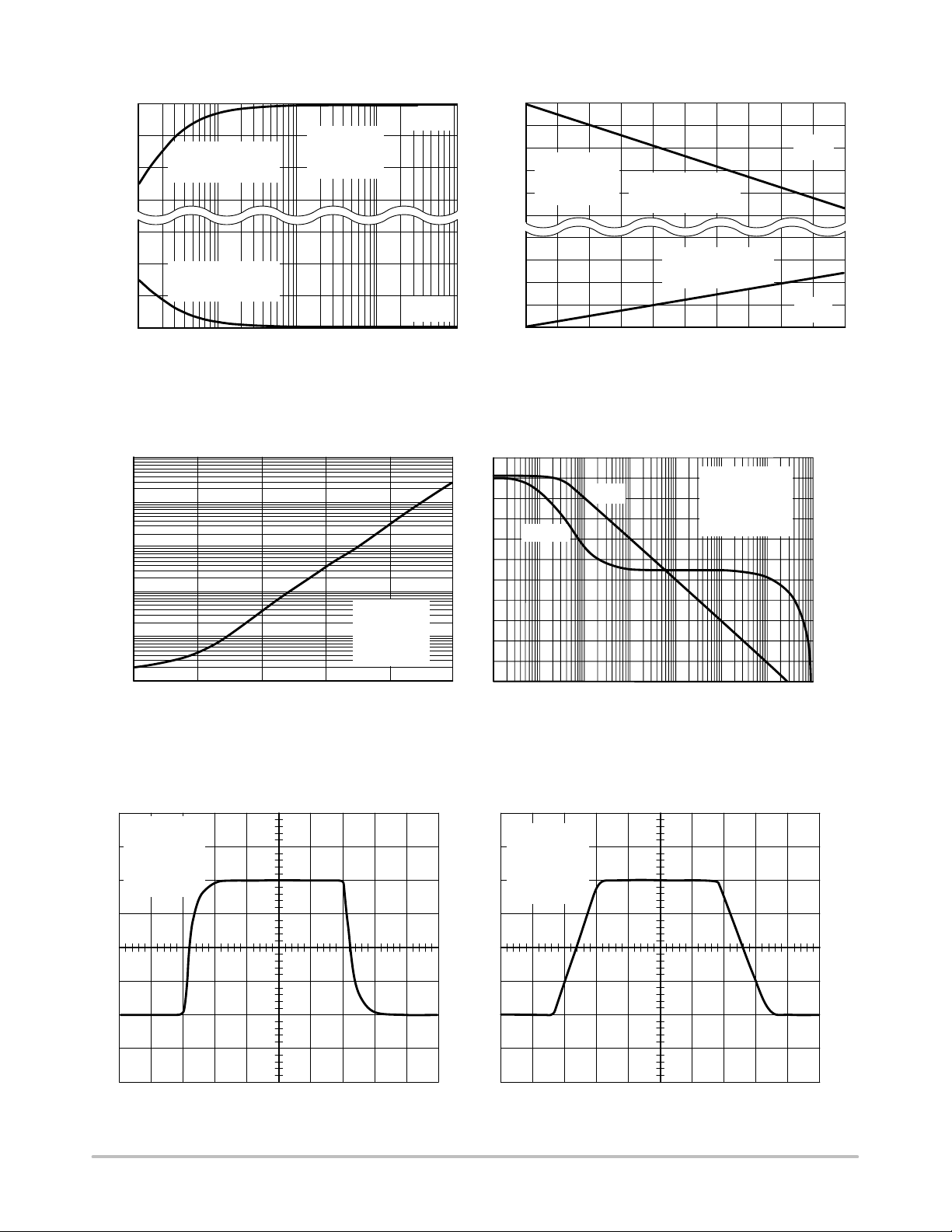
NCS2002, NCV2002
0
−200
−400
High State Output
Sourcing Current
VS = ±2.5 V
to Gnd
R
L
T
= 25°C
A
−600
600
400
, Output Saturation Voltage (mV)
200
sat
V
Low State Output
Sinking Current
0
100 1.0 k 10 k 100 k 1.0 M
, Load Resistance ()
R
L
Figure 2. Output Saturation Voltage versus
Load Resistance
10,000
1000
100
V
CC
−0.1
−0.2
−0.3
−0.4
VS = 2.5 V
to Gnd
R
L
= 25°C
T
A
High State Output
Sourcing Current
V
CC
−0.5
0.4
0
0.3
0.2
, Output Saturation Voltage (V)
sat
0.1
V
EE
V
0
0 4.0 16 20
Low State Output
Sinking Current
8.0 12
I
, Load Current (mA)
L
V
EE
Figure 3. Output Saturation Voltage versus
Load Current
100
0
20
60
80
Phase
Gain
VS = 2.5 V
R
= 100 k
L
= 25°C
T
A
Amp = 0.8 mV
10
VS = ±2.5 V
R
, Input Current (pA)
1.0
IB
I
C
A
= ∞
L
= 0
L
= 1.0
V
0
0 25 50 75 100 125
T
, Ambient Temperature (°C)
A
Figure 4. Input Bias Current versus
Temperature
VS = 2.5 V
R
= 10 k
L
= 10 pF
C
L
A
= 1.0
V
T
= 25°C
A
50 mV/Div
40
, Gain (dB)
V
A
20
0
1.0
10
10 k60100 k1.0 k100 1.0 M
f, Frequency (Hz)
Figure 5. Gain and Phase versus Frequency
VS = 2.5 V
R
= 10 k
L
= 10 pF
C
L
A
= 1.0
V
T
= 25°C
A
500 mV/Div
10 M
100
140
180
, Excess Phase (°)
Figure 6. Transient Response
t, Time (1.0 s/Div)t, Time (500 ns/Div)
Figure 7. Slew Rate
http://onsemi.com
5
Page 6
NCS2002, NCV2002
10
)PSRR, Power Supply Rejection Ratio (dB)
8.0
pp
VS = ±3.5 V
AV = 1.0
R
= 10 k
L
T
= 25°C
A
90
80
70
60
6.0
4.0
, Output Voltage (V
out
2.0
V
0
1.0 k
VS = ±2.5 V
VS = ±0.45 V
10 k 100 k 1.0 M
f, Frequency (Hz)
50
40
30
20
10
0
CMRR, Common Mode Rejection Ratio (dB)
10 100 1.0 k 10 k 100 k 1.0 M 10 M
f, Frequency (Hz)
Figure 8. Output Voltage versus Frequency Figure 9. Common Mode Rejection Ratio
versus Frequency
120
100
80
60
40
PSR −
PSR +
VS = ±2.5 V
R
= ∞
L
A
= 1.0
V
T
= 25°C
A
280
Output Pulsed Test
240
200
160
120
80
at 3% Duty Cycle
VS = ±2.5 V
R
= ∞
L
= 1.0
A
V
T
= 25°C
A
25°C
−40°C
85°C
20
0
10 100 1.0 k 10 k 100 k 1.0 M 10 M
f, Frequency (Hz)
Figure 10. Power Supply Rejection Ratio
versus Frequency
200
Output Pulsed Test
at 3% Duty Cycle
160
120
80
40
|, Output Short Circuit Current (mA)
SC
|I
0
0 ±1.0 ±2.0 ±2.5±0.5 ±1.5
VS, Supply Voltage (V)
25°C
±3.0 ±3.5
−40°C
85°C
40
|, Output Short Circuit Current (mA)
SC
|I
0
0 ±1.0 ±2.0 ±2.5±0.5 ±1.5
, Supply Voltage (V)
V
S
Figure 11. Output Short Circuit Sinking
Current versus Supply Voltage
1.0
0.8
25°C
0.6
0.4
|, Supply Current (mA)
D
|I
0.2
0
0 ±1.0 ±2.0 ±3.5±0.5 ±1.5
VS, Supply Voltage (V)
85°C
−40°C
±3.0 ±3.5
RL = ∞
A
= 1.0
V
±2.5 ±3.0
Figure 12. Output Short Circuit Sourcing
Current versus Supply Voltage
http://onsemi.com
Figure 13. Supply Current versus Supply
Voltage with No Load
6
Page 7

NCS2002, NCV2002
10
1.0
VS = ±0.5 V
V
= 0.4 V
0.1
out
RL = 2.0 k
T
= 25°C
A
pp
THD, Total Harmonic Distortion (%)
0.01
10
Figure 14. Total Harmonic Distortion versus
Frequency with 1.0 V Supply
10
AV = 1000
1.0
AV = 100
0.1
AV = 10
1.0 k100
f, Frequency (Hz)
AV = 1000
AV = 100
AV = 10
AV = 1.0
10 k 100 k
10
1.0
VS = ±0.5 V
V
= 0.4 V
0.1
out
RL = 10 k
= 25°C
T
A
pp
THD, Total Harmonic Distortion (%)
0.01
10 1.0 k 10 k100 100 k
f, Frequency (Hz)
Figure 15. Total Harmonic Distortion versus
Frequency with 1.0 V Supply
10
AV = 1000
1.0
AV = 100
0.1
AV = 10
AV = 1000
AV = 100
AV = 10
AV = 1.0
0.01
AV = 1.0
THD, Total Harmonic Distortion (%)
0.001
10 1.0 k100 100 k10 k
f, Frequency (Hz)
Figure 16. Total Harmonic Distortion versus
Frequency with 5.0 V Supply
1.5
1.4
+Slew Rate, VS = ±2.5 V
1.3
1.2
1.1
1.0
−Slew Rate, VS = ±0.5 V
−Slew Rate, VS = ±2.5 V
+Slew Rate, VS = ±0.5 V
0.9
0.8
SR, Slew Rate (V/µs)
0.7
0.6
RL = 10 k
C
= 10 pF
L
= 1.0
A
V
0.5
−50 −25 0 25 50 75 100
, Ambient Temperature (°C)
T
A
Figure 18. Slew Rate versus Temperature Figure 19. Gain Bandwidth Product versus
VS = ±2.5 V
V
= 4.0 V
out
RL = 2.0 k
T
= 25°C
A
pp
THD, Total Harmonic Distortion (%)
AV = 1.0
0.001
10 1.0 k100 100 k10 k
3.0
2.0
1.0
GBW, Gain Bandwidth Product (MHz)
0
0.01
125
−50 −25 0 25 50 75 100
VS = ±2.5 V
V
= 4.0 V
out
RL = 10 k
T
= 25°C
A
f, Frequency (Hz)
Figure 17. Total Harmonic Distortion versus
Frequency with 5.0 V Supply
VS = ±2.5 V
R
= 10 k
L
= 10 pF
C
L
T
, Ambient Temperature (°C)
A
Temperature
pp
125
http://onsemi.com
7
Page 8

NCS2002, NCV2002
60
40
VS = ±2.5 V
VS = ±0.5 V
20
, Gain (dB)
0
V
A
RL = 100 k
−20
T
VS = ±0.5 V
= 25°C
A
VS = ±2.5 V
Amp = 0.8 mV
−40
10 k 100 k 1.0 M 10 M 100 M
f, Frequency (Hz)
Figure 20. V oltage Gain and Phase versus
Frequency
100
Phase Margin
80
VS = ±2.5 V
60
40
, Gain Margin (dB)
m
A
20
= 10 k
R
L
C
= 10 pF
L
T
= 25°C
A
Gain Margin
60
100
100
Phase Margin
100
140
180
220
260
80
VS = ±2.5 V
60
R
C
40
, Gain Margin (dB)
m
A
m, Excess Phase (°)
20
0
−50 −25 0 25 50 75 100 125
Gain Margin
= 10 k
L
= 10 pF
L
80
60
40
20
0
TA, Ambient Temperature (°C)
Figure 21. Gain and Phase Margin versus
Temperature
100 100
80
60
40
20
100
Phase Margin
80
60
40
, Phase Margin (°)
, Gain Margin (dB)
m
m
A
Gain Margin
20
VS = ±2.5 V
R
= 10 k
L
= 100
A
V
T
= 25°C
A
80
60
40
20
m, Phase Margin (°)
, Phase Margin (°)
m
0
1.0 100 1.0 k 100 k
10
R
, Differential Source Resistance ()
t
10 k
Figure 22. Gain and Phase Margin versus
Differential Source Resistance
8.0
)
pp
6.0
4.0
, Output Voltage (V
V
out
2.0
RL = 10 k
A
= 100
V
T
= 25°C
A
0
0 ±0.5
±1.0 ±1.5 ±2.0 ±2.5 ±3.0 ±3.5
, Supply Voltage (V)
V
S
Figure 24. Output Voltage Swing versus
Supply Voltage
0
0
0
1.0 100 100010
CL, CapacitIve Load (pF)
Figure 23. Gain and Phase Margin versus
Output Load Capacitance
100
Phase Margin
80
60
40
, Gain Margin (dB)
m
A
Gain Margin
20
0
0 ±0.5 ±1.0 ±1.5 ±2.0 ±2.5 ±3.0 ±3.5
, Supply Voltage (V)
V
S
100
80
60
40
20
0
, Phase Margin (°)
m
Figure 25. Gain and Phase Margin versus
Supply Voltage
http://onsemi.com
8
Page 9

NCS2002, NCV2002
100
80
60
40
, Open Loop Voltage Gain (dB)
20
VOL
A
0
0 ±0.5
±1.0 ±1.5 ±2.0 ±2.5
, Supply Voltage (V)
V
S
Figure 26. Open Loop Voltage Gain versus
Supply Voltage
20
VS = ±0.9 V
15
R
= ∞
L
= 0
C
L
10
A
= 1.0
V
T
= 25°C
A
5
0
−5
−10
, Input Offset Voltage (mV)
IO
V
−15
−20
−1.0 −0.2−0.4−0.6
−0.8
V
, Common Mode Input Voltage (V)
CM
0 0.2 0.4 0.6 0.8 1.0
Figure 28. Input Offset Voltage versus Common
Mode Input Voltage Range, V
= 0.9 V
S
RL = 10 k
T
= 25°C
A
±3.0 ±3.5
20
VS = ±2.5 V
15
R
= ∞
L
= 0
C
10
L
A
= 1.0
V
T
= 25°C
5
A
0
−5
−10
, Input Offset Voltage (mV)
IO
V
−15
−20
−3.0 1.0 2.00−1.0 3.0−2.0
Figure 27. Input Offset Voltage versus Common
Mode Input Voltage Range, VS = 2.5 V
3.0
2.0
1.0
0
−1.0
Voltage Range (V)
, Input Common Mode
CM
V
−2.0
−3.0
0
Figure 29. Common−Mode Input Voltage Range
, Common Voltage Range (V)
V
CM
VIO = 5.0 mV
R
= ∞
L
= 0
C
L
A
= 1.0
V
T
= 25°C
A
±2.0 ±2.5±1.5±1.0 ±3.0±0.5
V
, Supply Voltage (V)
S
versus Power Supply Voltage
3.0
2.5
2.0
1.5
1.0
, Supply Current (A)
CC
I
0.5
0
0 ±0.5
4.0
3.5
3.0
2.5
2.0
1.5
, Enable Input Voltage (V)
RL = ∞
A
= 1.0
V
= 25°C
T
A
1.0
EN
V
0.5
0
±1.0 ±1.5 ±2.0 ±2.5 ±3.0 ±3.5 ±3.0
, Supply Voltage (V)
V
S
Figure 30. Supply Current versus
Supply Voltage (Disabled)
0
±0.5
V
, Supply Voltage (V)
S
±2.0 ±2.5±1.5±1.0
Figure 31. Enable Input Voltage versus
Supply Voltage
http://onsemi.com
9
V
EN(on)
V
EN(off)
AV = ∞
T
= 25°C
A
±3.5
Page 10

16
14
12
10
NCS2002, NCV2002
RL = 10 k
T
= 25°C
A
8.0
6.0
4.0
Propagation Delay (S)
2.0
0
0 ±0.5
±1.0 ±1.5 ±2.0 ±2.5
, SUPPLY VOLTAGE (V)
V
S
Figure 32. Propagation Delay versus Supply V oltage
APPLICATION INFORMATION AND OPERATING DESCRIPTION
GENERAL INFORMATION
The NCS2002 is an industry first rail−to−rail input,
rail−to−rail output amplifier that features guaranteed sub
one volt operation. This unique feature set is achieved with
the use of a modified analog CMOS process that allows the
implementation of depletion MOSFET devices. The
amplifier has a 1.0 MHz gain bandwidth product, 1.2 V/s
slew rate and is operational over a power supply range less
than 0.9 V to as high as 7.0 V.
Inputs
The input topology chosen for this device series is
unconventional when compared to most low voltage
operational amplifiers. It consists of an N−channel depletion
mode differential transistor pair that drives a folded cascade
stage and current mirror. This configuration extends the
input common mode voltage range to encompass the V
EE
and VCC power supply rails, even when powered from a
combined total of less than 0.9 volts. Figures 27, 28 and 29
show the input common mode voltage range versus power
supply voltage.
The differential input stage is laser trimmed in order to
minimize offset voltage. The N−channel depletion mode
MOSFET input stage exhibits an extremely low input bias
current of less than 10 pA. The input bias current versus
temperature is shown in Figure 4. Either one or both inputs
can be biased as low as V
minus 300 mV to as high as
EE
7.0 V without causing damage to the device. If the input
common mode voltage range is exceeded, the output will not
display a phase reversal. If the maximum input positive or
negative voltage ratings are to be exceeded, a series resistor
must be used to limit the input current to less than 2.0 mA.
t
on
t
off
±3.0 ±3.5
The ultra low input bias current of the NCS2002 allows
the use of extremely high value source and feedback resistor
without reducing the amplifier’s gain accuracy. These high
value resistors, in conjunction with the device input and
printed circuit board parasitic capacitances C
, will add an
in
additional pole to the single pole amplifier in Figure 33. If
low enough in frequency, this additional pole can reduce the
phase margin and significantly increase the output settling
time. The effects of C
, can be canceled by placing a zero
in
into the feedback loop. This is accomplished with the
addition of capacitor Cfb. An approximate value for Cfb can
be calculated by:
Rin C
C
fb
C
R
Input
Cin = Input and printed circuit board capacitance
in
C
in
Figure 33. Input Capacitance Pole Cancellation
in
R
fb
fb
R
fb
−
+
Output
http://onsemi.com
10
Page 11

NCS2002, NCV2002
Output
The output stage consists of complimentary P and N
channel devices connected to provide rail−to−rail output
drive. With a 2.0 k load, the output can swing within 50 mV
of either rail. It is also capable of supplying over 75 mA
when powered from 5.0 V and 1.0 mA when powered from
0.9 V.
When connected as a unity gain follower, the NCS2002
can directly drive capacitive loads in excess of 820 pF at
room temperature without oscillating but with significantly
reduced phase margin. The unity gain follower
configuration exhibits the highest bandwidth and is most
prone to oscillations when driving a high value capacitive
load. The capacitive load in combination with the
amplifier’s output impedance, creates a phase lag that can
result in an under−damped pulse response or a continuous
oscillation. Figure 35 shows the effect of driving a large
capacitive load in a voltage follower type of setup. When
driving capacitive loads exceeding 820 pF, it is
recommended to place a low value isolation resistor
between the output of the op amp and the load, as shown in
Figure 34. The series resistor isolates the capacitive load
from the output and enhances the phase margin. Refer to
Figure 36. Larger values of R will result in a cleaner output
waveform but excessively large values will degrade the
large signal rise and fall time and reduce the output
amplitude. Depending upon the capacitor characteristics,
the isolation resistor value will typically be between 50 to
500 . The output drive capability for resistive and
capacitive loads is shown in Figures 2, 3, and 23.
Input
Figure 34. Capacitance Load Isolation
+
−
Isolation resistor R = 50 to 500
R
Output
C
L
Note that the lowest phase margin is observed at cold
temperature and low supply voltage.
Enable Pin
The enable pin allows the user to externally control the
device. if the enable pin is pulled below the input disable
threshold voltage (V
< 45% VCC), the amplifier is
EN
disabled. Once the enable pin is taken above the threshold
voltage (VEN = 60% VCC), the amplifier will turn on. In the
event the enable pin is not connected, the amplifier will
remain on by default
http://onsemi.com
11
Page 12

NCS2002, NCV2002
V
in
VS = ±0.45 V
V
= 0.8 Vpp
in
R = 0
C
= 820 pF
L
A
= 1.0
V
= 25°C
T
A
V
out
Figure 35. Small Signal Transient Response with Large Capacitive Load
V
in
V
out
VS = ±0.45 V
V
= 0.8 Vpp
in
R = 51
= 820 pF
C
L
A
= 1.0
V
T
= 25°C
A
Figure 36. Small Signal Transient Response with Large
Capacitive Load and Isolation Resistor.
http://onsemi.com
12
Page 13

0.9 V
C
T
1.0 nF
R
1a
470 k
470 k
NCS2002, NCV2002
R
T
470 k
Output Voltage
0.9 V
Timing Capacitor
−
= 1.5 kHz
f
+
O
Voltage
The non−inverting input threshold levels are set so that
the capacitor voltage oscillates between 1/3 and 2/3 of
. This requires the resistors R1a, R1b and R2 to be of
V
CC
equal value. The following formula can be used to
R
R
1b
2
470 k
approximate the output frequency.
Figure 37. 0.9 V Square Wave Oscillator
0.67 V
0.33 V
f
O
V
CC
0
CC
CC
1.39 R
1
TCT
D
1
cww
10 k
1N4148
Output Voltage
1.0 M
D
10 k
2
1N4148
Timing Capacitor
Voltage
cw
V
C
T
1.0 nF
CC
−
f
O
+
Output Voltage
Timing Capacitor
Voltage
R
1a
470 k
V
CC
R
1b
470 k
R
2
470 k
The timing capacitor C
through diode D
, allowing a variable duty cycle. The pulse width of the
1
signal can be programmed by adjusting the value of the trimpot. The capacitor voltage will oscillate between 1/3 and 2/3 of V
V
CC
0
0.67 V
CC
0.33 V
CC
Clock−wise, Low Duty Cycle
V
CC
0
0.67 V
CC
0.33 V
CC
Counter−Clock−wise, High Duty Cycle
will charge through diode D2 and discharge
T
, since all the
CC
resistors at the non−inverting input are of equal value.
Figure 38. Variable Duty Cycle Pulse Generator
http://onsemi.com
13
Page 14

C
in
10 F
NCS2002, NCV2002
R
1
1.0 M
2.5 V
R
3
+
−
−2.5 V
R
2
1.0 M
Figure 39. Positive Capacitance Multiplier
1.0 k
≈
C
eff.
10,000 µF
R
R
1
C
in
3
A
C
f
400 pF
R
f
100 k
R
10 k
1
0.5 V
+
−
−0.5 V
V
O
R
2
10 k
V
in
C
1
80 nF
f
f
f
L
2 R1C
f
H
2 RfC
Af 1
L
1
1
R
f
R
2
f
H
200 Hz
1
4.0 kHz
f
11
Figure 40. 1.0 V Voiceband Filter
http://onsemi.com
14
Page 15

NCS2002, NCV2002
V
supply
V
CC
V
in
Figure 41. High Compliance Current Sink
+
−
R
I
sink
sense
R
sense
V
in
I
R
s
sense
1.0 V
R
3
V
L
1.0 k
R
R
L
1
1.0 k
R
4
1.0 k
+
−
R
5
2.4 k
V
O
I
s
V
O
435 mA 34.7 mV
212 mA 36.9 mV
75
R
6
R
2
For best performance, use low
tolerance resistors.
3.3 k
Figure 42. High Side Current Sense
http://onsemi.com
15
Page 16

0.05 (0.002)
NCS2002, NCV2002
PACKAGE DIMENSIONS
TSOP−6
CASE 318G−02
ISSUE I
NOTES:
A
L
456
S
1
23
B
D
G
M
C
H
K
J
1. DIMENSIONING AND TOLERANCING PER ANSI
Y14.5M, 1982.
2. CONTROLLING DIMENSION: MILLIMETER.
3. MAXIMUM LEAD THICKNESS INCLUDES LEAD
FINISH THICKNESS. MINIMUM LEAD THICKNESS
IS THE MINIMUM THICKNESS OF BASE
MATERIAL.
4. DIMENSIONS A AND B DO NOT INCLUDE MOLD
FLASH, PROTRUSIONS, OR GATE BURRS.
DIM MIN MAX MIN MAX
A 0.1142 0.12202.90 3.10
B 0.0512 0.06691.30 1.70
C 0.0354 0.04330.90 1.10
D 0.0098 0.01970.25 0.50
G 0.0335 0.04130.85 1.05
H 0.0005 0.00400.013 0.100
J 0.0040 0.01020.10 0.26
K 0.0079 0.02360.20 0.60
L 0.0493 0.06101.25 1.55
M 0 10 0 10
S 0.0985 0.11812.50 3.00
INCHESMILLIMETERS
ON Semiconductor and are registered trademarks of Semiconductor Components Industries, LLC (SCILLC). SCILLC reserves the right to make changes without further notice
to any products herein. SCILLC makes no warranty, representation or guarantee regarding the suitability of its products for any particular purpose, nor does SCILLC assume any liability
arising out of the application or use of any product or circuit, and specifically disclaims any and all liability, including without limitation special, consequential or incidental damages.
“Typical” parameters which may be provided in SCILLC data sheets and/or specifications can and do vary in different applications and actual performance may vary over time. All
operating parameters, including “Typicals” must be validated for each customer application by customer’s technical experts. SCILLC does not convey any license under its patent rights
nor the rights of others. SCILLC products are not designed, intended, or authorized for use as components in systems intended for surgical implant into the body, or other applications
intended to support or sustain life, or for any other application in which the failure of the SCILLC product could create a situation where personal injury or death may occur. Should
Buyer purchase or use SCILLC products for any such unintended or unauthorized application, Buyer shall indemnify and hold SCILLC and its officers, employees, subsidiaries, affiliates,
and distributors harmless against all claims, costs, damages, and expenses, and reasonable attorney fees arising out of, directly or indirectly, any claim of personal injury or death
associated with such unintended or unauthorized use, even if such claim alleges that SCILLC was negligent regarding the design or manufacture of the part. SCILLC is an Equal
Opportunity/Affirmative Action Employer. This literature is subject to all applicable copyright laws and is not for resale in any manner.
PUBLICATION ORDERING INFORMATION
LITERATURE FULFILLMENT:
Literature Distribution Center for ON Semiconductor
P.O. Box 5163, Denver, Colorado 80217 USA
Phone: 303−675−2175 or 800−344−3860 Toll Free USA/Canada
Fax: 303−675−2176 or 800−344−3867 Toll Free USA/Canada
Email: orderlit@onsemi.com
N. American Technical Support: 800−282−9855 Toll Free
USA/Canada
Japan: ON Semiconductor, Japan Customer Focus Center
2−9−1 Kamimeguro, Meguro−ku, Tokyo, Japan 153−0051
Phone: 81−3−5773−3850
http://onsemi.com
ON Semiconductor Website: http://onsemi.com
Order Literature: http://www.onsemi.com/litorder
For additional information, please contact your
local Sales Representative.
NCS2002/D
16
Page 17

Copyright © Each Manufacturing Company.
All Datasheets cannot be modified without permission.
This datasheet has been download from :
www.AllDataSheet.com
100% Free DataSheet Search Site.
Free Download.
No Register.
Fast Search System.
www.AllDataSheet.com
 Loading...