

NCP9004
2.65 W Filterless Class−D
Audio Power Amplifier
The NCP9004 is a cost−effective mono Class−D audio power
amplifier capable of delivering 2.65 W of continuous average power
to 4.0 from a 5.0 V supply in a Bridge Tied Load (BTL)
configuration. Under the same conditions, the output power stage can
provide 1.4 W to a 8.0 BTL load with less than 1% THD+N. For
cellular handsets or PDAs it offers space and cost savings because no
output filter is required when using inductive tranducers. With more
than 90% efficiency and very low shutdown current, it increases the
lifetime of your battery and drastically lowers the junction
temperature.
The NCP9004 processes analog inputs with a pulse width
modulation technique that lowers output noise and THD when
compared to a conventional sigma−delta modulator. The device allows
independent gain while summing signals from various audio sources.
Thus, in cellular handsets, the earpiece, the loudspeaker and even the
melody ringer can be driven with a single NCP9004. Due to its low
42 V noise floor, A−weighted, a clean listening is guaranteed no
matter the load sensitivity.
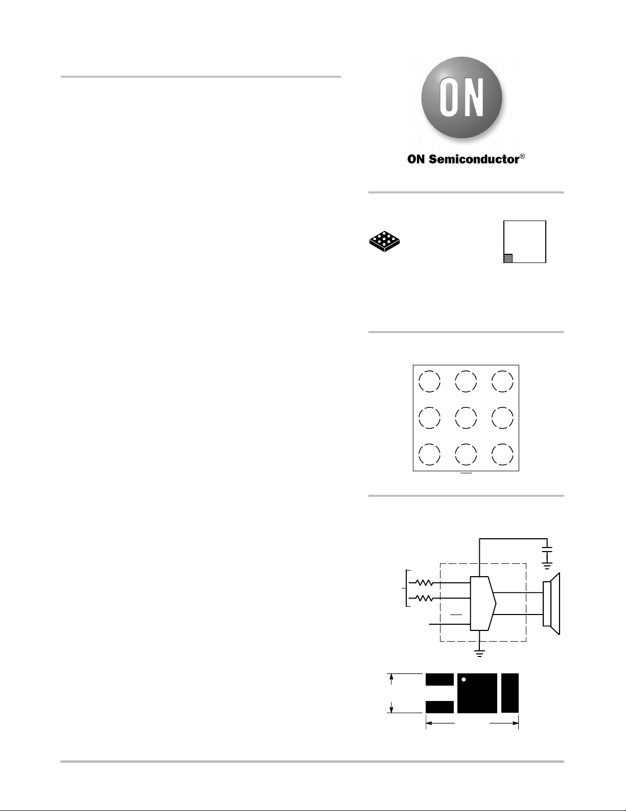
http://onsemi.com
9−PIN FLIP−CHIP CSP
FC SUFFIX
1
CASE 499E
MAQ = Device Code
A = Assembly Location
Y = Year
WW = Work Week
G = Pb−Free Package
PIN CONNECTIONS
9−Pin Flip−Chip CSP
MARKING
DIAGRAM
MAQG
AYWW
1
Features
• Optimized PWM Output Stage: Filterless Capability
• Efficiency up to 90%
Low 2.5 mA Typical Quiescent Current
• Large Output Power Capability: 1.4 W with 8.0 Load and
THD+N < 1%
• Wide Supply Voltage Range: 2.5−5.5 V Operating Voltage
• High Performance, THD+N of 0.03% @ V
RL = 8.0 , P
= 100 mW
out
= 5.0 V,
p
• Excellent PSRR (−65 dB): No Need for Voltage Regulation
• Surface Mounted Package 9−Pin Flip−Chip CSP (SnPb and Pb−Free)
• Fully Differential Design. Eliminates Two Input Coupling Capacitors
• Very Fast Turn On/Off Times with Advanced Rising and Falling
Gain Technique
• External Gain Configuration Capability
• Internally Generated 250 kHz Switching Frequency
• Short Circuit Protection Circuitry
• “Pop and Click” Noise Protection Circuitry
Applications
• Cellular Phone
• Portable Electronic Devices
• PDAs and Smart Phones
• Portable Computer
A1
B1
VP
C1
INM
See detailed ordering and shipping information on page 16 of
this data sheet.
Microcontroller
ORDERING INFORMATION
Audio
Input
from
DAC
1.6 mm
R
R
Input from
R
i
R
i
i
i
A2
GNDINP OUTM
B2
VP
C2
SD OUTP
(Top View)
VP
INP
INM
SD
GND
3.7 mm
A3
B3
GND
C3
Cs
OUTM
OUTP
Cs
© Semiconductor Components Industries, LLC, 2006
August, 2006 − Rev. 2
Solution Size
1 Publication Order Number:
NCP9004/D
NCP9004
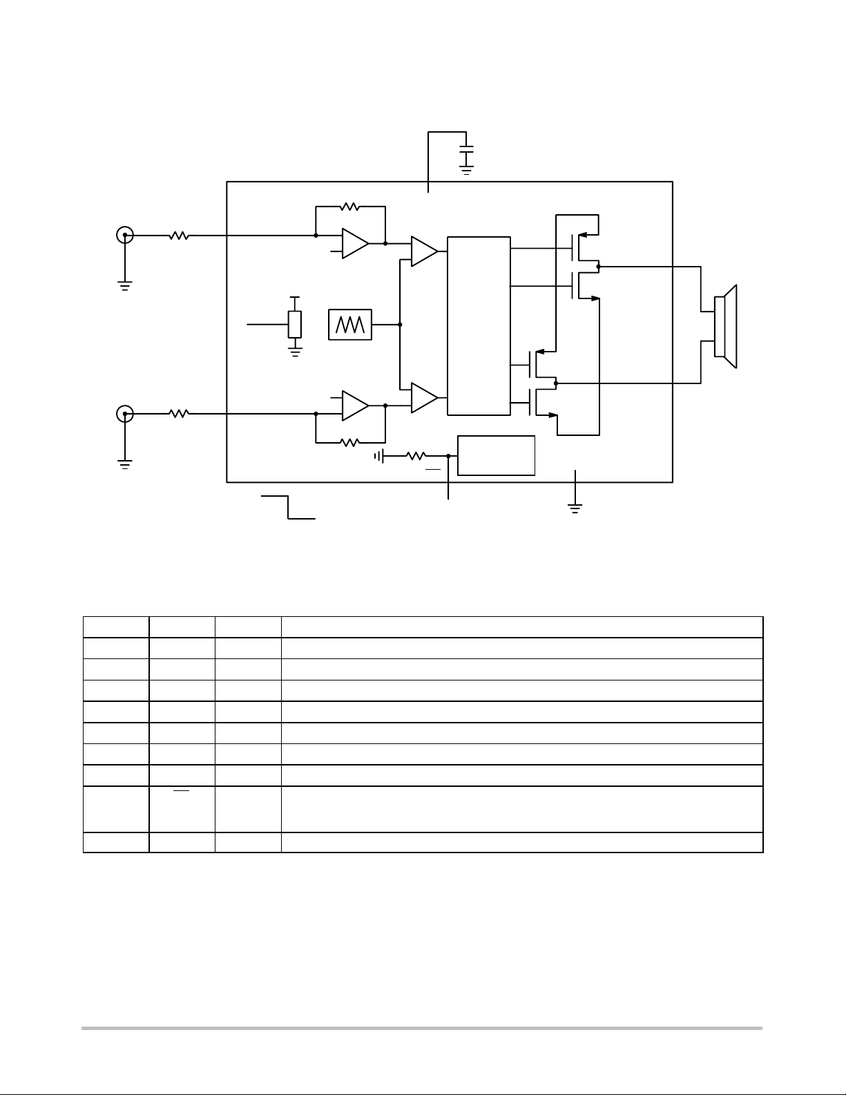
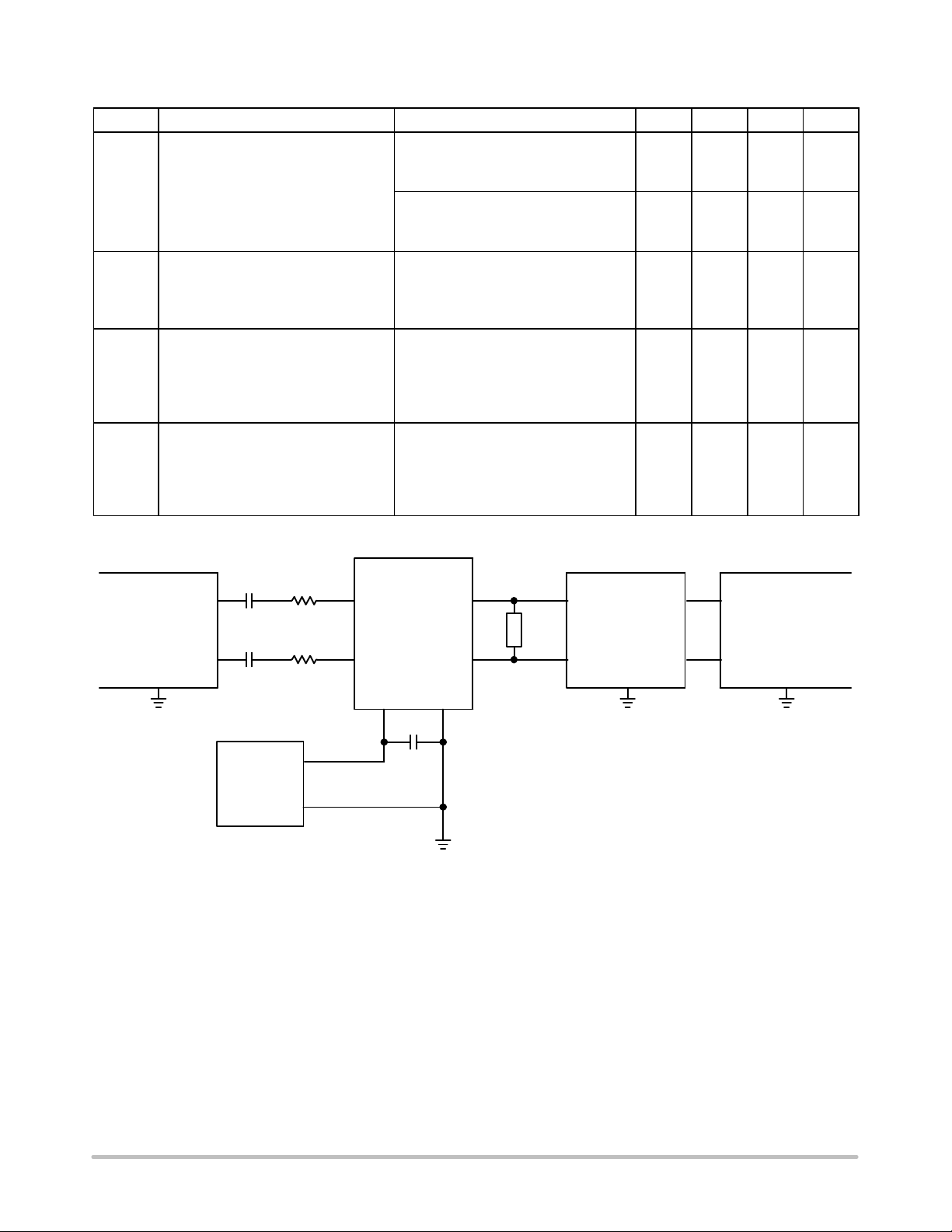
TYPICAL APPLICATION
BATTERY
Cs
R
f
R
i
INP
V
p
BYPASS
Negative
Differential
Input
V
BYPASS
p
GENERATOR
RAMP
Data
Processor
INTERNAL
BIASING
R
i
INM
BYPASS
R
f
300 k
Shutdown
Control
Positive
Differential
Input
V
ih
V
il
SD
Figure 1. Typical Application
PIN DESCRIPTION
Pin No. Symbol Type Description
A1 INP I Positive Differential Input.
A2 GND I Analog Ground.
A3 OUTM O Negative BTL Output.
B1 V
B2 V
p
p
B3 GND I Analog Ground.
C1 INM I Negative Differential Input.
C2 SD I
C3 OUTP O Positive BTL Output.
I Power Analog Positive Supply. Range: 2.5 V – 5.5 V.
I Power Analog Positive Supply. Range: 2.5 V – 5.5 V.
The device enters in Shutdown Mode when a low level is applied on this pin. An internal 300 k
resistor will force the device in shutdown mode if no signal is applied to this pin. It also helps to
save space and cost.
GND
OUTM
OUTP
8
=
L
R
http://onsemi.com
2
NCP9004
MAXIMUM RATINGS
Symbol Rating Max Unit
V
p
V
in
I
out
P
d
T
A
T
J
T
stg
R
JA
−
−
− Latchup Current @ TA = 85°C (Note 6) $70 mA
MSL Moisture Sensitivity (Note 7) Level 1
Stresses exceeding Maximum Ratings may damage the device. Maximum Ratings are stress ratings only. Functional operation above the
Recommended Operating Conditions is not implied. Extended exposure to stresses above the Recommended Operating Conditions may affect
device reliability.
1. The device is protected by a current breaker structure. See “Current Breaker Circuit” in the Description Information section for more
information.
2. The thermal shutdown is set to 160°C (typical) avoiding irreversible damage to the device due to power dissipation.
3. For the 9−Pin Flip−Chip CSP package, the R
50 mm2 total area and also 135°C/W with 500 mm2. When using ground and power planes, the value is around 90°C/W, as specified in table.
4. Human Body Model: 100 pF discharged through a 1.5 k resistor following specification JESD22/A114. B2 pin (Vp) qualified at 1500 V.
5. Machine Model: 200 pF discharged through all pins following specification JESD22/A115.
6. Latchup Testing per JEDEC Standard JESD78.
7. Moisture Sensitivity Level (MSL): 1 per IPC/JEDEC standard: J−STD−020A.
Supply Voltage Active Mode
Shutdown Mode
6.0
7.0
V
Input Voltage −0.3 to VCC +0.3 V
Max Output Current (Note 1) 1.5 A
Power Dissipation (Note 2) Internally Limited −
Operating Ambient Temperature −40 to +85 °C
Max Junction Temperature 150 °C
Storage Temperature Range −65 to +150 °C
Thermal Resistance Junction−to−Air 90 (Note 3) °C/W
ESD Protection
Human Body Model (HBM) (Note 4)
Machine Model (MM) (Note 5)
is highly dependent of the PCB Heatsink area. For example, R
JA
> 2000
> 200
can equal 195°C/W with
JA
V
http://onsemi.com
3
NCP9004
ELECTRICAL CHARACTERISTICS (Limits apply for T
= +25°C unless otherwise noted)
A
Symbol Characteristic Conditions Min Typ Max Unit
V
I
Operating Supply Voltage TA = −40°C to +85°C 2.5 − 5.5 V
p
Supply Quiescent Current
dd
Vp = 3.6 V, RL = 8.0
= 5.5 V, No Load
V
p
−
−
2.15
2.61
−
mA
−
Vp from 2.5 V to 5.5 V, No Load
TA = −40°C to +85°C
I
sd
Shutdown Current
Vp = 4.2 V
TA = +25°C
TA = +85°C
−
−
−
−
0.42
0.45
4.6
0.8
−
Vp = 5.5 V
TA = +25°C
TA = +85°C
V
V
F
Shutdown Voltage High
sdih
Shutdown Voltage Low
sdil
Switching Frequency Vp from 2.5 V to 5.5 V
sw
−
−
0.8
0.9
1.5
−
1.2 − − V
− − 0.4 V
190 250 310 kHz
TA = −40°C to +85°C
G Gain
RL = 8.0 285 k
R
i
300 k
R
i
315 k
R
i
Rs Resistance from SD to GND − − 300 −
Vos Output Offset Voltage Vp = 5.5 V − 6.0 − mV
To n Turn On Time Vp from 2.5 V to 5.5 V − 9.0 − ms
To ff Turn Off Time Vp from 2.5 V to 5.5 V − 5.0 − ms
Ts d Thermal Shutdown Temperature − − 160 − °C
Vn Ouput Noise Voltage
Po RMS Output Power
V
= 3.6 V, f = 20 Hz to 20 kHz
p
no weighting filter
with A weighting filter
no weighting filter
with A weighting filter
RL = 8.0 , f = 1.0 kHz, THD+N < 1%
V
= 2.5 V
p
V
= 3.0 V
p
V
= 3.6 V
p
V
= 4.2 V
p
V
= 5.0 V
p
Vrms
−
−
−
−
−
−
−
−
−
65
42
70
48
0.32
0.48
0.7
0.97
1.38
−
−
−
Vrms
−
−
−
−
−
−
RL = 8.0 , f = 1.0 kHz, THD+N < 10%
V
p
V
p
V
p
V
p
V
p
= 2.5 V
= 3.0 V
= 3.6 V
= 4.2 V
= 5.0 V
−
−
−
−
−
0.4
0.59
0.87
1.19
1.7
−
−
−
−
−
RL = 4.0 , f = 1.0 kHz, THD+N < 1%
V
p
V
p
V
p
V
p
V
p
= 2.5 V
= 3.0 V
= 3.6 V
= 4.2 V
= 5.0 V
−
−
−
−
−
0.49
0.72
1.06
1.62
2.12
−
−
−
−
−
RL = 4.0 , f = 1.0 kHz, THD+N < 10%
V
p
V
p
V
p
V
p
V
p
= 2.5 V
= 3.0 V
= 3.6 V
= 4.2 V
= 5.0 V
−
−
−
−
−
0.6
0.9
1.33
2.0
2.63
−
−
−
−
−
A
A
V
V
k
W
W
W
W
http://onsemi.com
4
NCP9004
ELECTRICAL CHARACTERISTICS (Limits apply for T
= +25°C unless otherwise noted)
A
Symbol UnitMaxTypMinConditionsCharacteristic
− Efficiency
RL = 8.0 , f = 1.0 kHz
= 5.0 V, P
V
p
V
= 3.6 V, P
p
out
out
= 1.2 W
= 0.6 W
RL = 4.0 , f = 1.0 kHz
THD+N Total Harmonic Distortion + Noise
V
= 5.0 V, P
p
= 3.6 V, P
V
p
V
= 5.0 V, RL = 8.0 ,
p
f = 1.0 kHz, P
V
= 3.6 V, RL = 8.0 ,
p
f = 1.0 kHz, P
= 2.0 W
out
= 1.0 W
out
= 0.25 W
out
= 0.25 W
out
CMRR Common Mode Rejection Ratio Vp from 2.5 V to 5.5 V
Vic = 0.5 V to V
V
= 3.6 V, Vic = 1.0 V
p
− 0.8 V
p
f = 217 Hz
f = 1.0 kHz
PSRR Power Supply Rejection Ratio
V
p_ripple_pk−pk
= 200 mV, RL = 8.0 ,
Inputs AC Grounded
V
= 3.6 V
p
f = 217 kHz
f = 1.0 kHz
%
−
−
91
90
−
−
%
−
−
82
81
−
−
%
−
−
0.05
0.09
−
−
dB
−
pp
−
−
−62
−56
−57
−
−
−
dB
−
−
−62
−65
−
−
NCP9004
INP
INM
VP
OUTM
OUTP
GND
Load
30 kHz
Low Pass
Filter
+
Measurement
Input
−
Audio Input
Signal
C
R
i
i
+
C
i
R
−
i
4.7 F
+
Power
Supply
−
Figure 2. Test Setup for Graphs
NOTES:
1. Unless otherwise noted, Ci = 100 nF and Ri= 150 k. Thus, the gain setting is 2 V/V and the cutoff frequency of the
input high pass filter is set to 10 Hz. Input capacitors are shorted for CMRR measurements.
2. To closely reproduce a real application case, all measurements are performed using the following loads:
RL = 8 means Load = 15 H + 8 + 15 H
RL = 4 means Load = 15 H + 4 + 15 H
Very low DCR 15 H inductors (50 m) have been used for the following graphs. Thus, the electrical load
measurements are performed on the resistor (8 or 4 ) in differential mode.
3. For Efficiency measurements, the optional 30 kHz filter is used. An RC low−pass filter is selected with
(100 , 47 nF) on each PWM output.
http://onsemi.com
5
NCP9004
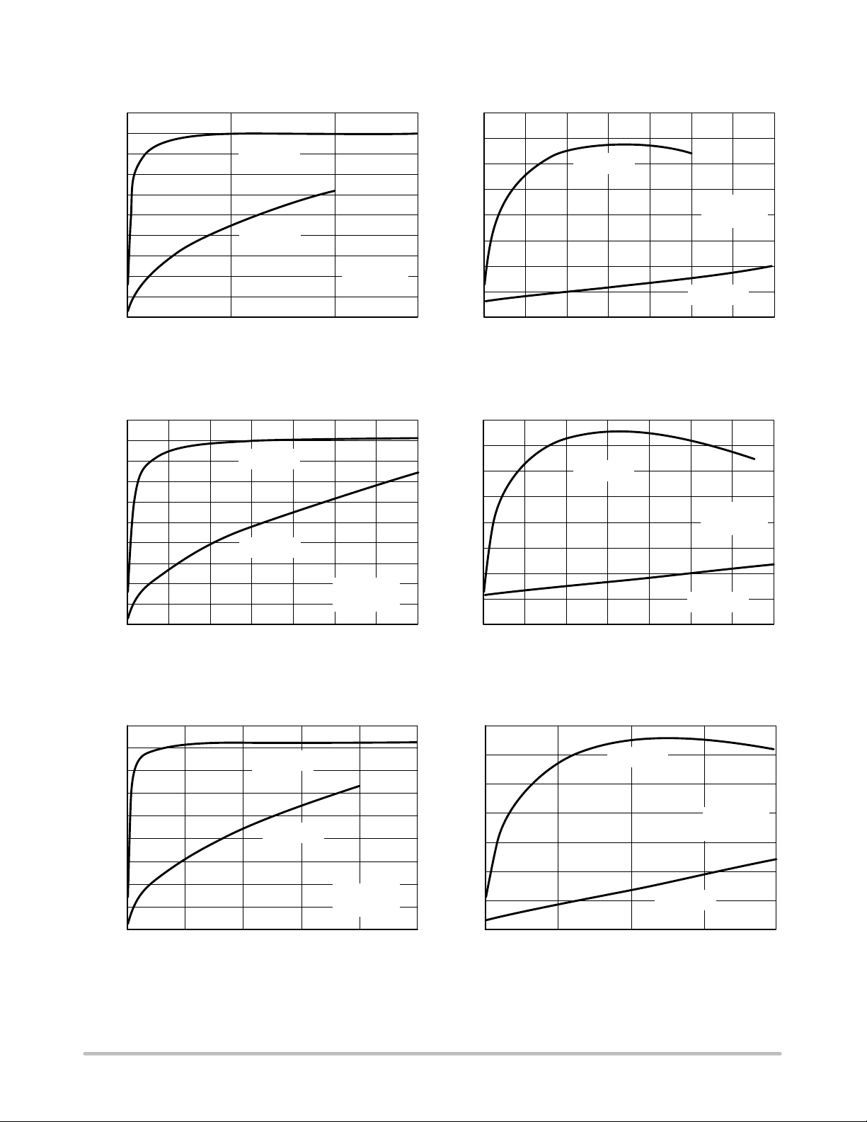
TYPICAL CHARACTERISTICS
100
90
80
70
60
50
40
30
EFFICIENCY (%)
20
10
0
0 0.5 1.0
Figure 3. Efficiency vs. P
NCP9004
Class AB
P
(W)
out
Vp = 5 V
R
out
Vp = 5 V, RL = 8 , f = 1 kHz
100
90
80
70
60
50
40
30
EFFICIENCY (%)
20
10
0
0 0.1 0.2 0.3 0.4 0.5 0.6 0.7
Figure 5. Efficiency vs. P
NCP9004
Class AB
P
(W)
out
Vp = 3.6 V
RL = 8
out
Vp = 3.6 V, RL = 8 , f = 1 kHz
= 8
L
100
90
80
70
60
50
40
DIE TEMPERATURE (°C)
30
20
0 0.2 0.4
60
55
50
45
40
35
30
DIE TEMPERATURE (°C)
25
20
0 0.1 0.2
Class AB
NCP9004
0.6 0.8 1.0 1.2 1.4
P
(W)
out
Figure 4. Die Temperature vs. P
Vp = 5 V, RL = 8 , f = 1 kHz @ T
Class AB
NCP9004
0.3 0.4
P
(W)
out
0.5 0.6 0.7
Figure 6. Die Temperature vs. P
Vp = 3.6 V, RL = 8 , f = 1 kHz @ T
Vp = 5 V
R
= 8
L
out
= +25°C
A
Vp = 3.6 V
RL = 8
out
= +25°C
A
90
80
70
60
50
40
30
EFFICIENCY %
20
10
0
0 0.5 1.0 1.5
Figure 8. Efficiency vs. P
Vp = 5 V, RL = 4 , f = 1 kHz
NCP9004
Class AB
P
(W)
out
Vp = 5 V
RL = 4
2.0 2.5
out
160
140
120
100
80
60
DIE TEMPERATURE (°C)
40
20
http://onsemi.com
6
Class AB
0 0.5 1.0
P
(W)
out
Figure 7. Die Temperature vs. P
Vp = 5 V, RL = 4 , f = 1 kHz @ T
NCP9004
1.5 2.0
Vp = 5 V
RL = 4
out
= +25°C
A
NCP9004
TYPICAL CHARACTERISTICS
90
80
70
60
50
40
30
EFFICIENCY %
20
10
0
0 0.4 0.8 1.2
0.2 0.6 1.0
Figure 9. Efficiency vs. P
NCP9004
Class AB
P
(W)
out
Vp = 3.6 V
RL = 4
out
Vp = 3.6 V, RL = 4 , f = 1 kHz
10
Vp = 5.0 V
RL = 8
1.0
f = 1 kHz
100
90
80
70
60
50
40
DIE TEMPERATURE (°C)
30
20
0 0.2 0.4
Figure 10. Die Temperature vs. P
Vp = 3.6 V, RL = 4 , f = 1 kHz @ T
10
Vp = 4.2 V
RL = 8
1.0
f = 1 kHz
Class AB
0.6 0.8
P
(W)
out
Vp = 3.6 V
RL = 4
NCP9004
A
1.0
out
= +25°C
THD+N (%)
0.1
0.01
0 0.2 0.4 0.6 0.8 1.0 1.2 1.4 1.6
P
(W)
out
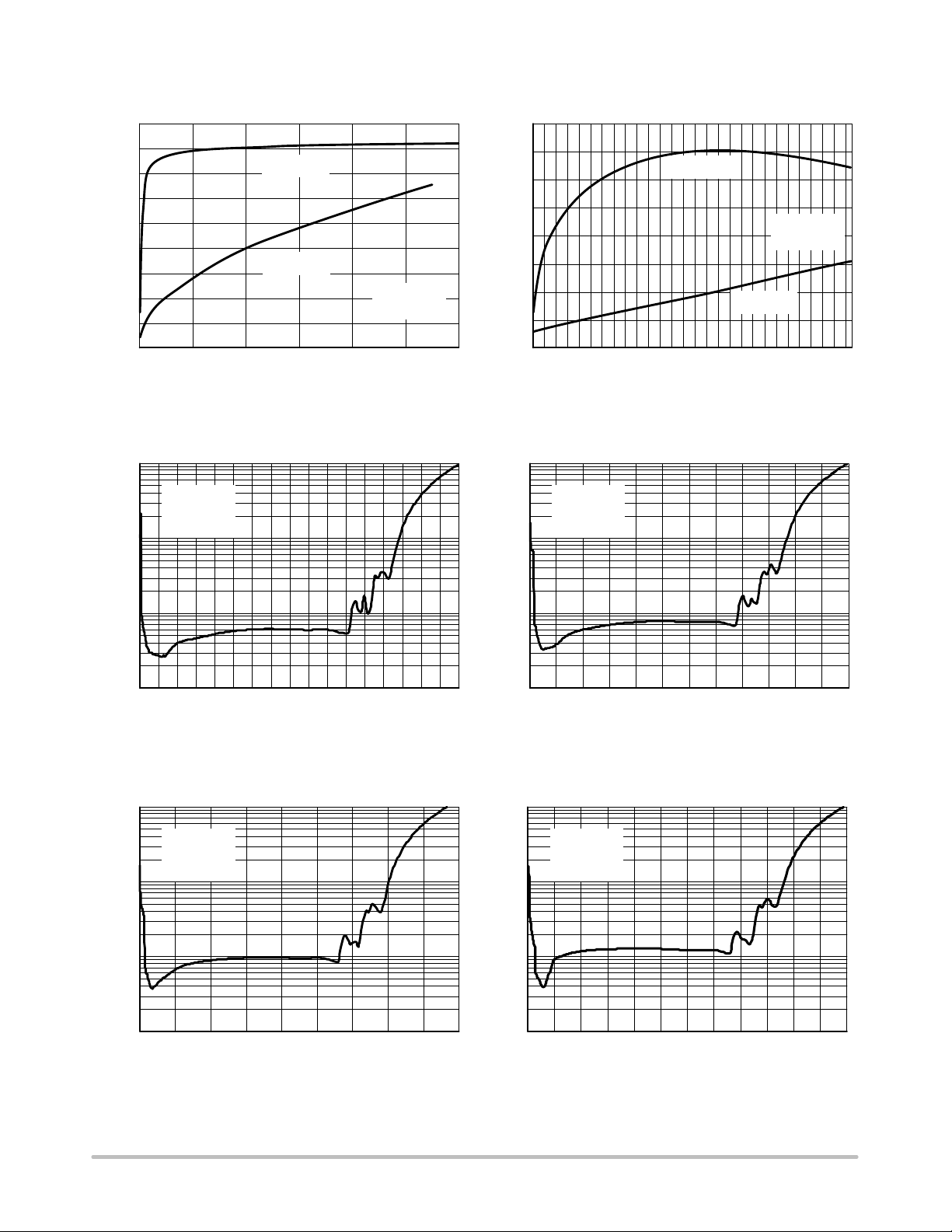
Figure 11. THD+N vs. P
Vp = 5 V, RL = 8 , f = 1 kHz
10
Vp = 3.6 V
RL = 8
1.0
THD+N (%)
0.1
0.01
f = 1 kHz
0 0.2 0.4 0.6 0.8
P
(W)
out
out
THD+N (%)
0.1
0.01
0 0.2 0.4 0.6 0.8 1.0 1.2
P
(W)
out
Figure 12. THD+N vs. P
out
Vp = 4.2 V, RL = 8 , f = 1 kHz
10
Vp = 3 V
RL = 8
1.0
THD+N (%)
0.1
0.01
f = 1 kHz
0 0.1 0.2 0.3 0.4 0.5 0.6
P
(W)
out
Figure 13. THD+N vs. P
out
Vp = 3.6 V, RL = 8 , f = 1 kHz
http://onsemi.com
7
Figure 14. THD+N vs. P
out
Vp = 3 V, RL = 8 , f = 1 kHz

NCP9004
TYPICAL CHARACTERISTICS
10
Vp = 2.5 V
R
= 8
L
1.0
THD+N (%)
0.1
0.01
f = 1 kHz
0 0.1 0.2 0.3 0.4
P
(W)
out
Figure 15. THD+N vs. Pout
= 2.5 V, RL = 8 , f = 1 kHz
V
p
10
Vp = 4.2 V
RL = 4
1.0
f = 1 kHz
10
Vp = 5 V
RL = 4
f = 1 kHz
1.0
THD+N (%)
0.1
0.01
0 0.5 1.0
10
Vp = 3.6 V
RL = 4
1.0
f = 1 kHz
1.5 2.0
P
(W)
out
Figure 16. THD+N vs. Pout
= 5 V, RL = 4 , f = 1 kHz
V
p
2.5
THD+N (%)
0.1
0.01
0 0.5 1.0 1.5 2.0
P
(W)
out
Figure 17. THD+N vs. Pout
= 4.2 V, RL = 4 , f = 1 kHz
V
p
10
Vp = 3 V
RL = 4
f = 1 kHz
1.0
THD+N (%)
0.1
0
0.2 0.4 0.6 0.8
P
(W)
out
1.0
THD+N (%)
0.1
0.01
0 0.4 0.8 1.2 1.4
0.2 0.6 1.0
P
(W)
out
Figure 18. THD+N vs. Pout
= 3.6 V, RL = 4 , f = 1 kHz
V
p
10
Vp = 2.5 V
RL = 4
f = 1 kHz
1.0
THD+N (%)
0.1
0
0.1 0.2 0.3 0.4
P
(W)
out
0.5 0.6
Figure 19. THD+N vs. Power Out
= 3 V, RL = 4 , f = 1 kHz
V
p
http://onsemi.com
8
Figure 20. THD+N vs. Power Out
= 2.5 V, RL = 4 , f = 1 kHz
V
p

NCP9004
0
TYPICAL CHARACTERISTICS
2.0
RL = 8
f = 1 kHz
1.5
(W)
1.0
out
P
0.5
0
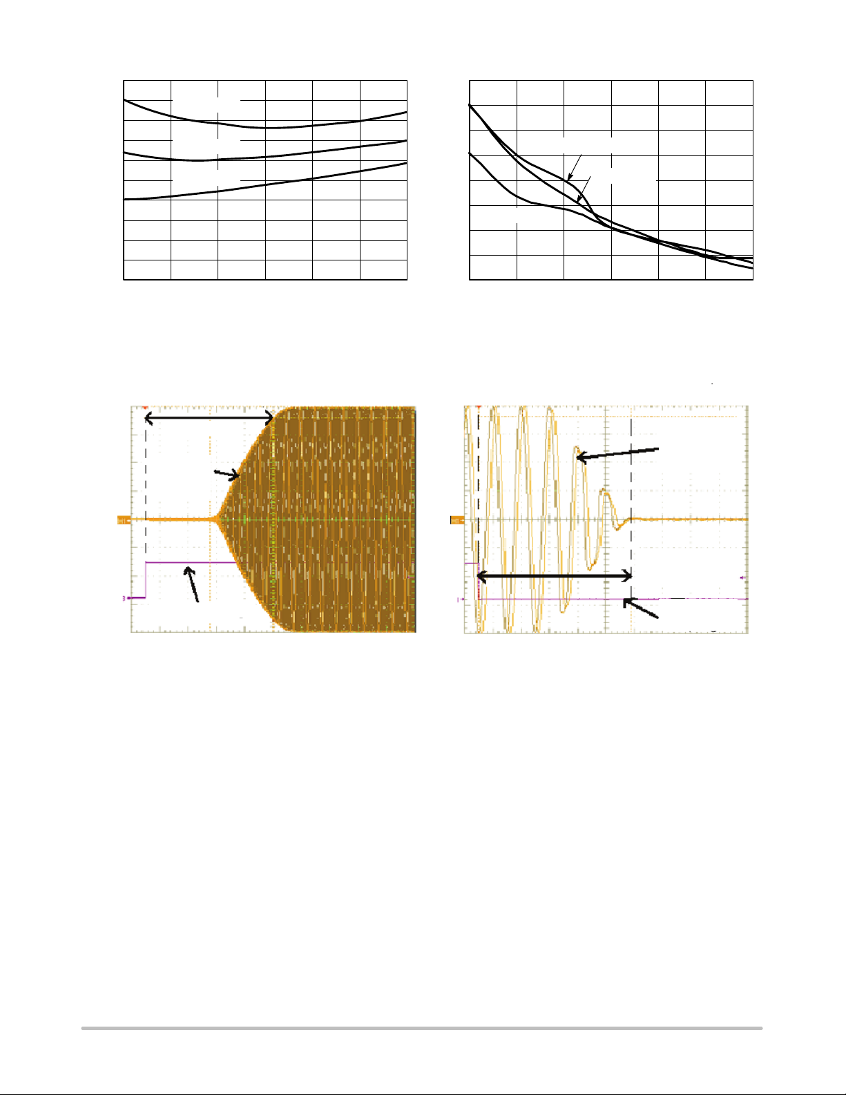
2.5 3.0 3.5 4.0
THD+N = 10%
POWER SUPPLY (V)
Figure 21. Output Power vs. Power Supply
= 8 @ f = 1 kHz
R
L
10
1.0
Vp = 2.5 V
THD+N (%)
0.1
Vp = 3.6 V
Vp = 5 V
THD+N = 1%
4.5 5.0
3.0
RL = 4
f = 1 kHz
THD+N = 10%
2.5 3.0 3.5 4.0
POWER SUPPLY (V)
(W)
out
P
2.5
2.0
1.5
1.0
0.5
0
Figure 22. Output Power vs. Power Suppy
RL = 4 @ f = 1 kHz
10
1.0
Vp = 2.5 V
THD+N (%)
0.1
Vp = 5 V
Vp = 3.6 V
THD+N = 1%
4.5
5.0
0.01
10
−20
−30
−40
−50
PSSR (dB)
−60
Vp = 3.6 V
−70
−80
10
Inputs Grounded, R
100 1000 10000 100000
FREQUENCY (Hz)
Figure 23. THD+N vs. Frequency
= 8 , P
R
L
Vp = 5 V
100 1000 10000 100000
= 250 mW @ f = 1 kHz
out
FREQUENCY (Hz)
Inputs to GND
RL = 8
Figure 25. PSRR vs. Frequency
= 8 , Vripple = 200 mvpkpk
L
0.01
10
100 1000 10000 100000
FREQUENCY (Hz)
Figure 24. THD+N vs. Frequency
−20
−30
−40
−50
PSSR (dB)
−60
−70
−80
10
= 4 , P
R
L
Vp = 3.6 V
Vp = 5 V
100 1000 10000 10000
= 250 mW @ f = 1 kHz
out
FREQUENCY (Hz)
Inputs to GND
Figure 26. PSRR vs. Frequency
Inputs grounded, RL = 4 , Vripple = 200 mVpkpk
RL = 4
http://onsemi.com
9

NCP9004
0
TYPICAL CHARACTERISTICS
−20
−30
−40
−50
CMMR (dB)
−60
−70
−80
10
100 1000 10000 100000
FREQUENCY (Hz)
Figure 27. PSRR vs. Frequency
= 3.6 V, RL = 8 , Vic = 200 mvpkpk
V
p
900
800
700
600
500
400
300
200
SHUTDOWN CURRENT (nA)
100
0
2.5
RL = 8
3.5 4.5 5.5
POWER SUPPLY (V)
Vp = 3.6 V
RL = 8
3.5
3.0
2.5
2.0
1.5
1.0
QUIESCENT CURRENT (mA)
0.5
0
120
130 140 150 160
TEMPERATURE (°C)
Thermal Shutdown
Vp = 3.6 V
RL = 8
Figure 28. Thermal Shutdown vs. Temperature
Vp = 5 V, RL = 8 ,
2.8
2.6
2.4
2.2
2.0
1.8
1.6
1.4
SHUTDOWN CURRENT (nA)
1.2
1.0
2.5
RL = 8
3.5 4.5 5.5
POWER SUPPLY (V)
Figure 29. Shutdown Current vs. Power Supply
= 8
R
L
1000
Vp = 3.6 V
RL = 8
NOISE (Vrms)
100
10
10
No Weighting
With A Weighting
100 1000 10000
FREQUENCY (Hz)
Figure 31. Noise Floor, Inputs AC Grounded
with 1 F Vp = 3.6 V
1000
100
NOISE (Vrms)
10
10
http://onsemi.com
10
Figure 30. Quiescent Current vs. Power Supply
= 8
R
L
Vp = 5 V
RL = 8
No Weighting
With A Weighting
100 1000 1000
FREQUENCY (Hz)
Figure 32. Noise Floor, Inputs AC Grounded
with 1 F Vp = 5 V
NCP9004
p
11
TA = +85°C
10
TA = +25°C
9
TA = −40°C
8
TURN ON TIME (mS)
7
6
2.5 3.5 4.5 5.5
POWER SUPPLY (V)
Figure 33. Turn on Time
Turn on time
Output
differential
voltage
8
7
TA = +25°C
6
TA = +85°C
5
TURN OFF TIME (mS)
4
2.5 3.5 4.5 5.5
TA = −40°C
POWER SUPPLY (V)
Figure 34. Turn off Time
Output
differential
voltage
Shutdown signal
024 20
6 8 10 12 14 16 18 0 1 2 10
(ms)
Figure 35. Turn on sequence
V
= 3.6 V, RL = 8
Turn off
time
Shutdown
signal
3456 789
(ms)
Figure 36. Turn off sequence
Vp = 3.6 V, RL = 8
http://onsemi.com
11

NCP9004
DESCRIPTION INFORMATION
Detailed Description
The basic structure of the NCP9004 is composed of one
analog pre−amplifier, a pulse width modulator and an
H−bridge CMOS power stage. The first stage is externally
configurable with gain−setting resistor Ri and the internal
fixed feedback resistor R
(the closed−loop gain is fixed by
f
the ratios of these resistors) and the other stage is fixed. The
load is driven differentially through two output stages.
The differential PWM output signal is a digital image of
the analog audio input signal. The human ear is a band pass
filter regarding acoustic waveforms, the typical values of
which are 20 Hz and 20 kHz. Thus, the user will hear only
the amplified audio input signal within the frequency range.
The switching frequency and its harmonics are fully filtered.
The inductive parasitic element of the loudspeaker helps to
guarantee a superior distortion value.
Power Amplifier
The output PMOS and NMOS transistors of the amplifier
have been designed to deliver the output power of the
specifications without clipping. The channel resistance
(Ron) of the NMOS and PMOS transistors is typically 0.3.
Turn On and Turn Off Transitions
In order to eliminate “pop and click” noises during
transition, the output power in the load must not be
established or cutoff suddenly. When a logic high is applied
to the shutdown pin, the internal biasing voltage rises
quickly and, 4 ms later, once the output DC level is around
the common mode voltage, the gain is established slowly
(5.0 ms). This method to turn on the device is optimized in
terms of rejection of “pop and click” noises. Thus, the total
turn on time to get full power to the load is 9 ms (typical)
(see Figure 35).
The device has the same behavior when it is turned−off by
a logic low on the shutdown pin. No power is delivered to the
load 5 ms after a falling edge on the shutdown pin
(see Figure 36). Due to the fast turn on and off times, the
shutdown signal can be used as a mute signal as well.
Shutdown Function
The device enters shutdown mode when the shutdown
signal is low. During the shutdown mode, the DC quiescent
current of the circuit does not exceed 1.5 A.
Current Breaker Circuit
The maximum output power of the circuit corresponds to
an average current in the load of 820 mA.
In order to limit the excessive power dissipation in the
load if a short−circuit occurs, a current breaker cell shuts
down the output stage. The current in the four output MOS
transistors are real−time controlled, and if one current
exceeds the threshold set to 1.5 A, the MOS transistor is
opened and the current is reduced to zero. As soon as the
short−circuit is removed, the circuit is able to deliver the
expected output power.
This patented structure protects the NCP9004. Since it
completely turns off the load, it minimizes the risk of the
chip overheating which could occur if a soft current limiting
circuit was used.
http://onsemi.com
12

NCP9004
APPLICATION INFORMATION
NCP9004 PWM Modulation Scheme
The NCP9004 uses a PWM modulation scheme with each
output switching from 0 to the supply voltage. If Vin = 0 V
outputs OUTM and OUTP are in phase and no current is
flowing through the differential load. When a positive signal
OUTP
OUTM
+Vp
0 V
−Vp
Load Current
0 A
Figure 37. Output Voltage and Current Waveforms into an Inductive Loudspeaker
DC Output Positive Voltage Configuration
is applied, OUTP duty cycle is greater than 50% and OUTM
is less than 50%. With this configuration, the current through
the load is 0 A most of the switching period and thus power
losses in the load are lowered.
Voltage Gain
The first stage is an analog amplifier. The second stage is
a comparator: the output of the first stage is compared with
a periodic ramp signal. The output comparator gives a pulse
width modulation signal (PWM). The third and last stage is
the direct conversion of the PWM signal with MOS
transistors H−bridge into a powerful output signal with low
impedance capability.
The total gain of the device is typically set to:
300 k
R
i
Input Capacitor Selection (Cin)
The input coupling capacitor blocks the DC voltage at the
amplifier input terminal. This capacitor creates a high−pass
filter with Rin, the cut−off frequency is given by
Fc +
2 Ri C
1
.
i
When using an input resistor set to 150 k, the gain
configuration is 2 V/V. In such a case, the input capacitor
selection can be from 10 nF to 1 F with cutoff frequency
values between 1 Hz and 100 Hz. The NCP9004 also
includes a built in low pass filtering function. It’s cut off
frequency is set to 20 kHz.
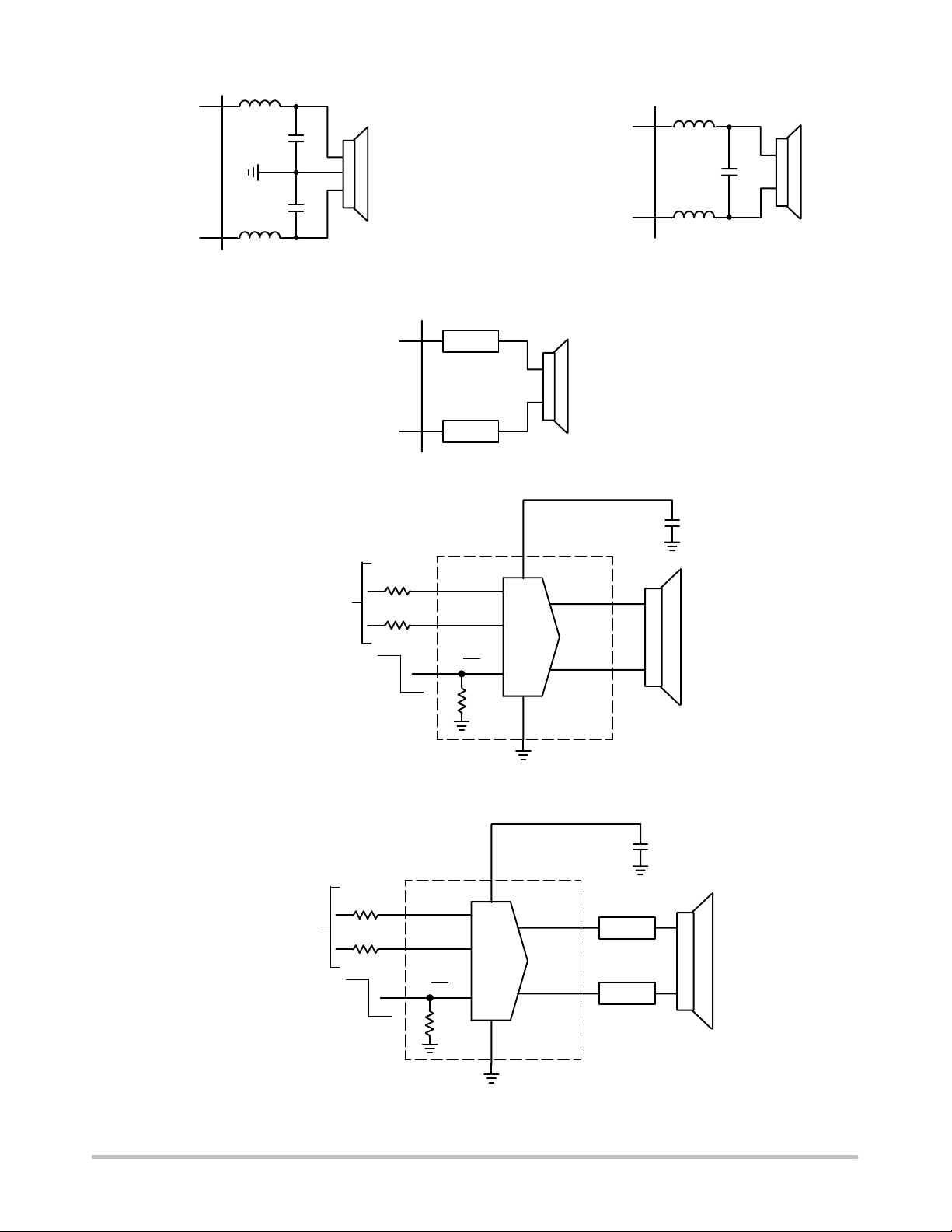
Optional Output Filter
This filter is optional due to the capability of the speaker
to filter by itself the high frequency signal. Nevertheless, the
high frequency is not audible and filtered by the human ear.
An optional filter can be used for filtering high frequency
signal before the speaker. In this case, the circuit consists of
two inductors (15 H) and two capacitors (2.2 F)
(Figure 38). The size of the inductors is linked to the output
power requested by the application. A simplified version of
this filter requires a 1 F capacitor in parallel with the load,
instead of two 2.2 F connected to ground (Figure 39).
Cellular phones and portable electronic devices are great
applications for Filterless Class−D as the track length
between the amplifier and the speaker is short, thus, there is
usually no need for an EMI filter. However, to lower radiated
emissions as much as possible when used in filterless mode,
a ferrite filter can often be used. Select a ferrite bead with the
high impedance around 100 MHz and a very low DCR value
in the audio frequency range is the best choice. The
MPZ1608S221A1 from TDK is a good choice. The package
size is 0603.
http://onsemi.com
13
NCP9004
OUTM
15 H
OUTM
15 H
2.2 F
8
=
L
R
OUTP
2.2 F
8
=
L
R
1.0 F
OUTP
15 H
15 H
Figure 38. Advanced Optional Audio Output Filter Figure 39. Optional Audio Output Filter
OUTM
FERRITE
CHIP BEADS
8
=
L
R
OUTP
Figure 40. Optional EMI Ferrite Bead Filter
Cs
Differential
Audio Input
from DAC
Input from
R
i
R
i
INP
INM
SD
VP
OUTM
OUTP
Microcontroller
GND
Figure 41. NCP9004 Application Schematic with Fully Differential Input Configuration
Cs
Differential
Audio Input
from DAC
Microcontroller
Input from
R
i
R
i
INP
INM
SD
VP
OUTM
FERRITE
CHIP BEADS
OUTP
GND
Figure 42. NCP9004 Application Schematic with Fully Differential Input Configuration and
Ferrite Chip Beads as an Output EMI Filter
http://onsemi.com
14

NCP9004
Cs
Differential
Audio Input
from DAC
C
i
C
i
Input from
Microcontroller
R
i
R
i
INP
INM
SD
VP
OUTM
FERRITE
CHIP BEADS
OUTP
GND
Figure 44. NCP9004 Application Schematic with Differential Input Configuration and
High Pass Filtering Function
Cs
Single−Ended Audio Input
from DAC
C
i
C
i
Input from
Microcontroller
R
i
R
i
INP
INM
SD
VP
OUTM
OUTP
Figure 43. NCP9004 Application Schematic with Single Ended Input Configuration
PCB Layout Information
NCP9004 is suitable for low cost solution. In a very small
package it gives all the advantages of a Class−D audio
amplifier. Due to its fully differential capability, the audio
signal can only be provided by an input resistor. If a low pass
filtering function is required, then an input coupling
capacitor is needed. The values of these components
determine the voltage gain and the bandwidth frequency.
The battery positive supply voltage requires a good
decoupling capacitor versus the expected distortion.
When the board is using Ground and Power planes with
at least 4 layers, a single 4.7 F filtering ceramic capactior
on the bottom face will give optimized performance.
GND
A 1.0 F low ESR ceramic capacitor can also be used with
slightly degraded performances on the THD+N from 0.06%
up to 0.2%.
In two layer application, if both Vp pins are connected on
the top layer, two decoupling capacitors will improve the
THD+N level. For example, a pair of capactors, 470 nF and
4.7 F, are good choices for filtering the power supply.
The NCP9004 power audio amplifier can operate from
2.5 V until 5.5 V power supply. With less than 2% THD+N,
it delivers 500 mW rms output power to a 8.0 load at
Vp =3.0 V and 1.0 W rms output power at V
= 4.0 V.
p
http://onsemi.com
15

NCP9004
Note
Figure 45. Top Layer
Note: This track between Vp pins is only needed when a 2 layers board is used. In case of a typical
4 or more layers, the use of laser vias in pad will optimize the THD+N floor.
ORDERING INFORMATION
Device Marking Package Shipping†
NCP9004FCT1G MAQ 9−Pin Flip−Chip CSP
(Pb−Free)
†For information on tape and reel specifications, including part orientation and tape sizes, please refer to our Tape and Reel Packaging
Specifications Brochure, BRD8011/D.
3000/Tape & Reel
http://onsemi.com
16

0.10 C
0.05
−C−
SEATING
PLANE
9 X b
0.05 C
0.03 C
4 X
0.10 C
C
A B
C
B
A
12 3
D
D1
NCP9004
PACKAGE DIMENSIONS
9−PIN FLIP−CHIP CSP
FC SUFFIX
CASE 499E
ISSUE O
−A−
−B−
E
A
A2
A1
e
E1
e
SOLDERING FOOTPRINT*
0.50
0.0197
NOTES:
1. DIMENSIONING AND TOLERANCING PER ANSI
Y14.5M, 1982.
2. CONTROLLING DIMENSION: MILLIMETERS.
3. COPLANARITY APPLIES TO SPHERICAL
CROWNS OF SOLDER BALLS.
MILLIMETERS
DIM MIN MAX
A 0.540 0.660
A1 0.210 0.270
A2
0.330 0.390
D 1.450 BSC
E
1.450 BSC
b 0.290 0.340
e 0.500 BSC
D1 1.000 BSC
E1 1.000 BSC
0.50
0.0197
0.265
0.01
SCALE 20:1
ǒ
inches
mm
Ǔ
*For additional information on our Pb−Free strategy and soldering
details, please download the ON Semiconductor Soldering and
Mounting Techniques Reference Manual, SOLDERRM/D.
ON Semiconductor and are registered trademarks of Semiconductor Components Industries, LLC (SCILLC). SCILLC reserves the right to make changes without further notice
to any products herein. SCILLC makes no warranty, representation or guarantee regarding the suitability of its products for any particular purpose, nor does SCILLC assume any liability
arising out of the application or use of any product or circuit, and specifically disclaims any and all liability, including without limitation special, consequential or incidental damages.
“Typical” parameters which may be provided in SCILLC data sheets and/or specifications can and do vary in different applications and actual performance may vary over time. All
operating parameters, including “Typicals” must be validated for each customer application by customer’s technical experts. SCILLC does not convey any license under its patent rights
nor the rights of others. SCILLC products are not designed, intended, or authorized for use as components in systems intended for surgical implant into the body, or other applications
intended to support or sustain life, or for any other application in which the failure of the SCILLC product could create a situation where personal injury or death may occur. Should
Buyer purchase or use SCILLC products for any such unintended or unauthorized application, Buyer shall indemnify and hold SCILLC and its officers, employees, subsidiaries, affiliates,
and distributors harmless against all claims, costs, damages, and expenses, and reasonable attorney fees arising out of, directly or indirectly, any claim of personal injury or death
associated with such unintended or unauthorized use, even if such claim alleges that SCILLC was negligent regarding the design or manufacture of the part. SCILLC is an Equal
Opportunity/Affirmative Action Employer. This literature is subject to all applicable copyright laws and is not for resale in any manner.
PUBLICATION ORDERING INFORMATION
LITERATURE FULFILLMENT:
Literature Distribution Center for ON Semiconductor
P.O. Box 5163, Denver, Colorado 80217 USA
Phone: 303−675−2175 or 800−344−3860 Toll Free USA/Canada
Fax: 303−675−2176 or 800−344−3867 Toll Free USA/Canada
Email: orderlit@onsemi.com
N. American Technical Support: 800−282−9855 Toll Free
USA/Canada
Europe, Middle East and Africa Technical Support:
Phone: 421 33 790 2910
Japan Customer Focus Center
Phone: 81−3−5773−3850
ON Semiconductor Website: www.onsemi.com
Order Literature: http://www.onsemi.com/orderlit
For additional information, please contact your local
Sales Representative
http://onsemi.com
17
NCP9004/D
 Loading...